INTRODUCTION
Keywords QCA cells, PLD design, VLSI technique, ALU technique, RLU 1.
Design and Development of 4-Bit Adder Programmable QCA Design using ALU Technique Aditya. N1 ,K.B. Ramesh2
Abstract QCA as the name suggests stands for Quantum dot Cellular Automata is a domain in nano technology employed in several digital circuits and stupendously used in electronics world. With the advancement in VLSI designs and technology, QCA design acts a powerful tool in modern day electronics in solving adder circuits. QCA cells can be utilized in many ways to study PLD design. This method basically proposes specialized architecture procedure to program devices and simulation is also done to tune QCA cells aimed for this specialized development design. This design provides an insight and idea about how adders are implemented in measuring and electronic instruments and their applications in the digital world. The performance of the respective QCA cell structures are simulated and it is tested by designer tools. It is cost effective and relatively uses very less equipment. This mainly discusses about the area and transistor count with propagation delay. The main idea of this paper is to show how QCA cells are implemented by ALU technique with 4 bit adder circuit.
International Research Journal of Engineering and Technology (IRJET) e ISSN: 2395 0056 Volume: 09 Issue: 02 | Feb 2022 www.irjet.net p ISSN: 2395 0072 © 2022, IRJET | Impact Factor value: 7.529 | ISO 9001:2008 Certified Journal | Page469
QCAisadomaininnanotechnologyusedinmodernsciencesandprovedinpresenteraanditissometimesinculcated andinstructedinCMOSsemiconductor[1]. Whiledesigningcircuits,theimportantelementisthatitisarriving atthe dimension which is a concern of possibility. It uses high power and leakage current. It is prominent and useful technology with minimum loopholes. A QCA cell is accounted of a couple of free electrons, probably confined in a potential [2]. It applies CMOS technology and operations of QCA are handled using ALU design. A polarized data is handled and four clocking systems are done periodically. There exists heavy work in every design of digital logic. An extensiveinnovative work inthefieldof a domainnamedfrilled technologymadeitfeasiblefor engineersand lessen the size of semiconductor. The uniqueness lies in finding an adder for 4 bit using carbon nanotubes and QCA cells based on the current CMOS based VLSI technology that can potentially increase scaling by lowering/hindering high powerconsumption. The mainadvantage ofhavingQCA cellsisthatit uses minimum power foraddercircuitsof 4 bits. ByusingMoore’s law we know that the total transistors gets an increase by 50% in CMOS rising to size reduction and high power dissipation[1].InALUdesigninQCAcellstheliteraturehaveimportantfeatureswhichincludesworkingundervarious temperaturesandtheamountofenergydissipatedfromthecircuit.Thisperfectlystrikesthechordandmomentumin the Thepaper.majorshortcomingslieswith theQCAcellswhichcontainsfourtoeightquantumspots,wherethepositionofthe electronsincolumbicisunidentifiedin1 bitALUcircuit.Thispaper depicts thatin advanced4 bitaddercircuitsthe design can be executed well by using ALU technique which performs logical as well as the arithmetic operations withoutanypropagationtimedelaywithease.
2. FUNDAMENTALS OF QCA CELLS:
2.1. QCA Cells:
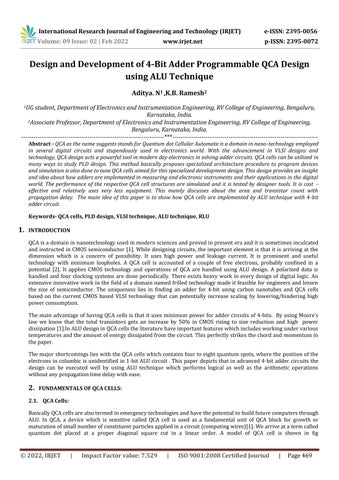
BasicallyQCAcellsarealsotermedinemergencytechnologiesandhavethepotentialtobuildfuturecomputersthrough ALU. In QCA, a device which is sensitive called QCA cell is used as a fundamental unit of QCA block for growth or maturationofsmallnumberofconstituentparticlesappliedinacircuit(computingwires)[1].Wearriveatatermcalled quantum dot placed at a proper diagonal square cut in a linear order. A model of QCA cell is shown in fig
1UG student, Department of Electronics and Instrumentation Engineering, RV College of Engineering, Bengaluru, Karnataka, India
2Associate Professor, Department of Electronics and Instrumentation Engineering, RV College of Engineering, Bengaluru, Karnataka, India. ***

© 2022, IRJET | Impact Factor value: 7.529 | ISO 9001:2008 Certified Journal | 470
1(a).Polarizationisaprocesswhereitisusedinfieldofelectromagneticradiationsinwhichthedirectionandmagnitude arespecifiedofavibratingparticle. Fig 1(a):amodelrepresentationofQCAcell.
Fig 1(b): processofQCA
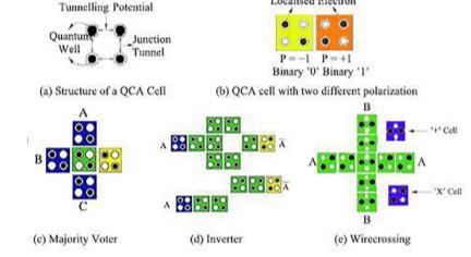
QCAclockingisadefinedastheareaswheretheconductionhappens,inotherwordsitcanbeexplainedastheyarethe conductive materials which modulate electron tunnelingbarriers of QCAcell in operation. The tunneling barrier hasa pair of Q dots in QCA cell where in the first stage cells where it stupendously increases. In the very first stage computation process takes place. In the second stage electrons of QCA cell are barred from entering the tunneling process.InthethirdstagethecellsofQCAmovesfromhigherthresholdtolowerthresholdlevels.Adetailedprocessis showninfig1(b).
International Research Journal of Engineering and Technology (IRJET) e ISSN: 2395 0056 Volume: 09 Issue: 02 | Feb 2022 www.irjet.net p ISSN: 2395 0072
TheimplementationofALUinCPUandfewotherapplicationshavecomplexdesignandcost effective[4]. Itisbasicallydividedintotwomodulesreverselogicunit(RLU)andreversiblearithmeticunit(RAU),ALUisflexibleis implementedinlogicgates
3. FUNCTIONALITIES OF ARITHMETIC LOGIC UNIT (ALU):
3.1. Reversible ALU:
Itisanarithmeticcircuitandanintegral component of CPUin the monitorsystem. The numberoflogical calculations selectedvariesdependingonthenumberofinputsandoutputsaccordingtothecircuit.ItiswidelyusedinQCAcellsto interpretoutputusingarithmeticlogic[2].
2.2. QCA clocking:
Page
International Research Journal of Engineering and Technology (IRJET) e ISSN: 2395 0056 Volume: 09 Issue: 02 | Feb 2022 www.irjet.net p ISSN: 2395 0072 © 2022, IRJET | Impact Factor value: 7.529 | ISO 9001:2008 Certified Journal | Page471
ThefunctionaldescriptionisshownbelowinFig2(b)andQCAcellsrepresentationin2(c).
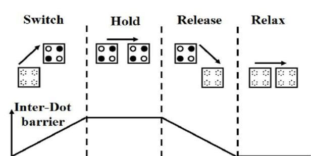
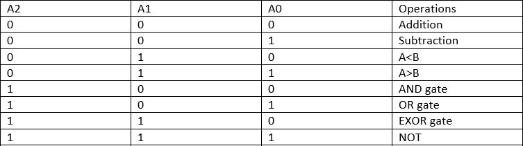
Fig 2(a): CircuitdiagramofReversibleALU 3.2. Reversible Logic Unit (RLU): Usually 4:1 Mux is generally preferred multiplexer and it is a 1 bit logic gates and acts a CNOT gate and uses 4RM gates connected in linear fashion. This can be then advanced to 4 bit adder gates also [2].The combinations of binary numbers such as 0 and 1 are tried in varied combinations in various gates and realized through A0,A1,A2,A3 by gates such as NOR,NAND,AND,ORandEX ORgates.
Fig 2(b): FunctionaldescriptionofRLU Fig 2(c): QCAdescriptionofRLU 3.3. Reverse Arithmetic Unit: A reverse arithmetic unit being a fundamental unit of ALU does the inverse operation of ALU .It consists of a full adder which has 5 input and 2 outputs. To this contrary there are 6 garbage outputs (G0, G1, G2, G3, G4, G5).These are the fundamentalfunctionalitiesofRAU[2].Ithasthefollowinginputs:M,N,O’,O’’,O’’’,O4.Itclocksnearly6clockdelays with atimedelay.Thefig2(d)showsafunctionaldescriptionofRAUandQCApictorialrepresentationin2(e).


International Research Journal of Engineering and Technology (IRJET) e ISSN: 2395 0056 Volume: 09 Issue: 02 | Feb 2022 www.irjet.net p ISSN: 2395 0072 © 2022, IRJET | Impact Factor value: 7.529 | ISO 9001:2008 Certified Journal | Page472
Fig 2(e): QCAdescriptionofRAU 3.4. Fault tolerance of RUG: This process occurs during QCA manufacturing which consists of various phases that include both deposition and synthesisphaseitincludesadditionalcellsandcellmisalignmentinreverseunitlogicdesign. WeuseVeriloglibraryfortheimplementationofQCAcells,thiscanbeconvertedintohardwarelanguagethatmajorly includesVerilogHDLdefinitionsandelementsofQCAlikefan out,fan in,andmanyotherapplicationsoflogicdesign. These QCA cells come from fault injection capability. It has a respective HDLQ Model of RUG. We assign certain variableslikeA,B,Y,whereP=1.Thefaulttoleranceisexplainedinfig2(f).
Fig 2(d):FunctionaldescriptionofRAUusingdecoders
Fig 2(f): FaulttoleranceofRUGbyQCAcells
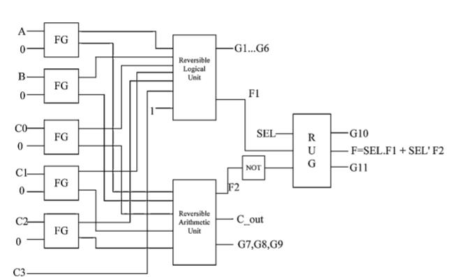


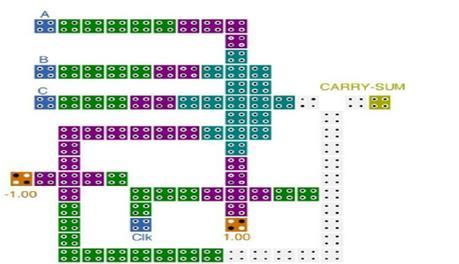
Fig 3(a): QCAcellsof1 bitadder Fig 3(b): Flowchartrepresentingadderprocess
4.1. Full Adder Circuits:
4. PROPOSED METHODOLOGIES:
Fig 2(g): ALUoperation
TheproposedoperationhasalogicaltouchperformedbyQCAcellswhichisexecutedbyaNOTgate.Thisdemonstrates thatXORgatehasaconfigurationratherthanconsideringthecellmethodprocess;theresultaccomplishestheimpactof QCAcellsoneachother.TheseXORgatesaremajorityinverterbased.Inputherearex,y,zwhiletheoutputcellis’a’.It has12QCAcellswherepolarization‘e’isaround‘+1’whichperformsXORfunction.
The basic functionalities of ALU processing unit consists of both arithmetic and logical expressions in ALU is of a full adder.ThisconsistsofaCo planarcrossoverwhichiswayadvancedcomparedtomultilayercrossoverthatQCAcellsare used 45 rotated functions are considered as not connected cells. These circuits have been designed according to the coplanarcrossover.Thesecircuitswitha1 bitadderasprimaryaddercircuitwhichincludesanotgatewhichactsasan inverterandthena majorityVoter.[1]ThisfulladderareA0,B0,CIareresultswheretheoutputisbothsumandcarry. And input is taken from 3 input Nand gate(IC 7410). This is performed by applying ALU technique through RLU (ReversibleLogicUnit).
Weuse selectlinesA2,A1,A0.Theproposedtableisshowninfig2(g).
QCAcellsplaysasignificantroleinRAU[4].QCAalsoreducespowerconsumptioninbothreversibleandnon reversible circuits in adiabatic and inherent environments. In most preferences, adiabatic circuits are irreversible where technologicalchangesaremadekeepingreversibilityandadiabaticprinciplesinmind.
© 2022, IRJET | Impact Factor value: 7.529 | ISO 9001:2008 Certified Journal | Page473
International Research Journal of Engineering and Technology (IRJET) e ISSN: 2395 0056 Volume: 09 Issue: 02 | Feb 2022 www.irjet.net p ISSN: 2395 0072
3.5. Design of a 4 Bit ALU design: Itisdesignedparticularlybasedonthelogicofcascadingafour1 bitALUbyintegratingall.Thisconsistsof: a) 4:1Multiplexer b) 2:1 Multiplexer to perform both arithmetic and logical operations. A single bit uses a complete full adder and one multiplexer.Thisisexplainedbyhavingonecompletefulladder andthreeMUX(Multiplexers).
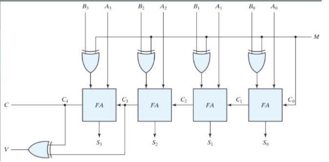
4.3. 4 bit adder implementation in QCA cells: In4 bitAdder,theproposedAdderisarrangedusingQCAandPLDdesignusingALUtechnique.Thiscanbeconsidered for the full adder output carry and linking a chain towards the input carry of the next adder. First to prepare a 4 bit binaryadderwehavetohavearipplecarrySiwhichisthesumofbitsAiandBi.TheinputCarryinisconnectedtothe nextadderandpropagatesconsequentlytotheendCout.Theproposeddesignisshownin3(c).
The designed 4 bit adder circuits which is dwelled by using QCA cells have arithmetic logic unit which does all the arithmetic operations like addition, multiplication, subtraction and division and the comparator operations too. The logicaloperationsproposedbyALUdoeslogicaloperationslikeAND,OR,NOTand,XOR.This4 bitadderiscomposedof fourALUunitsconnectedorcascadingfouronebitadder
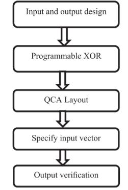
4.2. Flowchart: ThesefollowingflowchartsexplainsabouttheperformancemadebytheQCAtoolkit. Thisflowchartin3(b)represents 4 bit adder process and a vector input is given by a Lab View or Verilog Simulation Software [5]. Now coming to the simulationprocess,thisprocessendsandoutputresultistakenaccordingly.Theoutputcomesintheformofsinusoidal Twaveforms.heresultsaresumandcarryforanycircuit. Sum=A0’B0’C0+A0B0C0’+A0B0C0+A0B0’C0’ (2) Sum=A0(B0C0’+B0’C0)+A0’(B0’C0+B0C0’) (3) Sum=A0 ϴ B0 ϴC0 ϴ (4)where ϴ= Ex OR function Cout=(A0B0)+(B0C0)+(C0A0) (5) Equations(4)and(5)representsumandcarryofa 1 bitaddercircuit.Thisisupgradedto4 bitadder byusingsame logicusingQCAcellsandcascadingfour1 bitaddersforminga4 bitadder.
International Research Journal of Engineering and Technology (IRJET) e ISSN: 2395 0056 Volume: 09 Issue: 02 | Feb 2022 www.irjet.net p ISSN: 2395 0072
Fig 3(c): ProposeddesignofQCAcellsin4 bitadder
4.4. Logical and Arithmetic operations:
© 2022, IRJET | Impact Factor value: 7.529 | ISO 9001:2008 Certified Journal | Page474

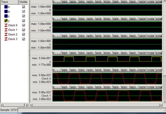
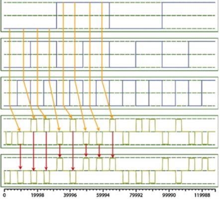
International Research Journal of Engineering and Technology (IRJET) e ISSN: 2395 0056 Volume: 09 Issue: 02 | Feb 2022 www.irjet.net p ISSN: 2395 0072 © 2022, IRJET | Impact Factor value: 7.529 | ISO 9001:2008 Certified Journal | Page475 Fig 3(d): Theschematicrepresentationof4 bitadders 5. RESULT/OUTPUT: A. 4 Bit Adder Simulation: Theseresultsthataretakenaftersimulationofthelayoutareshowninrespectivediagrams.Fig4(a)showstheexpected proposed4 bitQCAcellswhereasFig4(b)showstheexpectedinputandoutputwaveformsIofQCAcellssimulationsin simulationsoftwarelikeLabViewandVerilogsimulatedresults. Fig 4(a):expectedproposed4 bitQCAcells
International Research Journal of Engineering and Technology (IRJET) e ISSN: 2395 0056
©
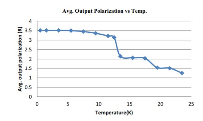
B. Polarization and temperature analysis: Whileanalyzingthesecircuitsof4 bitadderthepresenceofALUplaysaneffectivepart.WiththehelpofQCAcell itis importanttoknowaboutthisprocessasitisveryinterestingtoknowabouttheanalysisofQCAcells.Themainobjective is to find a reversible universal gate (RUG) [2]. If we increase the temperature, the average output polarization decreases.ThissimulationisdonepracticallyorbyothersoftwarelikeLabVieworQCAdesignertool.Fig4(c)showsthe temperaturev/saverageoutputgraphanalysis.Thecurveisnotlinearanddecreasesuponsomethreshold/breakdown region.
Certified Journal | Page476
Fig 4(b): expectedinputandoutputwaveformsdoneinLabViewSoftwareandQCADesignertool
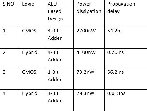
C. Comparison table of four bit adders: The output or result of power dissipation and propagation delay is calculated from 4 bit adders and respectively comparedwith1 bitadderALUcircuits withhavingtwotypesoflogic,i.e.:CMOSandhybridregionswiththegivenlogic .Therespectivecomparisonisshownintabularcolumninfig4(d).
Volume: 09 Issue: 02 | Feb 2022 www.irjet.net ISSN: 2395 0072 2022, IRJET | Impact Factor value: 7.529 | ISO 9001:2008
ItshowsrespectiveinputandoutputwaveformsoftheparticularQCAcells.ConsiderA,B,Casinputsandtheoutputis consideredas‘x’.Theexpectedproposed4 bitcellisbeingusedbyXORdesignwiththeQCAcells.Cinactsasanenable inputandCout,n0,n1,n2,n3actsasoutputsfor4 bitaddercircuits[3].These4 bitaddercircuitsarecalledasripple carryaddercircuit.Thisisacombinationofallfour1 bitaddercircuitsintegratedtogether.
p
Fig 4(c): Temperaturev/savg.outputpolarizationexpectedgraph
7. CONCLUSIONS:
Intheproposedworkwehaveearlierdiscussedaboutthedevelopmentof4 BitAddercircuitsusingQCAdesignbyALU technique which has provided a framework for advancement of 16 bit adders using VLSI technique. It had also confirmedtheacceptabilityofthecounterdesignofthecircuit.ThisjournalmainlyspeaksaboutvariousALUtechniques andhowtheyareusedtoforma4 bitaddercircuitbymanyprocesseswhichincludepolarization.Thecircuitswillhold theoperationstabilityonholdandmakestheQCAcellsinALUeffectiveandsustainablethusbeingusefultomajorityof peoplearoundtheworld.
International Research Journal of Engineering and Technology (IRJET) e ISSN: 2395 0056 Volume: 09 Issue: 02 | Feb 2022 www.irjet.net p ISSN: 2395 0072 © 2022, IRJET | Impact Factor value: 7.529 | ISO 9001:2008 Certified Journal | Page477 Fig 4(d): Comparisontableof4 bitALU
6. FUTURE SCOPE IN THIS AREA:
8. REFERENCES:
[1] G Mahindran, M. Periyaswamy, S.Murgeshwari, P.SWashburn, M.Susmitha”Design and execution of programmable logicdeviceusingquantumdotcellularautomata”,MaterialsToday:Proceedings,2021.
[3] M.Kapur, RezaSabaghi Nadooshan, K.Navi,” A novel design of 8 bit adder/subtractor by quantum dot cellular automata”,Journalofcomputerandsystemsciences.
VarioustechniquesofQCAdesignareemployedwhichincludes3bit,4bit,5bitbinarytograyconverterandgraytoBCD converter are presented using ALU technique. This is useful in storing precise data and information through codes. DesigningthelayoutcircuitsandsimulatingtheproposedlayoutisdoneusingQCADesignertool.Theproposeddesigns aredoneusingminimumnumberofcells,withminimumclockdelays.Someoftheresearchesshowsthatthedesignsare areaefficientandwithhighswitchingspeed/velocity.Theexpectedresultsareoncecheckedbyk mapsandverifiedby truth tables. QCA code converters logic circuits explains us detailing about the implementation. In near future these might help in minimizing error detection and leads to error free hardware units. ALU is basically used in all software applications and integration of QCA cells made integrate computer science domain with electronics domain in near futurewiththeadvancementinVLSItechniquenetworkaroundtheglobe.
[2]T.KSasamal,Ashutoshkumar,AnandMohana,”EfficientdesignofreversibleALUinquantum dotcellularautomata”, OptikAugust,25thApril2016.
ThegivenXORgatecarriedoutbyQCAcellsturnedouttobeasignificantlogicgateforcompositeQCAstructuredomain which further were fully utilized for complex configuration systems. The expected input and output waveforms were takenfromthedesignerkit.TheproposedmethodsusesverynewcomplexvaluesinLabView.Theproposedpowerand propagationdelayofCMOSandnormalALUarecalculatedinatabularcolumn.
Thus,inthispaperthemainobjectivesofreversibleALUwhichall togetherhadtwodomainsname,i.e.:RLUandRAU whichthoroughlyjustifiedbyprovidinganareaefficientmodelfor4bitaddercircuitsdesign.Thisreflectstheworkthat hasmoreprosoradvantagesinthefieldofVLSIinthenearfuturebecauseoflesspowerdissipationandefficientnoise removal.
[4] Surimala.P,Thomas,etal.,Studyonreversiblelogiccircuitsandanalysis,AICAAM,April2019.
[5] AhmedAbdul,“ImplementationofbinarytograycodeconvertersandgraytobinaryconvertersinQCAcells”,Nov2 2018.
International Research Journal of Engineering and Technology (IRJET) e ISSN: 2395 0056 Volume: 09 Issue: 02 | Feb 2022 www.irjet.net p ISSN: 2395 0072 © 2022, IRJET | Impact Factor value: 7.529 | ISO 9001:2008 Certified Journal | Page478