International Research Journal of Engineering and Technology (IRJET)
e-ISSN: 2395-0056
Volume: 09 Issue: 01 | Jan 2022
p-ISSN: 2395-0072
www.irjet.net
Simulating Ideal and Non-ideal Behavior of N-Channel MOSFET using Python Programming Shahabaj Mundaganur1, Aarbaj Mundaganur2 1Student,
Dept. of Electrical Engineering, University at Buffalo, New York, USA Dept. of Electrical Engineering, University at Buffalo, New York, USA ---------------------------------------------------------------------***---------------------------------------------------------------------2. PROPOSED METHODOLOGY Abstract - Metal Oxide Semiconductor Field Effect 2Student,
Transistor (MOSFET) is used in various analog and digital electronic devices. MOSFET devices can have ideal as well as non-ideal characteristics. Understanding these characteristics is essential to utilize the full potential of MOSFET devices. Open-source Python libraries like Tkinter, Matplotlib, and math are used. N-channel MOSFET is considered for these simulations. Different parameters like channel length modulation, body effect, and subthreshold conduction are considered for the non-ideal behavior of the NMOS device.
First, we will start with simulating the ideal behavior of the NMOS. NMOS ideally has three regions of operation- cut-off, linear, and saturation. Mathematical modeling for these three regions of operation of NMOS can be utilized to simulate the drain current and voltage characteristics of the NMOS using python. Table -1: Units and their symbol used for the design Symbol ID µn VGS VTH VDS VDS,sat
Key Words: Python, N-channel MOSFET, Body effect, Subthreshold conduction, Channel Modulation effect, ideal and non-ideal NMOS behavior
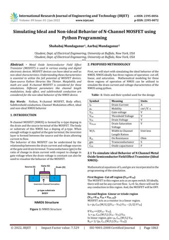
1. INTRODUCTION N-channel MOSFET (NMOS) is formed by n-type doping in the drain and the source terminal of the MOSFET. The body or substrate of this NMOS has a doping of p-type. When enough voltage is applied at the gate terminal, the inversion layer is formed between the source and the drain allowing current to flow. The behavior of this MOSFET can be understood by the relationship between the drain current and voltage sources at the gate and drain terminal. Transconductance (gm) is the ratio of change in drain current with respect to change in gate voltage when the drain voltage is constant can also be used to visualize the behavior of the MOSFET.
W/L Ron gm COX
Meaning Drain Current Mobility Gate voltage Threshold Voltage Drain Voltage Drain Saturation Voltage Width to Channel Length Ration On Resistance Transconductance Oxide capacitance
Units A cm2/V. s V V V V Unit less Ohm S F
2.1 To simulate ideal Behavior of N Channel Metal Oxide Semiconductor Field Effect Transistor (Ideal NMOS)Mathematical equations of ID and gm are incorporated in the programming of the simulation. First Region- Cut off region (VGS<VTH) The MOSFET in this region acts as an open switch. SO ideally, there will not be any current flow. ID=0. So, there will not be any conduction in this region. And, the MOSFET will be OFF. Second Region- Linear or triode region (VGS >VTH, VDS < VDS, sat)MOSFET acts as a resistor in a linear region. ID = n COX (W/L) [(VGS – VTH) VDS – (1/2) V2DS]
Figure 1: NMOS Structure
© 2022, IRJET
|
Impact Factor value: 7.529
If VDS <<2(VGS - VTH), ID = µn COX (W/L) (VGS - VTH) VDS In linear region, gm= µn Cox (W/L) VDS Ron= 1/ (µn Cox (W/L) (VGS - VTH))
|
ISO 9001:2008 Certified Journal
|
Page 1063