International Research Journal of Engineering and Technology (IRJET)
e-ISSN: 2395-0056
Volume: 08 Issue: 05 | May 2021
p-ISSN: 2395-0072
www.irjet.net
System Verilog/UVM Verification of AMBA APB Protocol Prameeth.H1, Aayushii Goswami2, Prajwal.M3, Vikas.N.G4, Dr. Rachana.S. Akki5 1 Student,
Department of Electronics and Instrumentation Engineering, RVCE, Bengaluru, India Department of Electronics and Instrumentation Engineering, RVCE, Bengaluru, India 3 Student, Department of Electronics and Instrumentation Engineering, RVCE, Bengaluru, India 4 Student, Department of Electronics and Instrumentation Engineering, RVCE, Bengaluru, India 5Assistant Professor, Department of Electronics and Instrumentation Engineering, RVCE, Bengaluru, India -------------------------------------------------------------------------***-----------------------------------------------------------------------2 Student,
Abstract
verification process usually takes up approximately 70% of the total time [3].
- The advancements in Very Large-Scale Integration (VLSI) technology have enabled packaging of billions of transistors on a single chip. Consequently, this has led to the increase in complexity of the System-on-Chip (SoC) design. One of the major components of SoC are the bus protocols which are the components that assist in communication on-chip or off-chip.
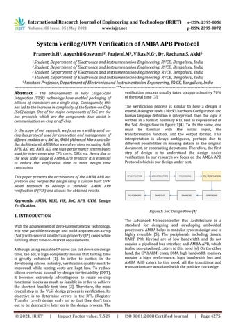
The verification process is similar to how a design is created. A designer reads a block's hardware Configuration and human language definition is interpreted, then the logic is written in a format, normally RTL text as represented in the SoC design flow in figure 1[4]. To do the same, one must be familiar with the initial input, the transformation function, and the output format. This interpretation is always ambiguous, perhaps due to different possibilities in missing details in the original document, or contrasting depictions. Therefore, the first step of design is to understand the design under verification. In our research we focus on the AMBA APB Protocol which is our design under test.
In the scope of our research, we focus on a widely used onchip bus protocol used for connection and management of different modules on a SoC i.e., AMBA (Advanced Microcontroller Bus Architecture). AMBA has several versions including AHB, APB, AXI etc. AHB, AXI are high performance system buses used for interconnecting CPU cores, DMA etc. Hence due to the wide scale usage of AMBA APB protocol it is essential to reduce the verification time to meet design time constraints. This paper presents the architecture of the AMBA APB bus protocol and verifies the design using a custom built UVM based testbench to develop a standard AMBA APB verification IP(VIP) and discuss the obtained results. Keywords: AMBA, VLSI, VIP, SoC, APB, UVM, Design Verification.
Figure1: SoC Design Flow [4]
1. INTRODUCTION
The Advanced Microcontroller Bus Architecture is a standard for designing and developing embedded processors. AMBA helps in modular system design and is highly reusable [5]. The peripherals including timers, UART, PIO, Keypad are of low bandwidth and do not require a pipelined bus interface and AMBA APB, which is also non-pipelined, caters to this need [6]. On the other hand, the CPU(ARM) cores, DMA, high bandwidth memory require a high performance, high bandwidth bus and AMBA AHB caters to this need. All the transitions and transactions are associated with the positive clock edge
With the advancement of deep-submicrometric technology, it is now possible to design and build a system-on-a-chip (SoC) with several intellectual-property (IP) cores while fulfilling short time-to-market requirements. Although using reusable IP cores can cut down on design time, the SoC's high complexity means that testing time is greatly enhanced [1]. In order to sustain in the developing silicon industry, verification quality must be improved while testing costs are kept low. To reduce silicon overhead caused by design-for-testability (DFT), it becomes extremely advantageous to reuse on-chip functional blocks as much as feasible in order to achieve the shortest feasible test time [2]. Therefore, the most crucial step in the VLSI design process is verification. Its objective is to determine errors in the RTL (Register Transfer Level) design early on so that they don't turn out to be destructive later on in the design process. The
© 2021, IRJET
|
Impact Factor value: 7.529
|
ISO 9001:2008 Certified Journal
|
Page 4275