International Research Journal of Engineering and Technology (IRJET)
e-ISSN: 2395-0056
Volume: 08 Issue: 05 | May 2021
p-ISSN: 2395-0072
www.irjet.net
Study of the MOSFET Parameters Effect on Drain and Transfer Characteristics Annesha Debnath1, Barnali Sikdar2, Pritha Kundu3, Purba Das4, Swati Barui5, Arnima Das6 1-4Student,
Department of Electronics and Communication Engineering, Narula Institute of Technology, West Bengal, India 5-6Assistant Professor, Department of Electronics and Communication Engineering, Narula Institute of Technology, West Bengal, India ---------------------------------------------------------------------***---------------------------------------------------------------------
Abstract - The goal of this paper is to observe the effect of
force for the positive gate voltage. The bound negative charges which are related with the acceptor atoms are present in the depletion region. A channel is formed when the electron reach there. [2]The electrons from the n+ source and drain regions are attracted into the channel formed by the positive voltages. Now, when we apply a voltage between the drain and source, the current flows amid the source and drain. If a negative voltage is given, a hole channel will be created below the oxide layer.
change of the MOSFET parameters on the value of its drain current. Designing the MOSFET with appropriate parameters like source area, drain area, and aspect ratio enables the design of integrated digital circuits with the best performance, depending on the selected MOSFET parameters and the operation conditions. Key Words: MOSFET structural parameters, drain characteristics, transfer characteristics, aspect ratio, drain current.
1. INTRODUCTION In digital electronic circuits the Metal Oxide Semiconductor Field Effect Transistor is considered as the essential element which is based on different types of MOS transistors. The MOSFET is the most widely used switching device in the design of digital integrated circuits based on the structure, the technological advantages, and the relative minimalism of MOSFET operation. [1] As compared to BJT, the MOSFET occupies a relativity smaller silicon area and has lower dissipation power. Because of these advantages it is possible to group many MOSFETs on a particular integrated circuit, resulting in the highest packing density of that digital integrated circuits. In this present study NMOS structure is considered for parametric variations like channel width, channel length, drain area, source area to signify the effect on transfer and drain characteristics. This in turn will enhance the MOSFET performance depending on different applications.[5]
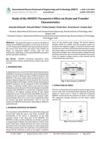
Fig -1: Block Diagram of MOSFET
3. STRUCTURE OF NMOS The four-terminal device having the terminals as gate, drain, source, body with a N-channel region between the heavily doped n+ source and n+ drain is called the N-channel MOSFET. In this device the substrate or body is of P-type. The negatively charged electrons are the major charge carriers. [4]
2. WORKING PRINCIPLE OF MOSFET The main theory of the MOSFET is to control the voltage and current flow amid the source and drain terminals. The functionality of the device is dependent on the MOS capacitor which is the main part of the MOSFET. The MOSFET acts like a switch. [3] By the use of either a positive or negative gate voltages, the semiconductor surface at the lower oxide layer, located between the source and drain terminal can be reversed from p-type to n-type respectively. The holes present under the oxide layer are pushed down along with the substrate as soon as we apply a repulsive © 2021, IRJET
|
Impact Factor value: 7.529
Fig -2: Structure of NMOS
|
ISO 9001:2008 Certified Journal
|
Page 4074