International Research Journal of Engineering and Technology (IRJET)
e-ISSN: 2395-0056
Volume: 07 Issue: 09 | Sep 2020
p-ISSN: 2395-0072
www.irjet.net
FULL ADDER DESIGN IMPLEMENTATION BY USING TRANSISTOR AND XNOR GATE Vinothkumar K1, Kavitha B2, Keerthana A3, Kowsalya Devi V4 1Professor,
Department of ECE, Muthayammal Engineering College, Tamilnadu, India Students, Departments of ECE, Muthayammal Engineering College, Tamilnadu, India ---------------------------------------------------------------------***---------------------------------------------------------------------2,3&4 UG
ABSTRACT In the technologically developing to reduce a time, space and increasing speed. This is 3 transistor xnor gate is proposed. The proposed XNOR gate is designed using Tanner tool and simulated using the Tanner S-edit technology. The proposed results are compared with the previous existing designs in terms of power and delay. It is also observed that the delay is reduced by 31.82% for three transistors XNOR gate and 28.76% for eight transistors full adder. Keywords: CMOS, full adder, exclusive-NOR (XNOR), low power, delay, transistors, VLSI, High-Level synthesis.
I. INTRODUCTION In present days, out of speed, area, time, power is the main issue in electronic design systems. Extra power consuming results in components overheating and makes the system failure so we need to design an IC’s which consumes less power became the main criterion in the various devices like mobile phones and laptops, High speed work stations etc. Day by day, power management has become the major issue and challenging task for improving battery life time and to reduce the charging time in the electronic handheld devices. The achievement fidelity applications. The characterization and raise of such low power multipliers will cooperation in comparison and choice of multiplier modules in system design. With drastic improvement of the electronic goods, lot of transformation is done and lot of technology is developed in the area of VLSI. More number of gates are integrating on the Chip changed the era of VLSI. So low power is the main area to be concentrated to reduce heat on chip and to extend the battery life and also chip life. The system specification is the processor.
II. METHODOLOGY This methodology for four bit ripple carry adder, eight transistors full adder and also discussed the low power analysis. This present four bit Ripple carry adder is mapped into Tanner tool and power and delay are decreased. The results is viewed using tanner s-edit tool. Basically it is also known as sequential adder and basic adder and it is also known as basic adder and sequential adder. The full adder comprises of two half adders and it can be realized using the gate delays. The Soc design consists of total power as static power and dynamic power. Dynamic power is the dissipated power when the device is in active mode. Static power is the power consumed when the device is in active mode but the signal values are unchanged.
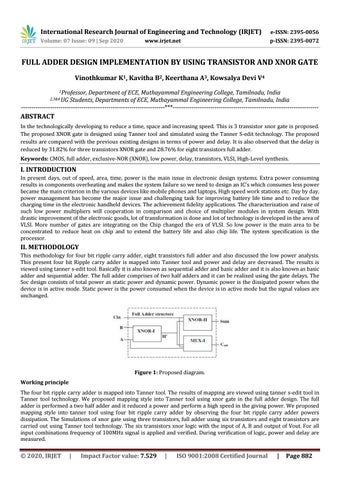
Figure 1: Proposed diagram. Working principle The four bit ripple carry adder is mapped into Tanner tool. The results of mapping are viewed using tanner s-edit tool in Tanner tool technology. We proposed mapping style into Tanner tool using xnor gate in the full adder design. The full adder is performed a two half adder and it reduced a power and perform a high speed in the giving power. We proposed mapping style into tanner tool using four bit ripple carry adder by observing the four bit ripple carry adder powers dissipation. The Simulations of xnor gate using three transistors, full adder using six transistors and eight transistors are carried out using Tanner tool technology. The six transistors xnor logic with the input of A, B and output of Vout. For all input combinations frequency of 100MHz signal is applied and verified. During verification of logic, power and delay are measured.
Š 2020, IRJET
|
Impact Factor value: 7.529
|
ISO 9001:2008 Certified Journal
|
Page 882