International Research Journal of Engineering and Technology (IRJET)
e-ISSN: 2395-0056
Volume: 07 Issue: 09 | Sep 2020
p-ISSN: 2395-0072
www.irjet.net
FINITE ELEMENT METHOD ANALYSIS OF ELECTRIC FIELD INDUCED PULL-IN DEVIATION IN NEM CONTACT SWITCHES B. Chanakya1, A. Arun ram2, E. Deva prasath3, S. Selvarasu4 1-3UG
Students, Department of ECE, Muthayammal Engineering College, Tamilnadu, India Department of ECE, Muthayammal Engineering College, Tamilnadu, India ---------------------------------------------------------------------***---------------------------------------------------------------------4Professor,
Abstract - The miniaturization trend leads to the
development of a graphene based Nano Electro Mechanical (NEM) switch to fulfill the high demand in low power device applications. In this article, we highlight the Finite Element Method (FEM) simulation of the graphene-based NEM switches of fixed-fixed ends design with beam structures which are perforated and intact. An external mechanical, electrical, or chemical stimulus can be detected and measured, and a response to the stimulus can be produced. Pull-in and pull-out characteristics are analyzed by using the FEM approach provided by COMSOL software. Key Words: Graphene, Pull-in deviation, Graphene analysis, Nano Electro Mechanical switch, COMSOL simulation, Finite Element Method simulation.
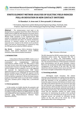
Fig -1: Structure of the beam The NCG deposited by PECVD contains both sp2- and sp3hybridized carbon atoms. The deposited NCG film is polycrystalline in nature. The polycrystalline nano graphene has randomly distributed grain orientation and size. The mechanical behavior of NCG depends on both the grain disorientations and the grain boundary rotation. Moreover, the mechanical strength of NCG depends on the arrangement of the defects in the NCG film. The NCG sheets have almost constant fracture stress and strain, and the fracture strength is independent of the grain size.
1. INTRODUCTION A Nano Electro Mechanical (NEM) switch is one of the promising devices to solve the problems of high power consumption in complementary metal-oxide semiconductor (CMOS) circuits. The NEM switch is built into logic circuits, relays, data storage, and high frequency communication because of its high ON-OFF current ratio and low leakage current. Graphene is one of the suggested 2D materials for high-performance NEM switch application because of its superior properties namely high electron mobility excess of 200,000 cm, superior current density capacity of 108 A/cm, the ultra-thin thickness of 0.335 nm and low resistivity of 1 W/cm. For these reasons, graphene-based NEM switch can provide better reliability and lower actuation pull-in voltage than a conventional switch.
1.2 Switching methods Self-aligned trench formation. The bottom electrode was intentionally over etched into the substrate, using the bottom electrode as a self-aligned etch mask. An SiO2 film deposited on the pre-patterned trench then formed the spacer structure, the thickness of which on the side edge of the bottom electrode was much less than that the top electrode was subsequently formed on the SiO2 spacer structure, which was later removed to create an air gap between the top and bottom electrodes (the profile of the air gap therefore being. We found that the depth of the trench and the deposition method are major tuning parameters for determining the profile of the sacrificial layer, which, in turn, determines the air gap structure. The proposed process can provide an extremely smooth surface on the side wall of the trench due to the planarization effect of the etching process.
1.1 Device geometry In this section, we briefly describe the geometry and operation principles of NEM switches. In our earlier work, we experimentally studied the switching operation of Nano Crystalline Grapheme (NCG) beam NEM switches. The NCG was synthesized by direct deposition of NCG on a Si/SiO2 substrate using Plasma-Enhanced Chemical Vapor Deposition (PECVD).
© 2020, IRJET
|
Impact Factor value: 7.529
|
ISO 9001:2008 Certified Journal
|
Page 778