International Research Journal of Engineering and Technology (IRJET) Volume: 07 Issue: 08 | Aug 2020
e-ISSN: 2395-0056 p-ISSN: 2395-0072
www.irjet.net
HIGH-SPEED LOW-POWER WIRELESS FREQUENCY TO VOLTAGE CONVERTER USING CMOS CONVERTER Prabhakar Babu1, Gyanendra Kumar Verma2, Ajeet Kumar3 1,3PG
scholar, Department of Electronics and Communication Engineering, Axis Institute of Technology and management Kanpur 2Assistant Professor, Department of Electronics and Communication Engineering, 3Naraina Vidyapeeth Engineering and Management Institute Panki, Kanpur -------------------------------------------------------------------------***---------------------------------------------------------------------Abstract - For this work, a high-speed low-power (LHF) wireless converter (FVC) based on two models was developed and implemented. The Multisim program is used to construct the first version. This consists of two RMS-DC converters, a differentiator and a splitter. The proposed converter includes a specific output and a linear transition function without ripples. The second version is designed with the help of the Tanner EDA system. The differentiator consists of two voltages for the new transformer, two RMSDC converters and a separator. The proposed converter provides a stable output and linear propagation mechanism without ripples and is suitable for high-frequency applications. The downside of the second edition of the first edition is that it can be extended to the GHz frequency range as it is optimized with existing CMOS circuits..
( )
( ) Where
(
) (2)
is the time constant of the differentiator.
After applying converters, we get √
( ) and
( ) into
the
RMS-DC
(3) (4)
√
Thus dividing
in (4) by
in (3), we get
(5) Where,
Key words: - Frequency to Voltage Converter (FVC), CMOS, RMS-DC, MOSFET, analogue to digital converters (ADCs), digital to analogue converters (DACs), variable gain amplifiers (VGAs).
And,
is the sensitivity of the converter is the scaling factor (gain) of the divider
It is clearly seen from equation (5) that the output signal is linearly proportional to the input frequency, , and insensitive to the input signal amplitude, .
1.1 Introduction In this segment, we have introduced and implemented Frequency to Voltage Converter (FVC) using current CMOS circuits. The simulation of the planned circuit was conducted using the Tanner EDA 180 nm technology with a different supply voltage. Both circuits were tested with the same input condition for a good synthesis of comparative analysis. Within this portion, we have also measured the power consumption of all circuits at various power supply voltages [3, 5].
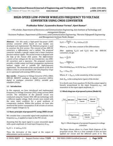
1.3 Block diagram of proposed system (Model-II)
1.2 Basic principle of proposed FVC using CMOS circuit We consider that a sinusoidal signal with amplitude frequency is applied as input in the FVC circuit.
and
Assuming that the input signal is a pure sinusoidal signal with a peak amplitude of and input frequency of ( )
(
Fig.1.1: Block diagram of proposed frequency to voltage converter
) (1)
The figure shown above is a basic block diagram of the proposed circuit. This is a clear example of how we have applied our circuit and the different parts of it. This
Then, the derivative of this signal at the output of differentiator can be written as
© 2020, IRJET
|
Impact Factor value: 7.529
|
ISO 9001:2008 Certified Journal
|
Page 3478