International Research Journal of Engineering and Technology (IRJET)
e-ISSN: 2395-0056
Volume: 07 Issue: 03 | Mar 2020
p-ISSN: 2395-0072
www.irjet.net
REALIZATION OF POWER OPTIMISED CARRY SKIP ADDER USING AOI LOGIC ALMUKHTAR AHMED1, NASER ALINABE2 1Faculty
of Engineering, Sabratha University, SABRATHA, LIBYA, ASSIST.PROF,DEPT.OF ELE &ELEC ENG,FACULTY OF ENG,SABRATHA-LIBYA 2faculty of Education, ZINTAN UNIVERSITY, ZITAN, LIBYA, LECTURER, DEP OF MATH. FACULTY OF EDUCATION, ZINTAN-LIBYA ------------------------------------------------------------------------***-----------------------------------------------------------------------
Abstract:- The binary adder is the critical element in most digital circuit designs. The more important parameters in VLSI design are power consumption, area and speed. And since the binary adder is exist in most digital circuit designs. In this paper a carry skip adder (CSKA)based AND-OR INVERTER (AOI)logic is proposed in order to reduce area and power consumption. The proposed adder is simulated by Xilinx and compared with the conventional CSKA based multiplexer logic
voltage level through the drain-induced barrier lowering effect. Depending on the amount of the supply voltage reduction, the operation of ON devices may reside in the super threshold, near-threshold, or sub threshold regions. Working in the super threshold region provides us with lower delay and higher switching and leakage powers compared with the near/sub threshold regions.
Key words-Carry skip adder (CSKA), AND-OR-INVERTER, Xilinx Simulation.
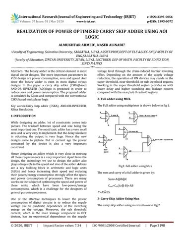
The Full adder using multiplexer is shown below in fig 1.
2- Full adder using MUX.
1-INTRODUCTION While designing an adder, lot of constraints comes into picture. The tradeoff between speed and size being the most important one. The most basic adder has a very small area and is very easy to implement. But the delay involved in obtaining the output is very huge. Hence the new designs came to picture. But in current age the power consumed by the device is also a very important constraint. Hence designing an adder which is very close in meeting all these requirements is a very important. Apart from the design, the technology we use to design the adder also plays a huge role in the speed and size of the adder. Adders are a key building block in arithmetic and logic units (ALUs) and hence increasing their speed and reducing their power/energy consumption strongly affect the speed and power consumption of processors. There are many works on the subject of optimizing the speed and power of these units, which have been low-power/energy consumptions, which is a challenge for the designers of general purpose processors. One of the effective techniques to lower the power consumption of digital circuits is to reduce the supply voltage due to quadratic dependence of the switching energy on the voltage. Moreover, the sub threshold current, which is the main leakage component in OFF devices, has an exponential dependence on the supply
© 2020, IRJET
|
Impact Factor value: 7.34
|
Fig1: full adder using Mux The sum and carry of a full adder is given by: Sum=A⊕B⊕C Cout=Cin(A ⊕ B)+AB Y=AS+BS 3- Carry Skip Adder Using Mux The carry skip adder using mux is shown in Fig 2 .
ISO 9001:2008 Certified Journal
|
Page 3198