International Research Journal of Engineering and Technology (IRJET)
e-ISSN: 2395-0056
Volume: 07 Issue: 03 | Mar 2020
p-ISSN: 2395-0072
www.irjet.net
Design of 1 Bit ALU using Various Full Adder Circuits V. Hari babu1, K. Saitejasri2, D. Alekya3, D. Naveen Yadav4 1V.
Hari babu: Assistant Professor, Dept. of Electronics and Communication Engineering, Malla Reddy Institute of Technology and Science, Telangana, India. 2K. Saitejasri: Dept. of Electronics and Communication Engineering, Malla Reddy Institute of Technology and Science, Telangana, India. 3D. Alekya: Dept. of Electronics and Communication Engineering, Malla Reddy Institute of Technology and Science, Telangana, India. 4D. Naveen Yadav: Dept. of Electronics and Communication Engineering, Malla Reddy Institute of Technology and Science, Telangana, India. ---------------------------------------------------------------------***---------------------------------------------------------------------
Abstract - This paper explores design of 1-bit ALU using
various full adder techniques such as Transmission Gate(TG), Complementary Metal Oxide Semiconductor(CMOS), Gate Diffusion Input(GDI), Modified GDI logic. The main design objective is to implement 1-bit ALU using different full adders providing low powered and high speed with voltage swing. GDI is one of the area effective, high speed and low power technique. It needs smallest amount of transistors compared to CMOS technology. 1-bit ALU is designed in 180nm, 130nm technologies.
III represents implementation of various full adder technologies. Section IV represents design of 1bit ALU using full adder techniques. Section V represents their performance comparison.
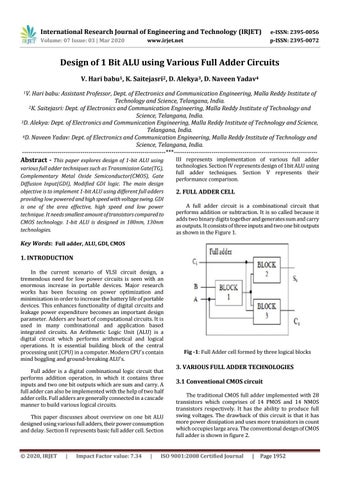
2. FULL ADDER CELL A full adder circuit is a combinational circuit that performs addition or subtraction. It is so called because it adds two binary digits together and generates sum and carry as outputs. It consists of three inputs and two one bit outputs as shown in the Figure 1.
Key Words: Full adder, ALU, GDI, CMOS 1. INTRODUCTION In the current scenario of VLSI circuit design, a tremendous need for low power circuits is seen with an enormous increase in portable devices. Major research works has been focusing on power optimization and minimization in order to increase the battery life of portable devices. This enhances functionality of digital circuits and leakage power expenditure becomes an important design parameter. Adders are heart of computational circuits. It is used in many combinational and application based integrated circuits. An Arithmetic Logic Unit (ALU) is a digital circuit which performs arithmetical and logical operations. It is essential building block of the central processing unit (CPU) in a computer. Modern CPU's contain mind boggling and ground-breaking ALU's. Full adder is a digital combinational logic circuit that performs addition operation, in which it contains three inputs and two one bit outputs which are sum and carry. A full adder can also be implemented with the help of two half adder cells. Full adders are generally connected in a cascade manner to build various logical circuits. This paper discusses about overview on one bit ALU designed using various full adders, their power consumption and delay. Section II represents basic full adder cell. Section
Š 2020, IRJET
|
Impact Factor value: 7.34
|
Fig -1: Full Adder cell formed by three logical blocks
3. VARIOUS FULL ADDER TECHNOLOGIES 3.1 Conventional CMOS circuit The traditional CMOS full adder implemented with 28 transistors which comprises of 14 PMOS and 14 NMOS transistors respectively. It has the ability to produce full swing voltages. The drawback of this circuit is that it has more power dissipation and uses more transistors in count which occupies large area. The conventional design of CMOS full adder is shown in figure 2.
ISO 9001:2008 Certified Journal
|
Page 1952