International Research Journal of Engineering and Technology (IRJET)
e-ISSN: 2395-0056
Volume: 06 Issue: 07 | July 2019
p-ISSN: 2395-0072
www.irjet.net
DESIGN AND IMPLEMENTATION OF HIGH SPEED, LOW POWER CHARGE SHARED RESET METHOD BASED DYNAMIC LATCH COMPARATOR USING 45nm CMOS TECHNOLOGY SHUBHASHREE P R1, SAVIDHAN SHETTY C S2 1Student,
Dept. of ECE, Sahyadri College of Engineering & Management, Karnataka, India Professor, Dept. of ECE, Sahyadri College of Engineering & Management, Karnataka, India ---------------------------------------------------------------------***---------------------------------------------------------------------2Assistant
Abstract - An analog to digital converter (ADC) is an
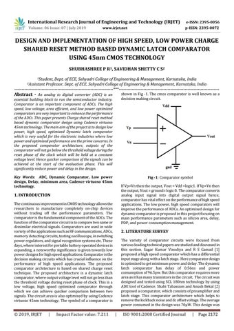
shown in Fig -1. The cmos comparator is well known as a decision making circuit.
essential building block to run the semiconductor industry. Comparator is an important component of ADCs. The high speed, low voltage, area efficient, and low power optimized comparators are very important to enhance the performance of the ADCs. This paper presents Charge shared reset method based dynamic comparator design using Cadence virtuoso 45nm technology. The main aim of the project is to design low power, high speed, optimized Dynamic latch comparator which is very useful for the electronic industries where low power and optimized performance are the prime concerns. In the proposed comparator architecture, outputs of the comparator will not go below the threshold voltage during the reset phase of the clock which will be held at a constant voltage level. Hence quicker comparison of the signals can be achieved at the start of the evaluation phase. This will significantly reduce power and delay in the design. Key Words: ADC, Dynamic Comparator, Low power design, Delay, minimum area, Cadence virtuoso 45nm technology.
Fig -1: Comparator symbol If Vp>Vn then the output, Vout = Vdd =logic1. If Vp<Vn then the output, Vout = ground= logic 0. The comparator converts analog input signal into digital output signal hence, comparator has vital effect on the performance of high speed applications. The low power, high speed comparators will improve the performance of ADCs. An optimized design for dynamic comparator is proposed in this project focusing on main performance parameters such as silicon area, delay, PDP, and power consumption management.
1. INTRODUCTION The continuous improvement in CMOS technology allows the researchers to manufacture completely on-chip devices without trading off the performance parameters. The comparator is the fundamental component of the ADCs. The function of the comparator circuit is to compare two same or dissimilar electrical signals. Comparators are used in wide variety of the applications such as RF communications, ADCs, memory detecting circuits, testing oscilloscope, in switching power regulators, and signal recognition systems etc. These days, where interest for portable battery operated devices is expanding, a noteworthy significance is given towards low power designs for high speed applications. Comparator is the decision making circuits which has crucial influence on the performance of high speed applications. The proposed comparator architecture is based on shared charge reset technique. The proposed architecture is a dynamic latch comparator, where output voltage level will not go less than the threshold voltage during reset phase of clock. This is a low voltage, high speed optimized comparator through which we can achieve quicker comparison between two signals. The circuit area is also optimized by using Cadence virtuoso 45nm technology. The symbol of a comparator is
Š 2019, IRJET
|
Impact Factor value: 7.211
2. LITERATURE SURVEY The variety of comparator circuits were focused from various leading technical papers are studied and discussed in this section. Sagar Kumar Vinodiya and R S Gamad [1] proposed a high speed comparator which has a differential input stage along with a latch stage. Here comparator design is optimized to get minimum power and delay. The dynamic latch comparator has delay of 0.56ns and power consumption of 96.5pw. But this comparator requires more area as it has many transistors in the circuit. The circuit was designed and tested using SCL 180nm technology by using ADE tool of Cadence. Shabi Tabassum and Anush Bekal [2] proposed a comparator, which consists of preamplifier and latch stage. This comparator architecture which helps to remove the kickback noise and dc offset voltage. The average power consumed in the design was 70ÂľW. This design was
|
ISO 9001:2008 Certified Journal
|
Page 2172