International Research Journal of Engineering and Technology (IRJET)
e-ISSN: 2395-0056
Volume: 06 Issue: 1 | Dec 2019
p-ISSN: 2395-0072
www.irjet.net
32nm FinFET Based Comparator for Flash ADC Lijesh L1, Supriya Sara Mathew2 1Associate
Professor, Deapartment of ECE, Musaliar College of Engineering and Technology, Kerala, India Scholar, Deapartment of ECE, Musaliar College of Engineering and Technology, Kerala, India ---------------------------------------------------------------------***---------------------------------------------------------------------2PG
Abstract - Power consumption is a major problem in all
is conceivable. Comparator design is also a challenge for design of Flash ADCs.
electronic circuits. In order to achieve the power consumption, circuit scaling is important. In CMOS based circuits scaling should be possible up to constrained range after that it will present short channel impacts. To defeat above disadvantage FINFET has been presented. Comparator is one of the components most importantly required in analog to digital converter. Op-Amps are the major constituent of analog and mixed-signal systems. Speed interest for rapid applications, for example, ADC and DAC lead to expanded interest for amplifiers with high gain and speed. FinFET is a standout amongst the most encouraging advancements to structure underneath 50nm. FinFET transistors in simple circuit configuration presents noteworthy enhancement contrasted with conventional one entryway CMOS structure. In this paper, we present a FINFET based comparators for high speed Flash ADC. The main parameters considered in the performance analysis are delay, frequency and power consumption. LTSpice simulation software is used for design and analysis of the comparator circuits in the above specified 32nm scaling range.
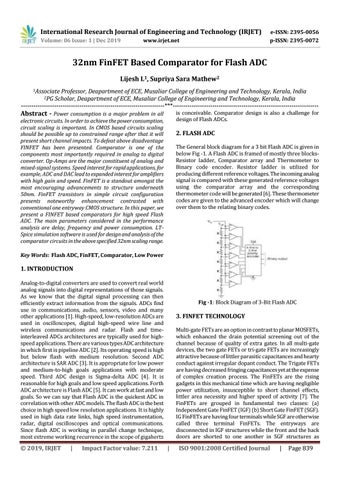
2. FLASH ADC The General block diagram for a 3 bit Flash ADC is given in below Fig -1. A Flash ADC is framed of mostly three blocksResistor ladder, Comparator array and Thermometer to Binary code encoder. Resistor ladder is utilized for producing different reference voltages. The incoming analog signal is compared with these generated reference voltages using the comparator array and the corresponding thermometer code will be generated [6]. These thermometer codes are given to the advanced encoder which will change over them to the relating binary codes.
Key Words: Flash ADC, FinFET, Comparator, Low Power
1. INTRODUCTION Analog-to-digital converters are used to convert real world analog signals into digital representations of those signals. As we know that the digital signal processing can then efficiently extract information from the signals. ADCs find use in communications, audio, sensors, video and many other applications [1]. High-speed, low-resolution ADCs are used in oscilloscopes, digital high-speed wire line and wireless communications and radar. Flash and timeinterleaved ADCs architectures are typically used for highspeed applications. There are various types ADC architecture in which first is pipeline ADC [2]. Its operating speed is high but below flash with medium resolution. Second ADC architecture is SAR ADC [3]. It is appropriate for low power and medium-to-high goals applications with moderate speed. Third ADC design is Sigma-delta ADC [4]. It is reasonable for high goals and low speed applications. Forth ADC architecture is Flash ADC [5]. It can work at fast and low goals. So we can say that Flash ADC is the quickest ADC in correlation with other ADC models. The flash ADC is the best choice in high speed low resolution applications. It is highly used in high data rate links, high speed instrumentation, radar, digital oscilloscopes and optical communications. Since flash ADC is working in parallel change technique, most extreme working recurrence in the scope of gigahertz
Š 2019, IRJET
|
Impact Factor value: 7.211
Fig -1: Block Diagram of 3-Bit Flash ADC
3. FINFET TECHNOLOGY Multi-gate FETs are an option in contrast to planar MOSFETs, which enhanced the drain potential screening out of the channel because of quality of extra gates. In all multi-gate devices, the two gate FETs or tri-gate FETs are increasingly attractive because of littler parasitic capacitances and hearty conduct against irregular dopant conduct. The Trigate FETs are having decreased fringing capacitances yet at the expense of complex creation process. The FinFETs are the rising gadgets in this mechanical time which are having negligible power utilization, insusceptible to short channel effects, littler area necessity and higher speed of activity [7]. The FinFETs are grouped in fundamental two classes: (a) Independent Gate FinFET (IGF) (b) Short Gate FinFET (SGF). IG FinFETs are having four terminals while SGF are otherwise called three terminal FinFETs. The entryways are disconnected in IGF structures while the front and the back doors are shorted to one another in SGF structures as
|
ISO 9001:2008 Certified Journal
|
Page 839