International Research Journal of Engineering and Technology (IRJET)
e-ISSN: 2395-0056
Volume: 05 Issue: 09 | Sep 2018
p-ISSN: 2395-0072
www.irjet.net
Analysis of BJT with respect to JFET Biasing Md Zubair Khan1, Syed Mustafa2, Noor Ul Abedin3, Dr. Syeda Gauhar Fatima4 1,2Undergraduate
B.E (E.C.E) Student, Deccan College of Engineering and Technology - Hyderabad Postgraduate M.E (E.C.E – D.S.E) Student, University College of Engineering (A), O.U - Hyderabad 4 Professor, Dept of E.C.E, Deccan College of Engineering and Technology - Hyderabad ---------------------------------------------------------------------***--------------------------------------------------------------------3
Abstract – As transistor is the major element for amplification. Well aware the common two types of transistor are BJT and JFET, used in analog electronics extending upto working as a switch in digital electronics. In this work the obtained output voltage of JFET when biased is analyzed, keeping in same analyzing a BJT with the same operating conditions. Giving significance to appropriate portions of BJT and JFET respectively.
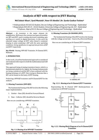
1.2 Biasing Transistor (N-CHANNEL JFET) The fundamental biasing of the JFET involves the biasing with the voltage across Gate – Source (VGS) Reversed Biased. Here we are considering an N-Channel JFET transistor.
Key Words: Biasing, NPN BJT Transistor, N-Channel JFET, Multisim. 1. INTRODUCTION In this work, a lucid but fundamental approach is considered and analysed with respect to both the mathematical and CAD approach. This approach being of analog transistors basics, which is a fundamental platform for digital, the biasing fundamentals are being considered and the BJT is been analysed with the biasing technique of a JFET. Here trying to illustrate that a BJT can be biased on the basis of JFET biasing. Preferring a NPN BJT transistor and N-Channel JFET for the analysis. Fig -1.2.1 : Biasing of an N-Channel JFET Transistor
1.1 Biasing Transistor (NPN BJT) The fundamental biasing of the BJT involves the following major implementation: 1.
Emitter – Base (EB) should be Forward Biased.
2.
Base – Collector (BC) should be Reverse Biased.
Representing the N Channel JFET blocks/portions on comparison to NPN BJT transistor.
Here we are considering a NPN BJT transistor.
Fig -1.2.2 : Biasing Block Diagram of an N-Channel JFET Transistor
Fig -1.1: Biasing of an NPN BJT Transistor © 2018, IRJET
|
Impact Factor value: 7.211
|
ISO 9001:2008 Certified Journal
|
Page 251