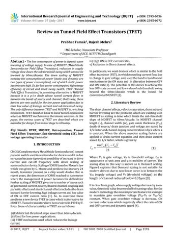
International Research Journal of Engineering and Technology (IRJET)
e-ISSN: 2395-0056
Volume: 04 Issue: 07 | July -2017
p-ISSN: 2395-0072
www.irjet.net
Review on Tunnel Field Effect Transistors (TFET) Prabhat Tamak1, Rajesh Mehra2 1ME
Scholar, 2Associate Professor of ECE, NITTTR Chandigarh ---------------------------------------------------------------------***--------------------------------------------------------------------1,2Department
Abstract - The low consumption of power is depends upon
lowering of voltage supply. In case of MOSFET (Metal Oxide Semiconductor Field Effect Transistor), reduction in supply voltage slow down the sub threshold swing which cannot be lowered by 60mv/decade. The down scaling of MOSFET increase the consumption of power (static and dynamic are two types of power consumption), out of which static power becomes too high. So, for low power consumption, high energy efficiency of circuit and small swing switch, TFET (Tunnel Field Effect Transistors) is promising alternative to MOSFET because it is a p-i-n diode whose tunnel current flows in between the bands of source and channel, that’s why, these devices are very useful for the low power application due to their low value of leakage current and sub threshold swing. The only difference between TFET and MOSFET is switching mechanism, TFET based on band to band tunnel mechanism where as MOSFET mechanism is thermionic emission. In this paper, the various types of TFET are described which are available for design from initial stage to till today.
Key Words: BTBT, MOSFET, Hetro-junction, Tunnel Field Effect Transistor, Sub threshold swing (SS), low voltage operating transistor.
1. INTRODUCTION
iv) High ON to OFF current ratio. v) Reduction in Short channel effects. In particulars, we want devices which is similar to the field effect transistor (FET), in which tunneling current flow due to change in gate voltage, and, used the band to band tunnel mechanism in the ON state and in alteration between OFF and ON state[1]. The potential of this device to achieve the less OFF state current and low value of sub threshold swing beyond the 60mv/decade which is the bound for conventional MOSFET [2].
2. Literature Review The short channel effects, velocity saturation, drain induced barrier lowering are the problems which are existing with MOSFET as scaling is done which limits the sub-threshold slope of MOSFET to 60mv/decade. In MOSFET channel length (L), channel width (w), gate oxide thickness (Tox), depth of source/ drain junction and voltage are scaled by 1/k factor and channel doping concentration is by k where k is constant. When the above mention scaling factors are applied to drain current equation, and then drain current scaled by 1/k factor, which is given by
ID
CMOS (Complementary Metal Oxide Semiconductor) is most popular switch used in semiconductor devices and it is due to reason because it provides possibility of increase in drive current and cut-off frequency with down scaling of semiconductor device. Scaling of CMOS based on Moore’s law which was given by G. Moore and predicts that in every 24 month, transistor present on a chip would double. But in recent years, the dimension of CMOS reached to nanometer where the management of power becomes the difficult for further scaling of MOSFET give rise to number of issues such as gate tunnel current, source/drain to channel, coupling and parasitic effects and short channel effects includes the drain induced barrier lowering, high leakage current and low value of ON to OFF current ratio [1]. So, to overcome these problems a new device TFET is come which is alternative for MOSFET. Tunnel transistors have been evolved in 1992 by T. Baba. Some of characteristics of TFET are as follows:
wuCox VG Vth
2
(1)
2L
Where VG is gate voltage, Vth is threshold voltage, Cox is capacitance of unit area and μ is mobility of carrier. The scaling done in this way is known as R. Dennard scaling. Figure1 explains that Dennard scaling is not suitable for modern devices due to non-linear curve is in between the VDD (supply voltage) and VT (threshold voltage) as the
length of channel reduced below 0.35μm [3].
It is clear from graph, when supply voltage decrease by some value, threshold value becomes half of starting value. For the modern technology the most important feature for scaling is to maintain gate overdrive voltage (VGS-VT or VDD-VT) constant. When gate overdrive voltage is decrease, ON current is decrease which negatively affect the ratio of ON and OFF current and dynamic speed [4].
(i)Exhibits Sub threshold slope lower than 60mv/decade. (ii) Used for low power applications. (iii) BTBT mechanism used which reduces the leakage current. © 2017, IRJET
|
Impact Factor value: 5.181
|
ISO 9001:2008 Certified Journal
|
Page 1195