International Research Journal of Engineering and Technology (IRJET)
e-ISSN: 2395-0056
Volume: 04 Issue: 07 | July -2017
p-ISSN: 2395-0072
www.irjet.net
A survey on architectural modifications for improving performances of devices using FINFET techniques M.Susaritha1, J.Senthil Kumar2, S.Vijayalakshmi3 1Assistant
Professor, Dept. of Electronics and Communication Engg, Sona college of Technology, Tamilnadu, India 2 Professor, Dept. of Information Technology, Sona college of Technology, Tamilnadu, India. 3 Assistant Professor, Dept. of Electronics and Communication Engg, Sona college of Technology, Tamilnadu, India ---------------------------------------------------------------------***---------------------------------------------------------------------
Abstract - This survey paper presents the analysis of FinFET
(Fin-type Field-Effect Transistors) based on their performances. FinFETs are promising substitutes for bulk complementary metal oxide semiconductor beyond 22nm level. FinFETs are dual-gate devices. The two gates of a FinFET can either be connected together or independently controlled for lower leakage or reduced transistor count. The main objective of this survey is to make engineers and researchers to get benefited into the techniques for civilizing performances in terms of power, speed and area and motivate them to develop good solutions for enabling low-power process. Key Words: body effect, soft error, process variation control, Read Static Noise Margin (RSNM), Asymmetric gate work function.
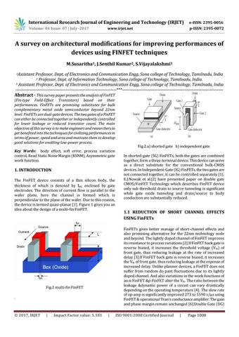
1. INTRODUCTION The FinFET device consists of a thin silicon body, the thickness of which is denoted by tsi, enclosed by gate electrodes. The direction of current flow is parallel to the wafer plane, here the channel is formed which is perpendicular to the plane of the wafer. Due to this reason, the device is termed quasi-planar [1]. Figure 1 gives you an idea about the design of a multi-fin FinFET.
.
|
Impact Factor value: 5.181
In shorted-gate (SG) FinFETs, both the gates are combined together, form a three-terminal device. This device can serve as a direct substitute for the conventional bulk-CMOS devices. In Independent-Gate (IG) FinFETs, the two gates are not connected together, it can be controlled separately [1]. E.J.Nowak et al.[2] have presented paper on double gate CMOS/FinFET Technology which describes FinFET device only sub threshold drain to source tunneling is significant while gate oxide tunneling and drain/source to body conduction are substantially reduced.
1.1 REDUCTION OF SHORT CHANNEL EFFECTS USING FinFETs FinFETs gives better manage of short-channel effects and also promising alternative for the 22nm technology node and beyond. The lightly doped channel of FinFET improves its resistance to process variations [2].If FinFET back gate is reverse biased, it increases the threshold voltage (Vth) of front gate, thus reducing leakage at the rate of increased delay [3].If FinFET back gate is reverse biased, it increases the Vth of front gate, thus reducing leakage at the expense of increased delay. Unlike planner devices, a FinFET does not suffer from random do pant fluctuations due to its lightly doped channel. And also variations in the work functions of an n-FinFET &p-FinFET alter the Vth. The ratio between the leakage &dynamic power of a circuit can vary drastically depending on the operating temperature [4]. The slew rate of op-amp is significantly improved 273 to 5590 v/µs using FinFET & operational Tran’s conductance amplifier. The gain and phase margin remain unchanged [6].Double Gate (DG)
Fig.1 multi-fin FinFET
© 2017, IRJET
Fig.2.a) shorted gate b) independent gate
|
ISO 9001:2008 Certified Journal
|
Page 1008