International Research Journal of Engineering and Technology (IRJET)
e-ISSN: 2395-0056
Volume: 04 Issue: 07 | July -2017
p-ISSN: 2395-0072
www.irjet.net
Different leakage power reduction techniques in SRAM Circuits: A State-of-the-art Review Chetan1, Prachi Chaudhary2, Pawan Kumar Dahiya3 1Scholar
of M. Tech. in ECE (VLSI Design), Deenbandhu Chhotu Ram University of Science & Technology, Sonepat, India 2,3 A.P., ECED, Deenbandhu Chhotu Ram University of Science & Technology, Sonepat, India --------------------------------------------------------------------------***-------------------------------------------------------------------------
Abstract - In today’s electronic devices, memory is a most important part that shares a major part of total circuit power. With the newer technology size of processing data is increasing which results in increase of memory and overall circuit size. The stored data is affected by the leakage power. There is a major power loss due to the leakage current. The leakage power loss is inversely proportional to size of the circuit which is undesired. The different leakage power reduction technique has been developed to overcome this problem. This paper presents the study of various leakage current in CMOS devices and the reduction techniques used to overcome this problem. In this paper a newer technique called lector (Leakage Control Transistor Technique) is explained.
OFF state in a path between high to low voltage is less leaky compare to only one transistor OFF between any supply and ground path”.
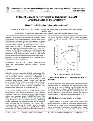
KEYWORDS: CMOS, (LECTOR) Leakage Control Transistor, SRAM cell, Sub-threshold, Leakage Current, Threshold voltage. 1. INRODUCTION In last few years to accomplish the high performance CMOS device, scaling is used. As a result of scaling the delay and area of device are reduced. Additionally, a scaled device also has low supply voltage, reduced threshold voltage, gate oxide thickness and channel length which improves the performance of device. But the minimization of these features inversely affects the leakage current .as technology is scaled down, the leakage current becomes comparable with dynamic power dissipation. As shown in Fig -1. [10] To reduce the leakage current of CMOS devices various techniques are used. These techniques are sleep transistor technique, Forced stack technique, Sleepy stack technique and the latest technique named as LECTOR technique. These techniques reduces the leakage by stacking leakage path using the off transistors. In LECTOR technique the leakage control transistors are used in between pull-up and pulldown network. In this technique one leakage control transistors is always near its cut-off region of operation without depending on of the input voltage. The Lector follows the concept that, “a state with more than one transistor in
© 2017, IRJET
|
Impact Factor value: 5.181
|
Fig-1: Power dissipation vs technologies
2. DIFFERENT LEAKAGE CURRENTS IN MOSFET DEVICES: In a CMOS transistor there are two types state of working 1) Non-conducting 2) Conducting. In non-conducting state, there are three types of leakage currents which are subthresold leakage current, gate induced drain leakage current and punch through current.[2] In conducting state two leakage currents are gate tunnelling current and junction leakage current. All leakage currents are shown in fig -2.
2.1 DIBL (Drain Induced Barrier Lowering): As higher voltage is applied on the drain terminal the depletion region of drain start interfacing with the source terminal. Due to this the barrier potential between drain and source is lowered. At this lower potential barrier charge carriers are injected by source without any effective role of
ISO 9001:2008 Certified Journal
| Page 742