International Research Journal of Engineering and Technology (IRJET)
e-ISSN: 2395 -0056
Volume: 04 Issue: 06 | June -2017
p-ISSN: 2395-0072
www.irjet.net
FPGA based implementation of Cascaded H-Bridge Five Level Inverter Mr. Amarsinha Ranaware1, Prof. S. R. Jagtap2 1PG student, RIT Sakharale Professor, E&TC Dept., RIT Sakharale (MS), India ---------------------------------------------------------------------***--------------------------------------------------------------------2Associate
Abstract – This paper presents Single phase cascaded
blocks. FPGA also support modification as per requirement. This feature of reprogramming capability of FPGA makes it suitable to make the design using FPGA.
H-bridge five level inverter. The simulation is done by using Matlab-Simulink which gives five level output. The control signals for this H-Bridge multilevel inverter are implemented by using FPGA controller based on PWM signal i.e. modulation technique and digital technique. The advantage of multilevel Inverter is 1-lower voltage stress, 2-higher efficiency 3-lower electromagnetic interference. FPGA is used for the hardware implementation. The reason is 1- its high computation speed that can ensure the accuracy of the instants that gating signals are generated. A Multilevel inverter achieves High power rating and improves performance of the system. As numbers of steps or levels are increased the output is reaches to near sine wave. Thus results in low harmonics.
This paper presents a multilevel PWM inverter having five level output voltage. MATLAB-Simulink is used for simulation of the model and Xilinx Web Pack software is used to generate PWM pattern. The final design is implemented on Xilinx FPGA (XC3S400PQ208) from Spartan 3.
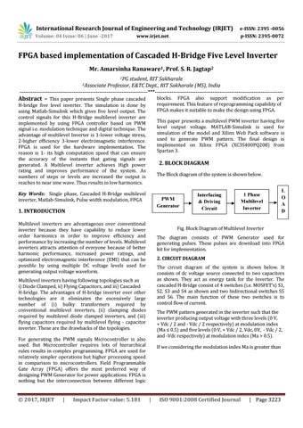
2. BLOCK DIAGRAM The Block diagram of the system is shown below.
Key Words: Single phase, Cascaded H-Bridge multilevel inverter, Matlab-Simulink, Pulse width modulation, FPGA
PWM Generator
1. INTRODUCTION Multilevel inverters are advantageous over conventional inverter because they have capability to reduce lower order harmonics in order to improve efficiency and performance by increasing the number of levels. Multilevel inverters attracts attention of everyone because of better harmonic performance, increased power ratings, and optimized electromagnetic interference (EMI) that can be possible by using multiple DC voltage levels used for generating output voltage waveform.
Impact Factor value: 5.181
L O A D
The diagram consists of PWM Generator used for generating pulses. These pulses are download into FPGA kit for implementation. 2. CIRCUIT DIAGRAM The circuit diagram of the system is shown below. It consists of dc voltage source connected to two capacitors as shown. They act as energy tank for the Inverter. The cascaded H-Bridge consist of 4 switches (i.e. MOSFET’s) S1, S2, S3 and S4 as shown and two bidirectional switches S5 and S6. The main function of these two switches is to control flow of current. The PWM pattern generated in the inverter such that the inverter producing output voltage with three levels (0 V, + Vdc / 2 and - Vdc / 2 respectively) at modulation index (Ma ≤ 0.5) and five levels (0 V, + Vdc / 2, Vdc, 0V, - Vdc / 2, and -Vdc respectively) at modulation index (Ma > 0.5).
For generating the PWM signals Microcontroller is also used. But Microcontroller requires lots of hierarchical rules results in complex programming. FPGA are used for relatively simpler operations but higher processing speed in comparison to microcontrollers. Field Programmable Gate Array (FPGA) offers the most preferred way of designing PWM Generator for power applications. FPGA is nothing but the interconnection between different logic
|
1 Phase Multilevel Inverter
Fig. Block Diagram of Multilevel Inverter
Multilevel inverters having following topologies such as i) Diode Clamped, ii) Flying Capacitors, and iii) Cascaded H-bridge. The advantages of H-bridge inverter over other technologies are it eliminates the excessively large number of (i) bulky transformers required by conventional multilevel inverters, (ii) clamping diodes required by multilevel diode clamped inverters, and (iii) flying capacitors required by multilevel flying - capacitor inverter. These are the drawbacks of the topologies.
© 2017, IRJET
Interfacing & Driving Circuit
If we considering the modulation index Ma is greater than
|
ISO 9001:2008 Certified Journal
| Page 3223