International Research Journal of Engineering and Technology (IRJET)
e-ISSN: 2395 -0056
Volume: 04 Issue: 01 | Jan -2017
p-ISSN: 2395-0072
www.irjet.net
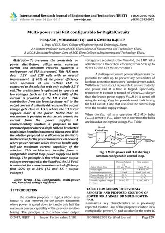
Multi-power rail FLR configurable for Digital Circuits P.RAJASRI1 , MOHAMMAD TAJ2 and K GOVINDA RAJULU3 1. Dept. of ECE, Eluru College of Engineering and Technology, Eluru. 2. Assistant Professor, Dept. of ECE, Eluru College of Engineering and Technology, Eluru. 3. HOD & Associate Professor, Dept. of ECE, Eluru College of Engineering and Technology, Eluru. ---------------------------------------------------------------------***--------------------------------------------------------------------voltages are required at the NanoPad, the 1.8V rail is Abstract— To overcome the constraints on activated for a theoretical efficiency from 55% up to power distribution, silicon area, quiescent 83% (1.0 and 1.5V output voltages). current and minimum required efficiency, a multi-power rail FLR is proposed. This FLR uses A challenge with multi power rail systems is the dual 1.8V and 3.3V rails with an overall potential for latch up. To prevent any possibilities of improvement of 40% of the power efficiency latch up, protection transistors (switches) were added. when operating at low voltage (1.0 V) With these transistors,it is possible to ensure that only compared to the solution with only a single 3.3 V one power rail at a time is tapped. Specifically, rail. The architecture i s optimized to operate at transistors M14 must be turned off when VOUT is larger low voltages (such as 1.0 V) where 80% of the than the branch power supply VDDn.M14 is turned off current is provided by the 1.8 V rail. This using the voltage VBASE that provides static bulk biasing contribution from the lowest voltage rail to the for M13 and M14 and that also feed the control loop output current drastically decreases as the output with the suitable supply voltage. voltage gets close to 1.5 V, where the 3.3 V rail supplies most of the power. Notice that no When the VDDn rail is in operation M13-M14 bulks mechanism is provided in this circuit to limit the (VBASE) are set to VDDn. When not in operation the bulks current from the power supplies. A are biased at the highest voltage,Vdd1. Table complementary solution is proposed in this presented paper where a single rail can be selected to minimize heat dissipation and silicon area. With the solution proposed as a silicon area similar to that reserved for the power transistors will be used, where power rails are scaled down to handle only half the maximum current capability of the solution. This architecture benefits from a Fig. 1 Multi-power rail FLR sharing a configurable control loop, power supply and bulk common configurable control loop. biasing. The principle is that when lower output voltages are required at the NanoPad, the 1.8 V rail is activated for a maximum theoretical efficiency from 55% up to 83% (1.0 and 1.5 V output voltages). Index Terms—FLR, Configurable, multi-power rail, NanoPad, voltage regulator. TABLE I COMPARISON OF REVIOUSLY REPORTED AND PROPOSED SOLUTION OF POWER FOR A SINGLE OR MULTI-POWERRAIL summarizes key characteristics of a previously reported solution and of the proposed solution for a configurable power I/O pad suitable for the wafer IC
1 INTRODUCTION the solution proposed in fig-1,a silicon area similar to that reserved for the power transistors where power is scaled down to handle only half the maximum current capability of the previous solution biasing. The principle is that when lower output © 2017, IRJET
|
Impact Factor value: 5.181
|
ISO 9001:2008 Certified Journal
|
Page 329