International Research Journal of Engineering and Technology (IRJET)
e-ISSN: 2395 -0056
Volume: 04 Issue: 01 | Jan -2017
p-ISSN: 2395-0072
www.irjet.net
Review of Relay Processes and Design Optimization for Low Voltage Operation Soumitra S Pande1, Sanjeev Gupta2 1Research
2Professor
Scholar, ECE Department, AISECT University, Bhopal (M.P.) India & Head, ECE Department, AISECT University, Bhopal (M.P.) India
---------------------------------------------------------------------***--------------------------------------------------------------------2. 5 MASK/7 MASK PROCESS Abstract - This paper focuses on relay process and design optimization. With optional additional lithography steps, we can achieve a more robust process required for eventual device scaling, highly reduced device footprint area, and the ability to form interconnects to fabricate circuits. Improved relay designs minimize parasitic electrostatic force issues and enhance functionality. The process flow is optimized to achieve the lowest switching voltages, while still ensuring reliable turn-off and avoiding stiction. New device concepts increase device functionality to reduce the number of structures required to achieve a certain function, and provide a new paradigm for designing circuits using relays.
Key Words: electrostatic force, digital integrated circuits, lithography, interconnects, parasitic effects, stiction.
1.INTRODUCTION The ideal switching characteristic of zero off-state leakage and abrupt switching behavior of relays makes it attractive for DIC (digital integrated circuit) applications as chip power density has become a major challenge in recent years. A robust and reliable 4Terminal (4T) relay technology, having high yield (>95%) and excellent endurance (>1010 on/off cycles) has been demonstrated previously (1). Indeed, ideal switching characteristic is demonstrated with SS < 0.1mV/dec and immeasurably low IOFF (<10-14A). However, the process technology and design are not optimized. The device footprint is unnecessarily large, and the release process relies on a timed etch. Parasitic electrostatic effects were found and operating voltages remain too large, making it difficult to implement complex logic circuits with the technology. In order to fully realize the promise of relays as an alternative to CMOS for low power digital circuits, the relays need to be able to operate with voltages <1 V, i.e. with minimal hysteresis. The hysteresis voltage sets the minimum VPI where the relays can still turn off (i.e. when VRL=0V, VPI = hysteresis voltage).
© 2017, IRJET
|
Impact Factor value: 5.181
|
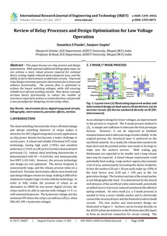
Fig -1: Layout view (1) illustrating improved anchor and interconnect design on dual source/drain devices. (a) An inverter circuit. (b) Device anchored directly on W (M1 interconnect). As an attempt to design for lower voltages, an improvement to the process is required. The 4-mask process studied in (1), is simple and sufficient to fabricate the first prototype devices. However, it can be improved to facilitate miniaturization and to fabricate large circuits reliably. In the original process, the structural layer is anchored on the sacrificial material. As a result, the release time needs to be kept short and the printed anchor size needs to be large to make sure the anchors survive. With scaling, gap thicknesses are expected to be smaller and a long release time may be required. A timed release requirement could potentially limit scaling. Large anchor regions also consume a lot of area, unnecessarily increasing the device footprint. In fact, the anchors (50 μm × 50 μm each) make up >50% of the total device area (120 μm × 150 μm) in the 1st generation design. The location and size of the actual anchor is not lithographically fixed. It is determined by the lateral etch distance of the sacrificial oxide underneath, potentially an added source of process-induced variation in the effective spring constant. An extra mask (i.e. a 5-mask process) is needed to form a more reliable anchor and to electrically connect the structural layer and the fixed electrodes to build circuits. The new anchor and interconnect design are illustrated in Figure 1. Anchors can be formed directly on the Al2O3 substrate dielectric or the W electrodes (M1 layer) to form an electrical connection for circuit routing. The ISO 9001:2008 Certified Journal
|
Page 1298