International Research Journal of Engineering and Technology (IRJET)
e-ISSN: 2395 -0056
Volume: 03 Issue: 12 | Dec -2016
p-ISSN: 2395-0072
www.irjet.net
OCTABAND MICROSTRIP PATCH ANTENNA USING DGS FOR S-BAND, C-BAND & X-BAND APPLICATIONS K. Pradeep Rajashekar 1M.Tech
Student, Dept. of ECE, St. Ann’s College of Engineering and Technology, Andhra Pradesh, India
---------------------------------------------------------------------***---------------------------------------------------------------------
Abstract - A miniature version of octaband antenna is
In this paper, an octaband antenna is designed incorporating a rectangular slot on the radiating patch since it enhances the overall performance of the antenna [5]. In reference [6], dual band monopole antenna is achieved using rectangular DGS structures and in reference [7], triple band antenna is achieved using DGS structure and L-shaped slots on the patch. Similar multiband antennas are designed in references [9-11] by etching slots on the monopole structures. The proposed antenna also consists of two L-shaped slots on opposite edges of the ground plane resulting in defective ground structure. The substrate used for the simulation is FR4 having dielectric constant of 4.4 and loss tangent of 0.02.The size of the antenna is a major concern especially for mobile applications with regard to the space available on the devices[12]. The process of miniaturization is kept in mind while designing the proposed antenna making it suitable to be embedded in to smaller areas.
Key Words: Multiband antenna, Octaband, HFSS, DGS, S-band, C-band, X-band, Microstrip patch antenna.
2. ANTENNA DESIGN
proposed for various communication applications in S-band, C-band and X-band. The proposed antenna has a defective ground structure (DGS) to improve the performance of the antenna. The ground plane has L-shaped slots and the patch consists of a rectangular slot to enable multi frequency band operation. This antenna is designed on FR4 substrate with dielectric constant 4.4, thickness 2 mm with dimensions of 40 X 40 X 2 mm3.The design of the structure and result analyzation is carried out using High Frequency Structural Simulator (HFSS) software. The proposed antenna exhibits return loss of -24dB, -21dB, -13dB, -16dB, -19dB, -15dB, -12dB, -15dB at 3.2GHz, 4.6GHz, 5.6GHz, 6.6GHz, 8.1GHz, 9.1GHz, 10.1GHz, 11.6GHz respectively with VSWR < 2 for all the eight bands. The observed results suggest that the proposed antenna can be employed for multiple wireless communication applications.
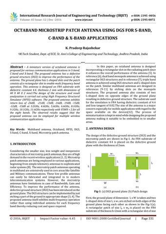
The design of the defective ground structure (DGS) and the microstrip patch are shown in Fig-1. An FR4 substrate of dielectric constant 4.4 is placed on the defective ground plane with the thickness of 2mm.
1. INTRODUCTION Considering the smaller size, less weight and inexpensive characteristics of microstrip patch antennas, they are of high demand in the recent wireless applications [1, 2]. Microstrip patch antennas are being employed in various applications, beginning from simple telemetry antennas to sophisticated radar systems [8]. The microstrip patch antennas operating in multiband are extensively used in core areas like Satellite and Military communications. These low profile antennas can easily be fabricated and integrated in to modern telecommunication systems. However, the microstrip antennas have limitations in case of Bandwidth, Gain and Efficiency. To improve the performance of the antenna, defective ground structure (DGS) has been introduced on the ground plane. The DGS structure can be implemented by just etching a part of the ground in appropriate shape [3, 4]. The proposed antenna itself exhibits multi frequency operation rather than using individual antenna for each frequency band thereby reducing cost and space required.
Š 2016, IRJET
|
Impact Factor value: 4.45
Fig-1: (a) DGS ground plane (b) Patch design First, the ground plane of dimension L x W is taken and two L-shaped slots of size l1 x w1 are etched on both edges of the ground plane facing each other as shown in the Fig-1(a). A rectangular patch of size lp x wp is placed on the FR4 substrate of thickness h=2mm with a rectangular slot of size
|
ISO 9001:2008 Certified Journal
|
Page 331