
International Research Journal of Engineering and Technology (IRJET) e-ISSN: 2395-0056
Volume: 11 Issue: 05 | May 2024 www.irjet.net p-ISSN: 2395-0072
International Research Journal of Engineering and Technology (IRJET) e-ISSN: 2395-0056
Volume: 11 Issue: 05 | May 2024 www.irjet.net p-ISSN: 2395-0072
Einesh Naik1 , Prof. Nadine Dias2
1Student, Department of Information Technology and Engineering, Goa College of Engineering, Farmagudi, Goa, India
2Assistant Professor, Department of Information Technology and Engineering, Goa College of Engineering, Farmagudi, Goa, India
Abstract - This work presents a deep learning system that uses the principle of the You Only Look Once (YOLO) methodology to perform PCB (printed circuit board) quality inspections. Deep learning algorithms have been widely used in many different fields because of their remarkable efficiency and accuracy. Comparably, there has been a lot of interest in the accurate detection of PCB flaws using deep learning techniques, such as the You Only Look Once (YOLO) method. The synthetic dataset from Kaggle was used in the suggested strategy. 1386 pictures representing 6 PCB flaws make up the dataset. Defects include missing holes, mouse bites, open circuits, short circuits, spurious copper, and shorts arepresent in the dataset. A YOLOv8X model is then trainedusingthedata to identify PCB flaws With a batch size of 16, the suggested model successfully identified defects in PCBs with 97.9% accuracy.
Key Words: YOLO; deep learning; printed circuit board; printed wiring board; missing hole; mouse bite; open circuit; short, spur; spurious copper
1.INTRODUCTION
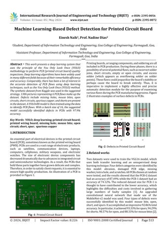
Anessentialpartofelectricaldevicesistheprintedcircuit board(PCB),sometimesknownastheprintedwiringboard (PWB).PCBsareusedinavastrangeofelectronicproducts, such as satellites, communication devices, laptops, computers, cellphones, military weapons, and electronic watches. The size of electronic device components has decreaseddramaticallyduetoadvancesinintegratedcircuit andsemiconductortechnologies.Asaresult,thePCBsthat holdthesepartstogetherhavegrowndelicateandcomplex. Therefore,inordertosatisfyclientrequests,itisessentialto ensurehigh-quality production. An illustration of a PCB is providedinFigure1.
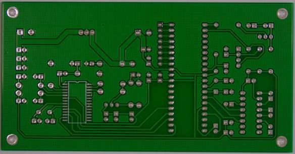
Printingboards,arrangingcomponents,andsolderingareall includedinPCBproduction.Duringthesephases,thereisa possibilityofseveralpotentialflaws,suchasincorrectsolder joins, short circuits, empty or open circuits, and excess solder (which appears as overflowing solder on solder points).Theseflawscouldjeopardizetheboard'sstabilityor perhaps cause the board to break entirely. Thus, it is imperative to implement a highly effective and precise automatic detection module for the purpose of examining variousflawsduringthePCBmanufacturingprocess.Figure 2illustratesexamplesofsurfacedefectsinPCBs.
Two datasets were used to train the VGG16 model, which uses both transfer learning and an unsupervised deep learningtechnique.Fourdefectcategorieswereidentifiedby this model: abrasion, damaged PCB edge, missing washer/extrahole,andscratches.60PCBschosenatrandom weretested,andtheresultsshowedthatthePCB-Gdataset hadanaccuracyof87.49%whilethePCB-1datasethadan accuracyof74.12%.ThereduceddatasetsizeforPCB-1is thought to have contributed to the lower accuracy, which highlights the difficulties and costs involved in gathering large numbers of faulty samples [1]. An upgraded convolutional neural network that made use of the MobileNet-v2model wasused.Fourtypesofdefectswere successfully identified by this model: mouse bite, open, short,andspurs.Itaccomplishedanimpressive92.86%total accuracy.Inparticular,itachieved93.33%forspurs,94.29% forshorts,98.57%foropen,and88.33%formousebites[2].
Volume: 11 Issue: 05 | May 2024 www.irjet.net p-ISSN: 2395-0072
3.1 Dataset overview
ThedatasetmustfollowthePascalVOCformatforYOLOv8 to work properly, and each image must have a matching annotationfileinthe.txtformat.TrainandValidatesubsets shouldbecreatedfromthedataset.
The dataset used in this experiment was obtained from Kaggle. 1386 photos with six different types of defects missing hole, mouse bite, open circuit, short, spur, and spurious copper are included in this freely accessible synthetic PCB dataset. The inclusion of these flaws makes detectionandclassificationtaskseasier.
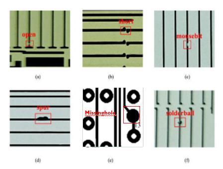
TheYOLOv8real-timeobjectdetectoristhemostadvanced model in the YOLO series, offering state-of-the-art performanceintermsofaccuracyandspeed.Byintroducing novel features and improvements, YOLOv8 builds on the innovations of its predecessors and proves to be a strong optionforavarietyofobjectidentificationtasksinawide rangeofapplications.
YOLOv8'sarchitectureisanextensionoftheYOLOalgorithm series'earliermodels.Itmakesuseofaconvolutionalneural network,whichconsistsoftheheadandthebackbone.The foundationofYOLOv8isbuiltusingamodifiedversionofthe CSPDarknet53 architecture, which has 53 convolutional layers and cross-stage partial connections to improve the informationflowbetweenthelayers.Multipleconvolutional layersatthefrontofYOLOv8arefollowedbyfullyconnected layers,andtheirjobistopredictboundingboxes,objectness scores, and class probabilities for objects that are discovered. The addition of a self-attention mechanism to thenetwork'sbrainisnoteworthysinceitenablesthemodel tofocusonvariousareasoftheimageandmodifytheweight ofvariablesaccordingtotheirsignificance.
Besides these characteristics, YOLOv8 uses a feature pyramidnetworktoachievesuperiorperformanceinmultiscaledobjectdetection. The model candetectthingsin an image,nomatterhowbigorlittle,becausethisnetworkhas numerouslayersthatarespecificallybuilttodetectobjects atdifferentscales.
To determine the weights, the PCB-YOLO model was subjectedtoseveraltrainingcyclesonthetrainingset.The testset'simageswereusedtotestthemodelusingtheideal weightsthatweredeterminedduringthetrainingphase.The experimentalfindingsshowthatthemeanaverageprecision (mAP) of 0.995 for the detection of missing holes is quite good. The unique characteristics and fewer diversified shapesassociatedwithmissingholesarethereasonforthis performance.Similartospuriouscopper,opencircuits,and shorts have high mAP values because of their decreased vulnerability to other flaws and background interference. Due to their physical similarities, spur and mouse bite defectscanbedifficulttoidentifyfromoneanother,which couldresultinmisidentificationsoncetheregionaldensity reaches a certain point. In spite of this intricacy, the PCBYOLO-v8 model is able to detect all six flaws with a mean averageprecisionof0.979.
International Research Journal of Engineering and Technology (IRJET) e-ISSN: 2395-0056
Volume: 11 Issue: 05 | May 2024 www.irjet.net p-ISSN: 2395-0072
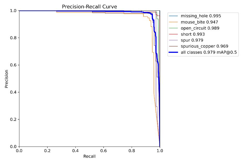
Chart -1:PrecisionRecallCurve
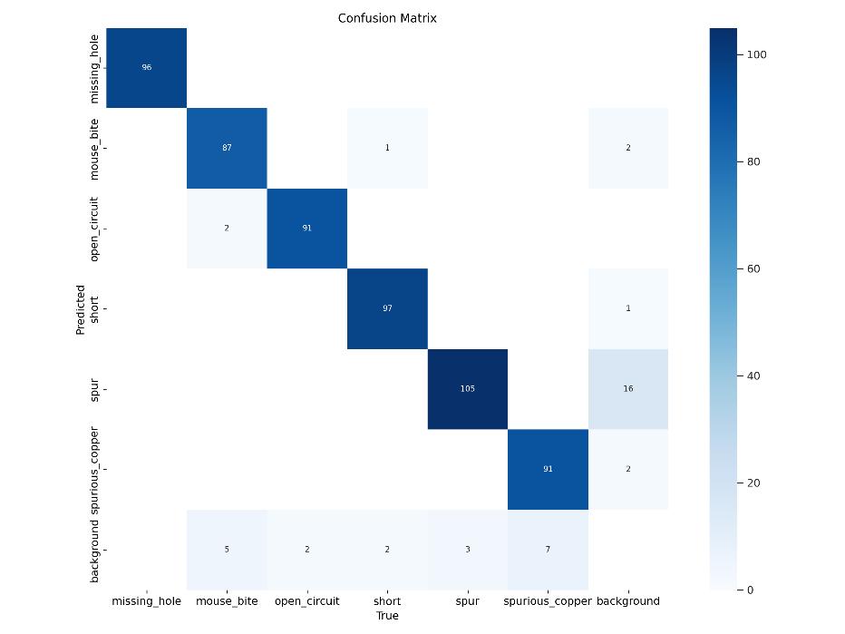
Chart -2:ConfusionMatrix
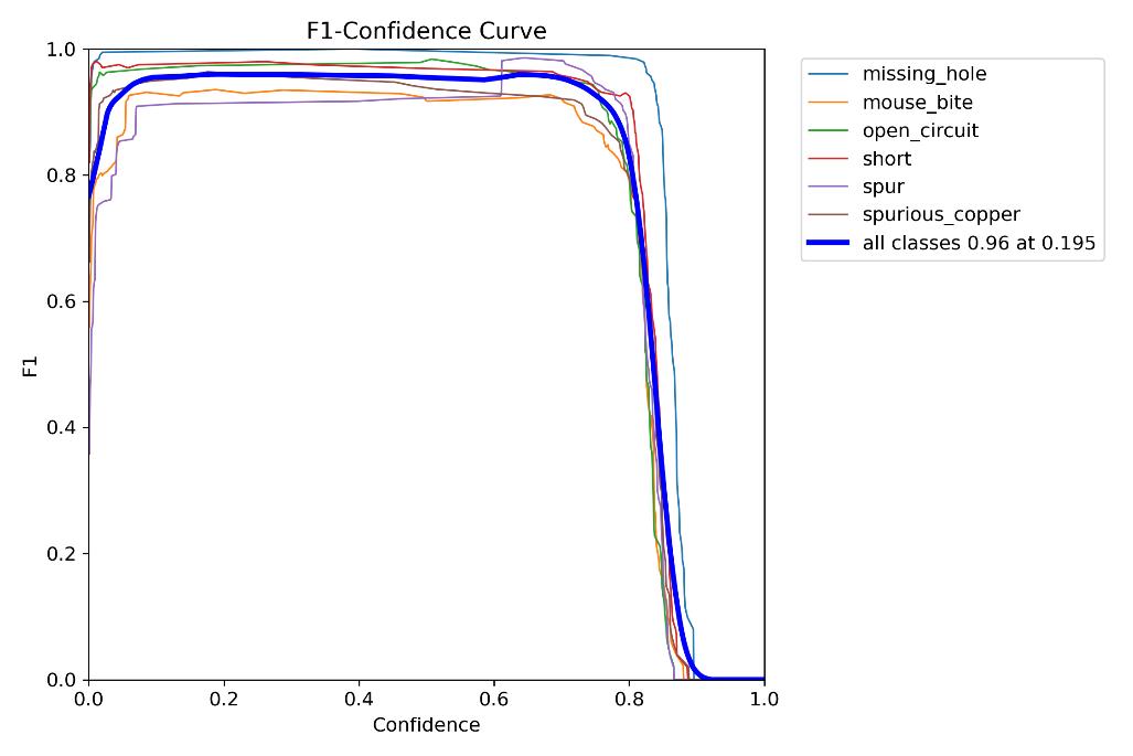
Chart -3:F1-ConfidenceCurve
PCB devices, which are essential parts of many different electronicproducts,havesignificantlyimprovedhumanlife. Production and sorting processes can be accelerated by effectively classifying and detecting defects in PCB image data.ThisdevelopmentaddressestherisingneedforPCBs while also increasing production and recycling efficiency. Significanteffortshavebeenmadebyindustryandacademic organizations to improve PCB defect detection and categorization. In this work, we provide YOLOv8, an inventive single-shot object identification model designed especially for PCB fault classification. With an overall accuracy of 97.9%, our model is very effective when comparedtoothermodelsthatarecurrentlyinuse.
However, this study acknowledges significant limitations thatprovideuppossibilitiesforfurtherinvestigation.Since thedatasetusedinthisstudyissynthetic,moreresearchis needed to determine how well our method functions on actualPCBs.In-depthresearchandvalidationaretherefore requiredtoguaranteethemodel'scorrectnessandsuitability foruseinpracticalsituations.
[1] Detection Defect in Printed Circuit Boards using Unsupervisedfeatureextractionupontransferlearning, Volkau Ihar, Abdul Mujeeb, Dai Wenting, Erdt Marius, Sourin Alexei, 2019 International Conference on Cyberworlds(CW),©IEEE2019.
[2] PrintedCircuitBoardsDefectDetectionMethodBased on Improved fully Convolutional Networks, Jianfeng Zheng, Xiaopeng Sun, Haixiang Zhou, Chenyang Tian, Hao Qiang, 10.1109/ACCESS.2022.3214306 © IEEE 2022.
[3] DetectionofPCBsurfacedefectswithimprovedfasterRCNN and feature pyramid network, Bing Hu, Jianhui Wang,10.1109/ACCESS.2020.3001349©IEEE2020.
[4] Yolov4-MN3forPCBsurfacedefectdetection,Xinting Liao,ShengpingLv,DenghuiLi,YongLuo,ZichunZhu, Chengjiang,10.3390/app112411701©MDPI2021.
[5] PrintedCircuitBoardDefectDetectionMethodsBased on Image Processing, Machine Learning and Deep Learning: A Survey, Qin Ling, Nor Ashidi Mat, 10.1109/ACCESS.2023.3245093©IEEE2023.
[6] PCB Defect Detection Based on Deep Learning Algorithm, Chun Chen, Rey-Chue Hwang, Huang-Chu Huang,10.3390/pr11030775©MDPI2023.
[7] LPViT: A Transformer Based Model for PCB Image Classification and Defect Detection, Kang AN, Yanping Zhang,10.1109/ACCESS.2022.3168861©IEEE2022.
International Research Journal of Engineering and Technology (IRJET) e-ISSN: 2395-0056
Volume: 11 Issue: 05 | May 2024 www.irjet.net p-ISSN: 2395-0072
[8] Feature-Learning-Based Printed Circuit Board InspectionviaSpeeded-UpRobustFeaturesandRandom Forest, Eun Hye Yuk, Seung Hwan Park, Cheong-Sool Park, Jun-Geol Baek, 10.3390/app8060932 © MDPI 2018.
[9] Defect Detection in Printed Circuit Boards Using YouOnly-Look-OnceConvolutionalNeuralNetworks,Venkat Anil Adibhatla, Huan-Chuang Chih, Chi-Chang Hsu, Joseph Cheng, Maysam F. Abbod, Jiann-Shing Shieh, 10.3390/electronics9091547©MDPI2020.
[10] DefectDetectioninPrintedCircuitBoardsUsingSemiSupervised Learning, Thi Tram Anh Pham, Do Kieu Trang Thoi, Hyohoon Choi, Suhyun Park, 10.3390/s23063246©MDPI2023.