
International Research Journal of Engineering and Technology (IRJET) e-ISSN:2395-0056
Volume: 11 Issue: 05 | May 2024 www.irjet.net p-ISSN:2395-0072
International Research Journal of Engineering and Technology (IRJET) e-ISSN:2395-0056
Volume: 11 Issue: 05 | May 2024 www.irjet.net p-ISSN:2395-0072
K.G.Venkata
Krishna1,
N.K.KamalaDevi
2, K.Vishnu Varma3, A.Yedukondalu4
1 Assistant Professor, Department of Electronics and Communication Engineering, Krishna University College of Engineering and Technology Krishna University, Machilipatnam Andhra Pradesh, India
2UG Student, Dept. of ECE, Krishna University College of Eng. &Tech, Machilipatnam, A.P, India.
3UG Student, Dept. of ECE, Krishna University College of Eng. &Tech, Machilipatnam, A.P, India.
4UG Student, Dept. of ECE, Krishna University College of Eng. &Tech, Machilipatnam, A.P, India.
Abstract - The Re prefers a more condensed, straightforward set of instructions that all execute in the same amount of time. This processor preserves functional units without compromising performance. The design makes advantage of an architecture known as Harvardd, which includes separate data and instruction memory. A word of instructions has 24 bits in total. The CPU supports three addressing modes in addition to sixteen instructions. It contains sixteen general-purpose registers. Any register has the capacity to store 16 bits of data. The procedure performs 11 arithmetic and logical operations. Every module is developed and tested separately at every stage of implementation before being properly mapped into the toplevel module. The simulation results are verified using Xilinx Vivado 2023.1 once the design input and synthesis are finished using the same tool.
Key Words: RISC, 16-bit, VLSI, verilog
1.INTRODUCTION
When the performance of CISC fell short of expectations and the controller design grew more challenging, people startedtoconsideralternateapproaches.Ithasbeenfound that when a CPU interfaces with memory, speed is lost. Reducingthecomplexityoftheinstructionsetwastheonly option to raise CPI. Simpler in terms of design than in termsoffunctioning.Asaresult,theCPUisnotrequiredto accessmemoryforverymanyinstructionsinatypicalRISC architecture probably only load and store. Ultimately, pipelining increased performance. Only a few additional registers can provide a new level of performance by lowering CPU and increasing throughput. Consequently, the instruction may be successfully executed in one clock cycle. It's a common misperception that when the term "Reduced Instruction Set Computer" is used, instructions areonlyremovedtocreateasmallersetofinstructions.In fact,RISCinstructionsetshavegrowninsizeovertime,and several of them now include more instructions than many CISCCPUs.
2.1 S. Lad and V. S. Bendre, "Design and Comparison of Multiplier using Vedic Sutras," 2019 5th International Conference On Computing, Communication, Control And Automation(ICCUBEA), Pune,India,2019, pp.1-5
Fast processing units are necessary for many real-time applications in modern computerized era. The basic building elements of these units are ALU and MAC, which are necessary for quick and effective execution. Digital signal processors primarily use multipliers as their primary component. ALU and MAC performance can be improved by modifying registers, multiplier, and adder to retain correctness and speed up execution. Due to the growing delays restrictions, the design of quicker multipliersisprioritizedforimplementationinprocessors. It is crucial to create quicker multipliers in order to increasemultiplicationspeed.
2.2 Balpande Vishwas V, Abhishek B. Pande, Meeta J. Walke, BhavnaD. Choudhari and Kiran R. Bagade. “Design and Implementation of 16 Bit ProcessoronFPGA.”(2015).
Thisprojectinvolvesthedesignofa16-bitRISCprocessor and the Verilog HDL modeling of its constituent parts. Harvard architecture is the basis of the processor. This instruction set's extreme simplicity provides an indication of the sort of hardware that should be able to correctly execute the set of instructions. More sophisticated blocks likeanALUandmemoryhavebeen builtandsimulatedin addition to the sequential and combinational processor building blocks like adders and registers. In this project, comprehensive structural ALU modeling, beginning with half adders, has been completed. Ultimately, the semicustomlayoutwascreatedjustforALU.
2.3 Seung Pyo Jung, Jingzhe Xu, Donghoon Lee, Ju Sung Park, Kang-joo Kim and Koon- shik Cho, "Design & verification of 16 bit RISC processor,"
International Research Journal of Engineering and Technology (IRJET) e-ISSN:2395-0056
Volume: 11 Issue: 05 | May 2024 www.irjet.net p-ISSN:2395-0072
2008 International SoC Design Conference, Busan,2008, pp.III-13-III-14
Thisarticlepresentsthedesignandverificationprocessfor a 16-bit RISC processor. The suggested processor features a Harvard design, with internal debug logic, a 5-stage pipeline for instruction execution, and a 24-bit address. The FPGA-based processorsuccessfullyexecutes the SOLA algorithm and the ADPCM vocoder. Personal digital assistants(PDAs)andportablemultimediaplayers(PMPs) are not unique human inventions. Thus, SOC level ASICs (ApplicationSpecificIntegratedCircuits)areusedtocreate compact and low power processors. The 8051 and ARM 7 processors are the most widely used SOC level ASIC processors.
2.4 Chandni N. Naik, Vaishnavi M. Velvani, Pooja J. Patel, Khushbu G. Parekh, "VLSI Based 16 Bit ALU with Interfacing Circuit", International Journal of Innovative and Emerging Research in Engineering Volume 2, Issue 3, 2015.
This project uses VHDL to construct a 16-bit ALU that is interfacedwithROMandRAM.OneofthemostcrucialCPU modules, the ALU allows for modifications to be made during the majority of instruction executions. Therefore, furtherALUoperationisacrucial duty.Afterthat,Xilinxis used to implement this design. After creating an ALU, interfacedRAMandROMwithit.Waveformsaredisplayed foreachresultintheXilinxprogram.TheCPUisspedupby thisproject.
2.5 Pushpalata Verma, K. K. Mehta, “Implementation of an Efficient Multiplier based on Vedic Mathematics Using EDA Tool”, InternationalJournalof Engineering and Advance Technology, Vol.1, no. 5, June,2012
An optimized area efficient multiplier is built in this project. Due to the increasing growth of integration, many significantsignal processingsystemsaredesignedonVLSI platforms. Systems and applications for signal processing needalotofprocessingpower,whichmeanstheyconsume a lot of energy. Performance and area are two crucial design factors for VLSI systems. In general, the multiplier element's performance determines the system's performance.
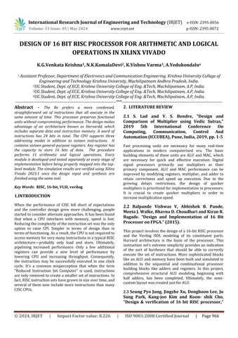
The processor's job is to efficiently carry out each and every instruction provided in accordance with machine language. Arithmetic and Logical Unit, or ALU, is a combinationalcircuit.Thisunitismadetoexecutedifferent integerswithdifferentsetsofinstructions.Operationcode (opcode) plus a few operands make up the instruction (machine word) that an ALU receives from a processor.
Thus,theoperandsareemployedintheoperationafterthe opcode instructs the ALU on which and what operation to carry out. A little collection of data storage facilities is referred to as the Register Bank. The ALU verifies the bits and signals whether the operation was successful by storingtheresultoftheoperationinanaccumulator,which is then stored in a storage register. If the operation is unsuccessful, a status message also referred to as a status registerorZ-Flagwillbeshown.Itsjobistorunprograms and provide effective operation for the data kept in memory.A setof instructions isall thata processor needs to carry out a task in a computer. The command to be carried out is stored in the control unit. The address register, data register, and instruction register are among the registers found in a CPU. The CPU's function is to retrieve, decode, and carry out memory operations in accordance with the registers. Decoding the op-code, identifyingtheinstruction,figuringoutwhichoperandsare inmemory,gettingtheoperandsfrommemory,andgiving a processor an order to carry out the instruction are all part of the IR task. This is accomplished with the aid of a control unit, which produces the timing signals needed to regulate the several processing components involved in carryingoutthecommand.
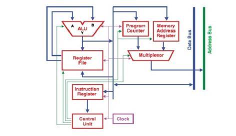
The portion of the central processing unit (CPU) of a computer that controls how the processor operates is called the control unit. It was a component of John von Neumann'sVonNeumannArchitecture.Thecontrolunitis inchargeofinstructingthecomputer'smemory,inputand outputdevices,andarithmetic/logicunitonhowtoreactto commandsgiventotheprocessor.
International Research Journal of Engineering and Technology (IRJET) e-ISSN:2395-0056
Volume: 11 Issue: 05 | May 2024 www.irjet.net p-ISSN:2395-0072
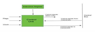
Fig -3:BlockdiagramofRegisterfile
A decoder and a collection of registers make up a basic registerfile.Adatainputandanaddressareneededforthe register function. But in a modern processor architecture, this straightforward register file is useless since there are times when we don't want to write a new value to a register. Additionally, in a single cycle, we usually wish to postbackonevalueandreadtwovaluessimultaneously.
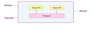
Fig -4:ArithmeticandlogicSignals
3. VERILOG HDL AND XILINX VIVADO
3.1FLOW OF VLSI DESIGN
The formal specification of a VLSI chip is the first step in the VLSI design cycle, which proceeds through several stagestogenerateapackagedchip.
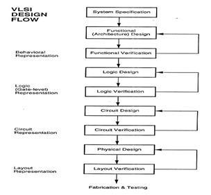
Fig -5:TheflowofVLSIdesign
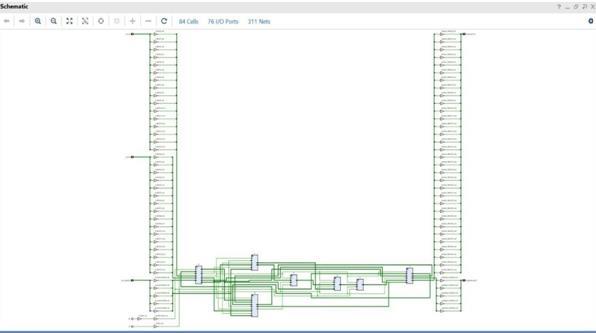
Fig -6:SchematicView
The output of a Vedic multiplier utilizing the UrdhvaTrigbhyam sutra is seen in the following 16-Bit Multiplier simulation result. The MAC procedures are carriedoutusingtwoinputs,a=252andb=846,toproduce anoutputvalueofc=213192.
Compared to other multipliers, the latency and size of the gateriserelativelyslowlyasthenumberofbitsincreases. As a result, the CPU's speed, power, and timing are all efficient.

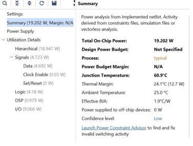
Fig -6: SystemUtilization
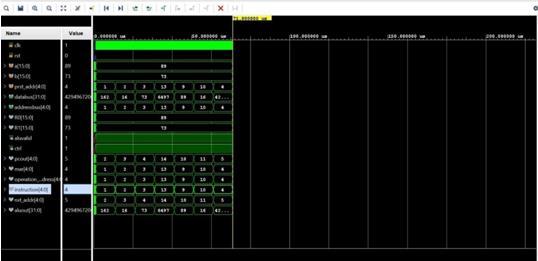
Transcript window results for ALU are displayed in the following figure, which includes all matched conditions. Theprocessormodule'sintegratedmultiplieroperationis executed. The data from the transcript is compared and themultiplicationprocessisconfirmed.
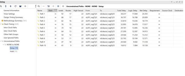
Fig -7:SystemDelay
International Research Journal of Engineering and Technology (IRJET) e-ISSN:2395-0056 Volume: 11 Issue: 05 | May 2024 www.irjet.net p-ISSN:2395-0072
The process of proving a design's functional validity is calledverification.Itistheprocessofmakingthatthelogic designcomplieswiththespecifiedrequirements.
The functioning of the test bench determines verification. The test bench's goal is to ascertain whether the design under test (DUT) is accurate. The Vedic multiplier design is merged with the 16-bit processing module, and the output is confirmed for the specified instruction set. The verification outcomes for the whole processing unit with ALUintegrationareshown.
To build a 16-bit RISC processor, minimum functional units are used. The architecture of Harvard University servedasthemodelfortheplan.TheXilinxVivado2023.1 Design suite tool is used for the design entry and synthesis. According to the synthesis report, the design can achieve a minimum clock period of 14.95 nanoseconds. A simulation tool called Xilinx Vivado 2023.1.Designsuitetoolisemployed.Theaccuracyofthe functionality is assessed by comparing the output of the simulation with the expected results. There are several ways to improve the design. To build a more advanced
design,otherelementsmightbeaddedtothecurrentone. It is possible to increase the amount of instructions the CPUcanprocess.
[1] S. Lad and V. S. Bendre, "Design and Comparison of MultiplierusingVedic Sutras,"20195thInternational Conference On Computing, Communication, Control AndAutomation(ICCUBEA),Pune,India,2019,pp.1-5
[2] Balpande Vishwas V, Abhishek B. Pande, Meeta J. Walke, Bhavna D. Choudhari and Kiran R. Bagade. “Design and Implementation of 16 Bit Processor on FPGA.”(2015).
[3] F.AdamecandT.Fryza,"Design Timeconfigurable processor basic structure," 13th IEEE Symposium on Design and Diagnostics of Electronic Circuits and Systems, Vienna, 2010, pp. 119-120, doi: 10.1109/DDECS.2010.5491804.
[4] Mr. Nishant G. Deshpande, Prof. Rashmi Mahajan, “Ancient Indian Vedic Mathematics based Multiplier Design for High Speed and Low Power Processor”, IJAREEIE,Pune,2014


K.G.VENKATA KRISHNA, Assistant Professor, KrishnaUniversity College of EngineeringandTechnology, KrishnaUniversity, Machilipatnam, A.P,India.
N.K.KAMALA DEVI, StudentofDepartmentof ElectronicsandCommunication Engineering, KrishnaUniversity, Machilipatnam, A.P,India.
K.VISHNU VARMA, StudentofDepartmentof ElectronicsandCommunication Engineering, KrishnaUniversity, Machilipatnam, A.P,India.
International Research Journal of Engineering and Technology (IRJET) e-ISSN:2395-0056
Volume: 11 Issue: 05 | May 2024 www.irjet.net p-ISSN:2395-0072

A.YEDUKONDALU
StudentofDepartmentof ElectronicsandCommunication Engineering, KrishnaUniversity, Machilipatnam, A.P,India.
©2024, IRJET | ImpactFactorvalue:8.226 |