
International Research Journal of Engineering and Technology (IRJET) e-ISSN: 2395-0056
Volume: 11 Issue: 04 | Apr 2024 www.irjet.net
p-ISSN: 2395-0072
International Research Journal of Engineering and Technology (IRJET) e-ISSN: 2395-0056
Volume: 11 Issue: 04 | Apr 2024 www.irjet.net
p-ISSN: 2395-0072
Durga Satish
Jaswanth
12345Graduate Student,6Senior Assistant Professor Department of Electronics and Communication Engineering, Sri Vasavi Engineering College, Tadepalligudem, West Godavari, Andhra Pradesh, India
Abstract –Dual band volumetric antenna using SIW (Substrate Integrated Waveguide) technology is presented in this paper. The volumetric size of the antenna is60 mm× 60 mm× 1.6 mm with rectangular patch and ground plane and fed by a micro strip feed line. A rectangular slot is subtracted from the rectangular patch, design and analyzes the characteristics of the volumetric antenna with varying slot length and width using Ansys HFSS simulation tool. The presented antenna achieves dual bands (VSWR ≤2) 5.7GHz and 5.9GHz with gain of 3.41 dB and 4.96 dB at respective frequencies. The projected antenna is low cost and modeled to be used in Sub-6GHz applications.
Keywords: SIWTechnology,Volumetricantennaand Wirelessmobilecommunication
1. INTRODUCTION
An antenna is the interface between electric currents flowing through metal conductors and radio waves propagating across space. Every radio transmitter and receiver needs to couple their electrical connection to the electromagnetic field.One example of an antenna design with dual functions is the micro strip antenna, which operates in two frequency bands. This is a result of the growing demand to improve the capabilities of wireless systems [1]. The slot patch will, however, modify the emissionpatternsoftheantenna.Switchableslotscanalso be incorporated into the metal patch to create single-feed dual-banddual-polarizedstripantennas[2].
The benefits of substrate integrated waveguide (SIW), including its low cost, low loss, and ease of integration with planar circuits, have been studied [3]–[8]. For integrated microwave and millimeter-wave components and antennas, the SIW has been extensively developed. The dielectric resonator becomes a highly efficient radiator, especially at higher frequencies, when SIW is used to feed it, eliminating the radiation losses of the feeding network [9]. With this method, rows of closely spaced metallic vias between two planes replicate the surrounding walls of a thin rectangular-type waveguide filled with dielectric [10].Many technological challenges arise when using SIW in arrays and antenna structures at lower frequencies. These challenges include reduced dimensions,losses,accurateproductionofSIWstructures,
fabricationconstraints,andsubstrateselection.It appears that the creation of extremely compact and integrated systems is made possible by SIW-based antennas and arrays in wireless systems [11].The Internet of Things (IoT) and Fifth Generation (5G) connectivity have been explored.Among the near-future sub-6GHz applications aresmartgrid,smartcitiesandtelemedicine[12].
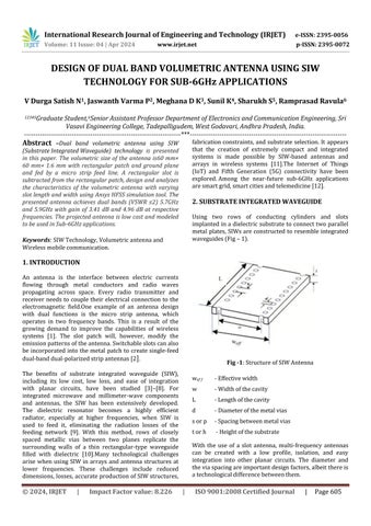
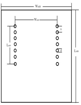
Using two rows of conducting cylinders and slots implantedina dielectricsubstratetoconnecttwoparallel metal plates,SIWsareconstructedto resembleintegrated waveguides(Fig–1).

wef f -Effectivewidth
w -Widthofthecavity
L -Lengthofthecavity
d -Diameterofthemetalvias
sorp -Spacingbetweenmetalvias
torh -Heightofthesubstrate
With the use of a slot antenna, multi-frequency antennas can be created with a low profile, isolation, and easy integration into other planar circuits. The diameter and theviaspacingareimportantdesignfactors,albeitthereis atechnologicaldifferencebetweenthem.
International Research Journal of Engineering and Technology (IRJET) e-ISSN: 2395-0056
Volume: 11 Issue: 04 | Apr 2024 www.irjet.net p-ISSN: 2395-0072
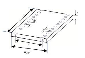
Fig -2:Technologicalgapbetweenthemicrostrippatch andwaveguides
ThepropagationinsideaSIWiscomparabletothatinside atypicalhollowwaveguide,withafewnotableexceptions. The propagating modes resemble the TEn0 mode of the waveguide and are at the TE10 fundamental mode. The size of a SIW and an efficient waveguide with continuous lateralwallsarerelatedbyseveralkeyformulas. It has been discovered that there are empirical correlationsbetweentheSIWdimensionsandtheeffective width(‘weff ’)oftherectangularshapewaveguidewiththe samepropagationparameters.Theserelationshipsemerge from the similarities between the two types of waveguides. Without using full-wave analysis techniques, these connections allow for the early design and dimensioningofSIWcomponents.Amongthecorrelations inthedesignequationsis
The modes of propagation can be deliberate using the empiricalequation(4):
Where ‘d’ is the diameter of the metal vias, ‘w’ signify widthofthecavity,‘weff ’denoteeffectivewidthoftheSIW and‘s’representsspacingbetweenthevias(Fig-1).
(2)
Radiation losses are minimized when the vias' diameters are large enough and their separations from one another aresmallenough.Itispossibletoempiricallyascertainthe viasspacing(s)asafunctionofdiameter(d).
Where L and W are the cavity's length and width, c is the light velocity in free space, and εr is the dielectric substrate's relative permittivity. For the fundamental mode (TE110), m = 1, n = 1 and s = 0. Consequently, SIW designstructuresshowpropagationcharacteristicssimilar torectangularwaveguideswhenthemetalviasareclosely spacedapartandradiationlossesareconsidered.
Antenna
Start
SelectionofSimulationTool

DesignofSIWAntennawithSlot

ResultAnalysisUsing SimulationTool(HFSS)

Comparisonbetween Existing&Proposed AntennaParameters

End

Fig -3:PictorialRepresentationofAntennaDesign
The above flow chart represents the pictorial representationofproposedantenna.
International Research Journal of Engineering and Technology (IRJET) e-ISSN: 2395-0056
Volume: 11 Issue: 04 | Apr 2024 www.irjet.net p-ISSN: 2395-0072
Step 1
Adding the substrate (3D plane)in the Editor window.
Alignthesubstrateusingtheposition.
Assignthedimensionsofthesubstrate.
Step 2
Addingtheground(2Dplane)tothesubstratein theEditorwindow.
Alignthegroundusingtheposition.
Assignthedimensionsoftheground.
Step 3
Addingthepatch(2Dplane)tothesubstratein theEditorwindow.
Alignthepatchusingtheposition.
Assignthedimensionsofthepatch.
Designthespecificshapesbyusinguniteor subtractoptionsinthemenubar.
Step 4
AddPortmaterialtothesubstrate.
Align the material such that it should contain X andZaxisonly.
Assignthedimensionsandposition.
Step 5
Nowaddtheboundariesforthepatchandground.
Rightclickonthepatchineditorwindow>>Goto AssignBoundary>>SelectPerfectE>>Clickok.
Repeatsameforthegroundmaterial.
Step 6
NowaddtheExcitationtotheport.
Rightclick ontheport in editor window>>Goto Assign Excitation>> Select Lumped Port >> Click onNext>>SettheIntegrationlinetoNewLine>> Nowdrawalinefromgroundtopatch.
Step 7
Now go to the project manager and right click on theAnalysis.
Add Solution Setup >> Click on Auto >>Set the Distribution to Linear Step >> Assign the Start, EndandStepSizeFrequency>>ClickOk.
Step 8
Nowfromthemenubargotosimulationoption.
Click on Validate,if all the steps in the validation shows green mark,then go to nextstep otherwise correctthemistakesintheparticularsection.
AftertheValidationstepclickonAnalyseAll.
Step 9
Then will notice some messages in the progress andMessageManagerWindow.
After noticing” Normal completion of simulation onserver:Localmachine”messageinthemessage manager window you can generate the reports from the results section in project manager window.
Step 10
Togeneratetheresults.
Right click on Results >> Create Modal Solution Data Report >> Rectangular Plot >> Select the RequiredParameter>>ClickontheNewReport.
AfterinsertionofInfinitesphere,wecansimulate thegainanddirectivity.
Right click on Results >> Create Far Field Report>>RectangularPlot>>SelecttheRequired Parameter>>ClickontheNewReport.
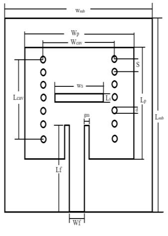
Thisdesign consists ofa ground plane withsubstrateand patchwhichareincommonhavingsomecylindricalholes from top to bottom with some specified measurements called as vias. Vias plays the vital role in the radiation of the signal for an SIW antenna. For obtaining the dual bands introducing a transversal slot in the middle of the antenna(Fig–3)
Width =����/2f�� √(2/����)
���������� =((����+1)/2+(���� 1)/2[1+12ℎ/ ])^(−1/2)
∆�� =0.412∗ℎ((����������+0.3) ( /ℎ+0.264))/((���������� 0.258)( /ℎ+0.8))
Length = ����/(2f��√����������)−2∆��
EffectiveWidth: ������= ��^2/0.95��
Ratioofs/d: ��/��<2.5
ModesofPropagation:
�� 0=��/√(2����)√(( /��)^2+( / )^2+(��/ℎ)^2)
Let ���� =3×10^8 fr = 2.4GHz ���� = 4.4 h = 1.6mm
Width = Vo/2fr √(2/εr) = (3×10^8)/(2×2.4×10^9)√(2/(4.4+1))
Width = 38.036mm
���������� =((����+1)/2+(���� 1)/2[1+12ℎ/ ])^(−1/2) =((4.4+1)/2+(4.4−1)/2[1+12×1.6/16.015])^(−1/2)
International Research Journal of Engineering and Technology (IRJET)
Volume: 11 Issue: 04 | Apr 2024 www.irjet.net
���������� =3.586
∆L =0.412∗ℎ((����������+0.3)
( /ℎ+0.264))/((���������� 0.258)( /ℎ+0.8)) =0.412∗1.6((3.586+0.3)(38.036/1.6+0.264))/ ((3.586−0.258)(38.036/1.6+0.8))
∆�� =0.7528
Length = ����/(2f��√����������)−2∆��
=(3×10^8)/(2×2.4×10^9×√3.586)−2×0.7528 = 31.00436–1.5056
Length = 29.49903mm
Therequiredwidthandlengthofvolumetricantennafor specificParametersare:
Width = 38.036mm
Length = 29.49903mm.
(i) TopView (ii)BottomView
Fig -4:Geometryoftheproposedantenna
Table -1: Dimensionsoftheproposedantenna
SIW Antenna with slot
To obtain the dual band frequency the short transverse slot cut is included into the top plane of the antenna, due tothisslotthefrequencywhichisappliedthroughtheport will be divided in to two frequencies which can be seen through the field distribution pattern. To obtain the most accurateresultsthelengthandwidthofthetransverseslot is varied in steps of 0.2mm and the graphs where plotted for the visual comparison, among all the results the one withslotlengthof1.6mmandwidthof16mmhasproduce thebetterresults.Forboththebandoffrequenciesatthis slotthegainisabove3dBandVSWRisalsointherangeof 1-2andthereturnlosshasabove-16dB
Table -2: ParametricAnalysisbasedonslotdimensions
The presented volumetric antenna with subtracted slot has been simulated and changing slot dimensions with 0.2mm progressive increment using SIW technology by FR4 substrate. Accordingly observe the parameters using simulation tool Ansys HFSS. The simulated antenna top andbottomviewrepresentedintheFig-5
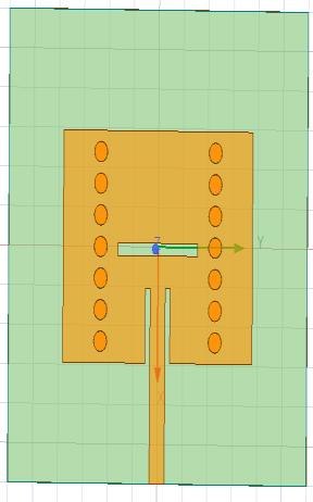
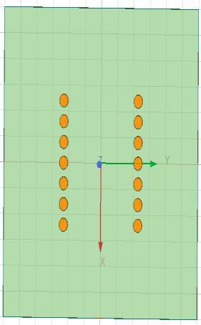
Fig -5:Simulatedantenna
International Research Journal of Engineering and Technology (IRJET) e-ISSN: 2395-0056
Volume: 11 Issue: 04 | Apr 2024 www.irjet.net p-ISSN: 2395-0072
4.1 Return Loss
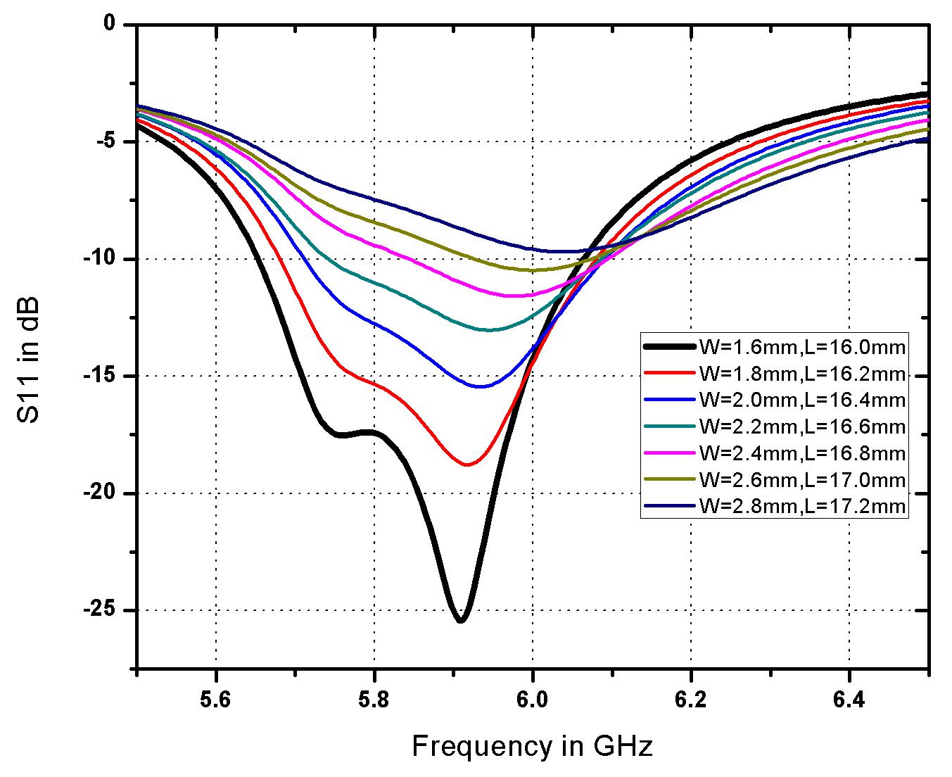
Fig -6:ReturnLoss
By adjusting the slot width and length the results are compared (Table 2) in steps of 0.2mm and plotted and consideringthebestonesrepresentedwithblackcolorfor the return loss obtained dual bands at 5.7GHzand 5.9GHz with-17.3dBand-26.7dBrespectively.
4.2 Voltage Standing Wave Ratio
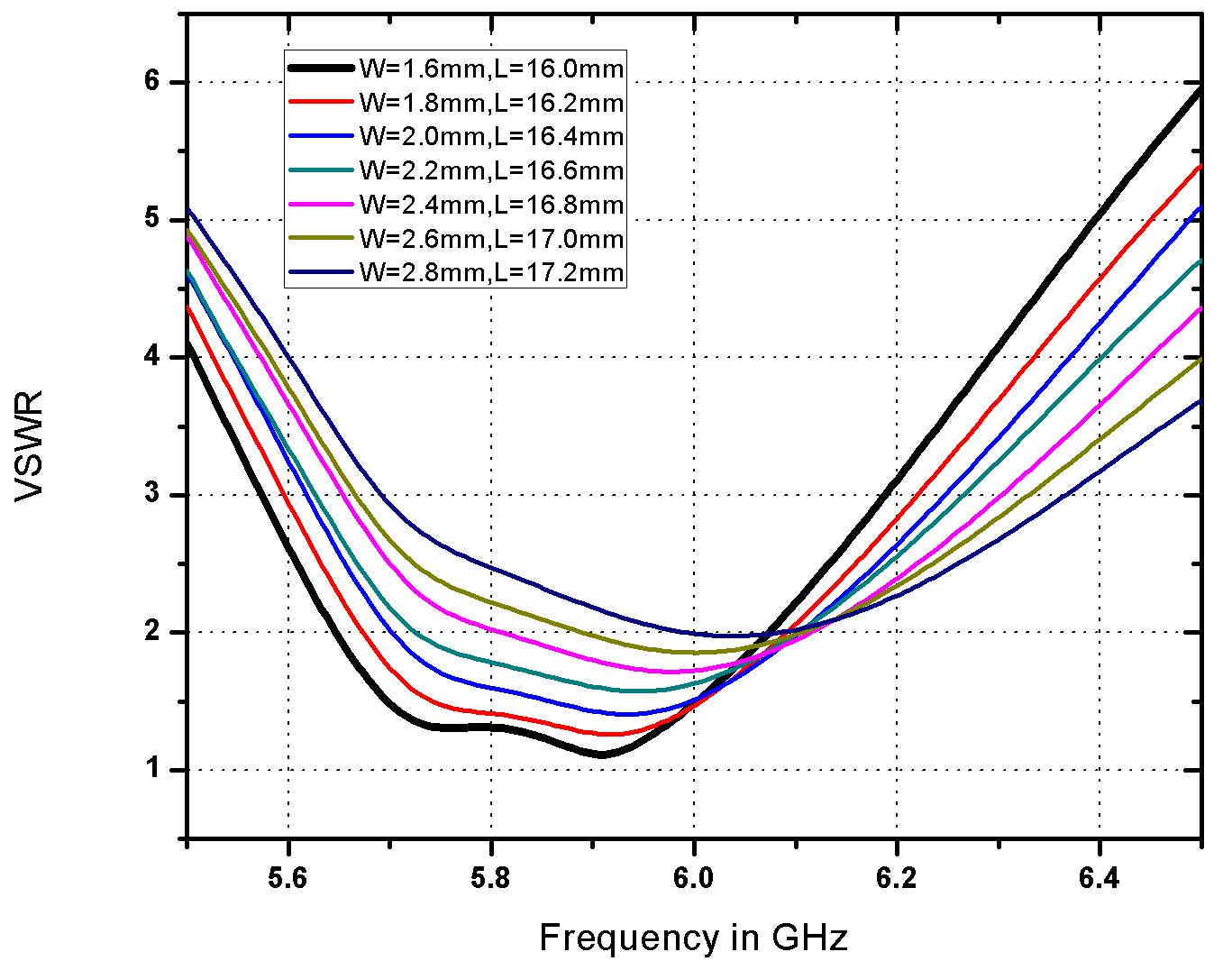
Fig -7:VoltageStandingWaveRatio
TheacceptableVSWRvalueisintherangeof1-2,fromthe VSWR graph plot it is clearly noticed that 1.31 and 1.09 arethevaluesofVSWRatrespectiveradiatingfrequencies.
4.3 Directivity
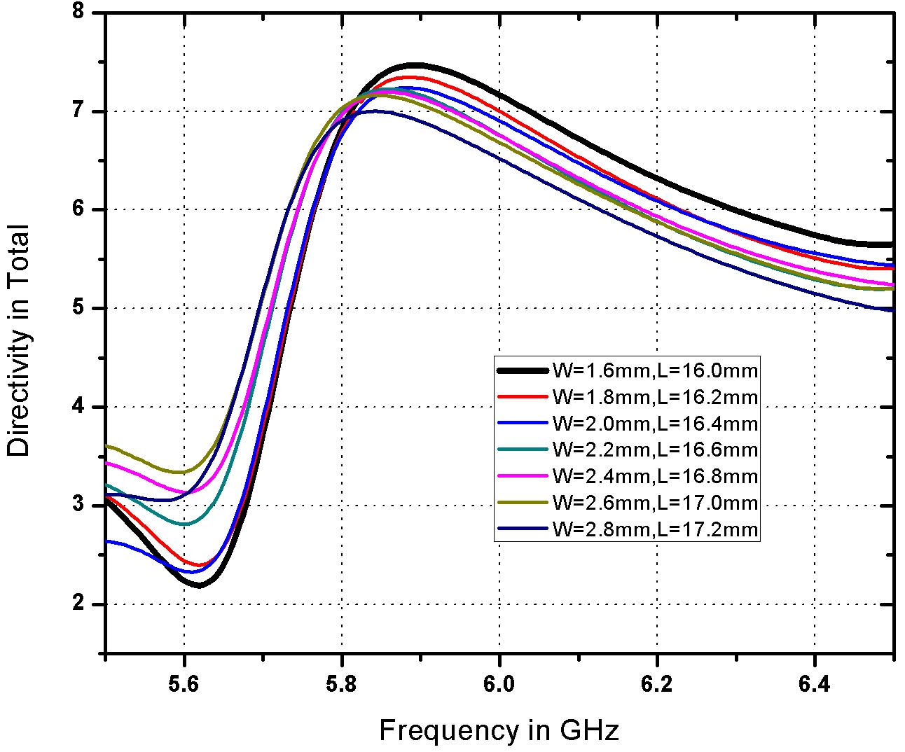
Fig -8:Directivity
Thedirectivityingeneral shouldbemorethanthegain of theantennaandobserveddirectivityofproposedantenna is6.53at5.7GHzand7.47at5.9GHz.
4.4 Gain
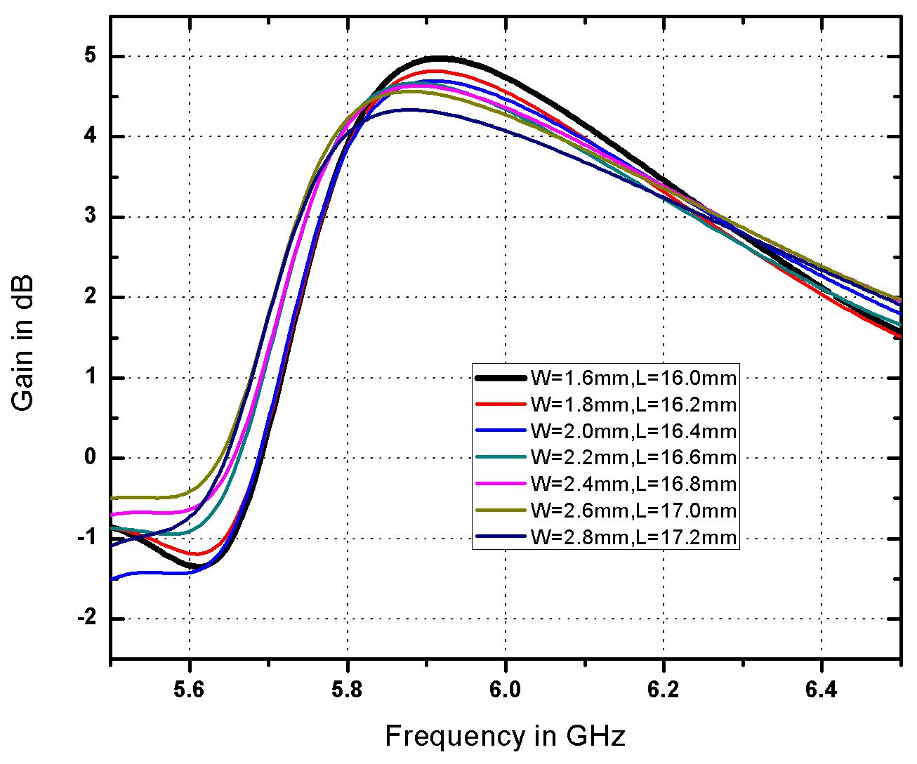
Fig -9:Gain
Theacceptablerangeofgainforanantennaisfromabove 3 dB and for this simulated antenna obtained the gain of 3.41dBat5.7GHzand4.96dBat5.9GHz.
International Research Journal of Engineering and Technology (IRJET) e-ISSN: 2395-0056
Volume: 11 Issue: 04 | Apr 2024 www.irjet.net p-ISSN: 2395-0072
4.5 Bandwidth
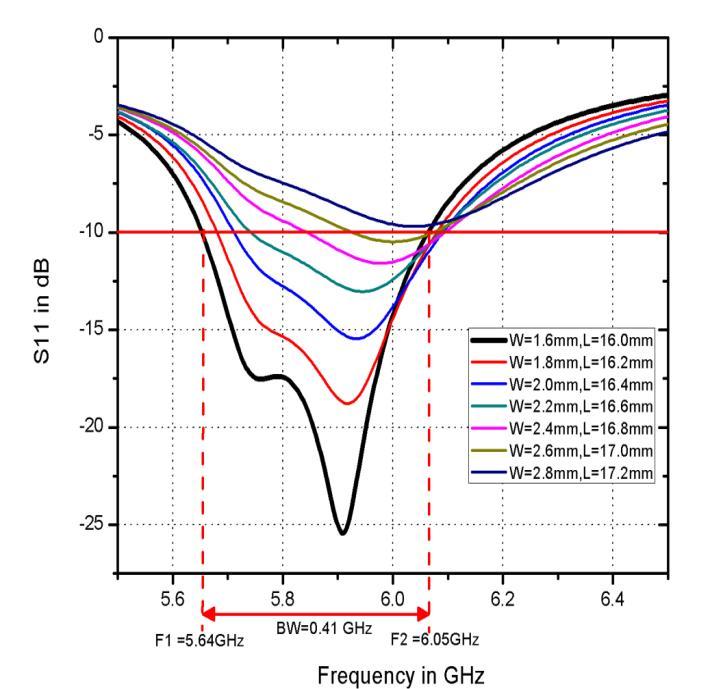
Fig -10:Bandwidth
The bandwidth of an antenna refers to the range of frequencies over which the antenna can operate. The bandwidth for this antenna is about 410MHz which is considerablymorewehaveobtainedtheF1at5.6GHzand F2at6.05GHzandafterthecalculationBW=410MHz[F2–F1].
4.6 E-Field Distribution
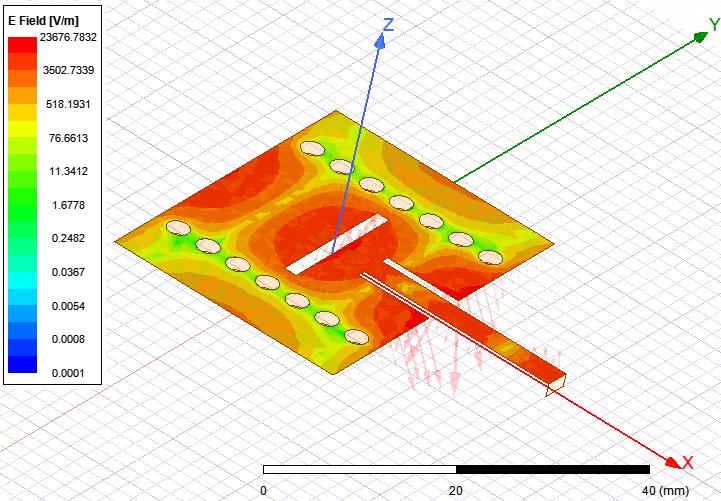
Fig -11:FieldDistribution
TheabovediagramshowstheElectricFieldDistributionof the simulated antenna particularly on patch section, majorityoftheE-Fielddistributioncanbeobservedatslot andedgesofthepatch
4.7 Current Distribution
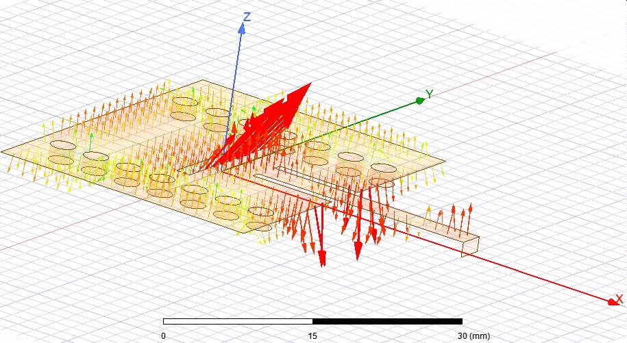
Fig -12:CurrentDistribution
TheCurrentDistributionisalsomaximumaroundtheslot and the edges of the patch and it is low around the vias region.
4.8 Three Dimensional Gain Plots
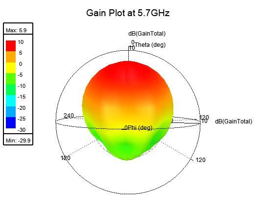
Fig -13:GainPlotat5.7GHz
The above diagram represents 3-dimmensional gain plot whichharvesting5.9dBatradiatingfrequencyof5.7GHz.
International Research Journal of Engineering and Technology (IRJET) e-ISSN:
Volume: 11 Issue: 04 | Apr 2024 www.irjet.net
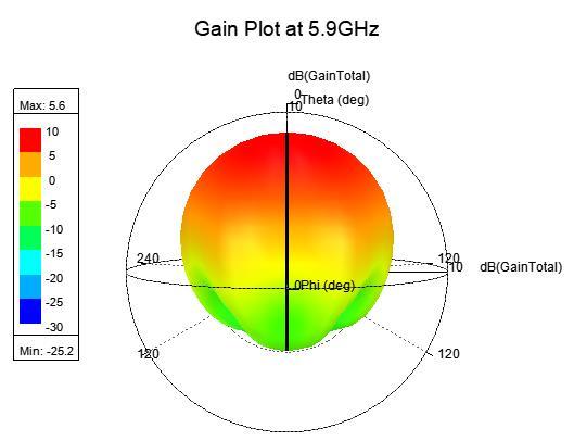
Fig -14:GainPlotat5.9GHz
The Figure-14 shows diagram 3-dimmensional gain plot which produce 5.6dB gain at resonating frequency of 5.9GHz.
4.9 Three Dimensional Directivity Plots
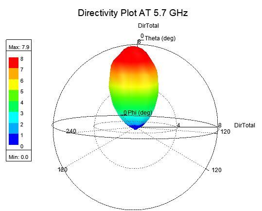
Fig -15:DirectivityPlotat5.7GHz
Theabovediagramshows3-dimmensionaldirectivityplot which obtained directivity of 7.9 at resonating frequency of5.7GHz.
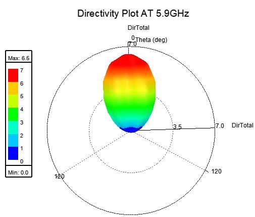
Fig -16:DirectivityPlotat5.9GHz
The Figure-16 represents 3-dimmensionaldirectivity plot which generates directivity of 6.5 at resonating frequency of5.9GHz.
Table -3: Comparisonwithexistingworkswithproposed work
International Research Journal of Engineering and Technology (IRJET) e-ISSN: 2395-0056
Volume: 11 Issue: 04 | Apr 2024 www.irjet.net p-ISSN: 2395-0072
The proposed volumetric antenna with subtracted slot providesbetterresultsascomparedtoreference[13-17]. Significantly gain produced above 3dB at respective resonatingfrequencies5.7GHzand5.9GHz.
Designed the Volumetric Antenna for Dual band frequencies using the SIW Technology and Placed a slot with length of 1.6mm & width of 16mm and obtained the bandsat5.7GHzand5.9GHzwithareturnlossof -17.3dB and -26.7 dB respectively.VSWR of 1.3 at 5.7GHz & 1.0 at 5.9GHz.Gainof3.4dBat5.7GHz&4.9dBat5.9GHz.
Obtainedbandwidthof410MHz(6.05GHz-5.64GHz).This proposed antenna design can be used in Sub-6GHz applications [5G applications] significantly like RF Transceiver, Drone Operations at 5.7GHz and Automatic tollcollection,Spotweather-impactwarnings,Trafficlight controlat5.9GHz(SafetyBand)
This work carried out by Research and Development center, department of ECESriVasaviEngineeringCollege (Autonomous) Tadepalligudem, West Godavari, Andhra PradeshandIndia
[1] Afshinmanesh F, Marandi M and Shahabadi M (2008) Design of a single-feed dual-band dual-polarized printed microstrip antenna using a Boolean particle swarm optimization. IEEE Transactions on Antennas andPropagation56,1845–1852.
[2] N. Jin, F. Yang and Y. Rahmat-Samii, "A Novel Reconfigurable Patch Antenna with Both Frequency and Polarization Diversities for Wireless Communications," IEEE International Symposium on Antennas and Propagation Digest, 2, June 2004, pp. 1796-1799.
[3] D. Deslandes and K. Wu, “Design consideration and performance analysis of substrate integrated waveguide components,” in Proc. 32nd Eur. Microw. Conf.,Milan,Italy,Sep.2002,vol.2,pp.881–884.
[4] Y. Cassivi, L. Perregrini, P. Arcioni, M. Bressan, K. Wu, and G. Conciauro, “Dispersion characteristics of substrate integrated rectangular waveguide” , IEEE Microw. Wireless Compon. Lett., vol. 12, no. 9, pp. 333–335,Sep.2002.
[5] F. Xu and K. Wu, “Numerical multimode calibration technique for extraction of complex propagation constantsofsubstrateintegratedwaveguide,”inProc. IEEE MTT-S Int. Symp., June 2004, vol. 2, pp. 1229–1232.
[6] L.Yan,W.Hong,K.Wu,andT.J.Cui,“Investigationson the propagation characteristics of the substrate integrated waveguide based on the method of lines,” Proc. Inst. Elect. Eng., Microw. Antennas Propag., vol. 152,pp.35–42,Feb.2005.
[7] F. Xu and K. Wu, “Guided-wave and leakage characteristics of substrate integrated waveguide,” IEEE Trans. Microw. Theory Tech., vol. 53, no. 1, pp. 66–73,Jan.2005.
[8] D. Deslandes and K. Wu, “Accurate modeling, wave mechanisms,anddesignconsiderationsofasubstrate integrated waveguide,” IEEE Trans. Microw. Theory Tech.,vol.54,no.6,pp.2516–2526,Jun.2006.
[9] Abhishek Sharma, Anirban Sarkar, Animesh Biswas and M. Jaleel Akhtar “Substrate integrated waveguide fed dual-frequency dual-linearly-polarized dielectric resonator antenna,”International Journal of Microwave and Wireless Technologies,Volume 10,Issue4,May2018,pp.505–511
[10] D.Deslandes, and K. Wu “Design consideration and performance analysis of substrate integrated waveguide components,” 32nd European Microwave Conference(EuMC2002),Milan,Italy,pp.1-4.
[11] Kordiboroujeni Z and Bornemann J (2013) Designing the width of substrate integrated waveguide structure. IEEE Microwave and Wireless Components Letters23,518–520.
[12] K. M. Mak, H. W. Lai and K. M. Luk, "A 5G Wideband Patch Antenna with Antisymmetric L-shaped Probe Feeds," IEEE Trans. Ant. Propag., vol. 66, no. 2, pp. 957-961,2018.
[13] X. Zhu, X. Liu, and H. Yang, ‘‘Compact dual-band wearable textile antenna based on quarter-mode substrate integrated waveguide,’’ in Proc. 9th Asia–Pacific Conf. Antennas Propag. (APCAP), Xiamen, China,pp.1–2,Aug.2020
[14] Caytan O et.al, “Half mode substrate-integratedwaveguide cavity-backed slot antenna on cork substrate”, IEEE Antenna Wireless Propagation Letters,vol.15,pp.162-165,February2016.
[15] SenYanet.al,“Dual-BandTextileMIMOAntennaBased on Substrate-Integrated Waveguide (SIW) Technology”, IEEE Transactions on Antennas and PropagationVolume:63,Issue:11,November2015.
[16] Taiwei Yue and Douglas H. Werner,“A Compact DualBand Antenna Based on SIW Technology”IEEE International Symposium on Antennas and Propagation & USNC/URSI National Radio Science Meeting,2018
International Research Journal of Engineering and Technology (IRJET) e-ISSN: 2395-0056
Volume: 11 Issue: 04 | Apr 2024 www.irjet.net p-ISSN: 2395-0072
[17] Choudhury,S.,Mohan,A.,&Guha,D.SIW-induceddual modedualband loop antenna: A new design insight and guideline. Microwave and Optical Technology Letters,60(1),50–56,2017.


Mr. V Durga Satish N Final Year
B.Tech student in the Electronics & CommunicationEngineering DepartmentatSriVasaviEngineering College(A),Tadepalligudem, WestGodavari,Andhra Pradesh and India
Mr. Jaswanth Varma P Final Year
B.Tech student in the Electronics & CommunicationEngineering DepartmentatSriVasavi EngineeringCollege(A) Tadepalligudem,WestGodavari, AndhraPradeshandIndia.
Ms. Meghana D K FinalYear
B.Tech student in the Electronics & CommunicationEngineering DepartmentatSriVasavi EngineeringCollege(A) Tadepalligudem,WestGodavari, AndhraPradeshandIndia.
Mr. Sunil K Final Year B.Tech studentintheElectronics& CommunicationEngineering DepartmentatSriVasavi EngineeringCollege(A) Tadepalligudem,WestGodavari, AndhraPradeshandIndia.
Mr. Sharukh S Final Year B.Tech studentintheElectronics& CommunicationEngineering DepartmentatSriVasavi EngineeringCollege(A) Tadepalligudem,WestGodavari, AndhraPradeshandIndia.
Ramprasad Ravula Completed his M.Techin2009fromJNTUK,Kakinada, Andhra Pradesh. He has totally 15 Yearsofteachingexperience.Presently heisworkingasSr.AssistantProfessor in the Department of Electronics and Communication Engineering of Sri Vasavi Engineering College (A), Tadepalligudem, West Godavari, Andhra Pradesh and India. His interested areas of Research are AntennassignificantlySIWantenna.