
International Research Journal of Engineering and Technology (IRJET) e-ISSN:2395-0056
Volume: 11 Issue: 04 | Apr 2024 www.irjet.net
p-ISSN:2395-0072
International Research Journal of Engineering and Technology (IRJET) e-ISSN:2395-0056
Volume: 11 Issue: 04 | Apr 2024 www.irjet.net
p-ISSN:2395-0072
Santhosh Kumar D1 , Preethi A2, Shobana S3
Assistant professor, Department of EEE ,Vivekanandha College of Engineering forWomen, TamilNadu
Assistant Professor,Department of EEE,Vivekanandha College of Engineering forWomen, TamilNadu
Research Scholar, Department of EEE ,Vivekanandha College of Engineering forWomen, TamilNadu
Abstract
A Multilevel inverter is a force electronic gadget that is utilized for high voltage and high force applications and has numerousfavourablecircumstanceslike,lowexchangingpressure,lowabsoluteconsonanttwisting(THD).Thus,thesize and cumbersomeness of detached channels can be diminished. This work proposes another geography of a 7-level fell staggeredinverterwithdecreasednumberofswitchesthanthatoftraditionalsortwhichhas12switches.Thegeographies compriseofcircuitwith7switchesforasimilar7-levelyield.Hencewithlessnumberofswitches,therewillbeadecrease in door drive hardware and furthermore not many switches will lead for explicit timespans. The SPWM procedure is executed utilizing multicarrier wave signals. The circuit is displayed and recreated with the assistance of MATLAB/SIMULINK.
Keywords: Cascaded Multilevel Inverter(CMLI), Diode Clamped Multilevel Inverter(DCMLI), Flying Capacitor, Pulse Width Modulation (PWM), Selective Harmonic Elimination
1
As of late, the requirement for high force mechanical assembly has been determined by various modern applications. Medium voltage engine drives and utility applications are a few models, since they require medium voltage andmegawattpowerlevel.Anotherapplicationrespectsmediumvoltagematrices,whereitisproblematictointerfacejust one force semiconductor switch straightforwardly. Therefore, a few staggered power converter structures have been presented as an option in high force and medium voltage applications. Staggered converters accomplish high force appraisals,yetadditionallyempowertheutilizationofenvironmentallyfriendlypowersources.Thispartexaminesabout thekindsofstaggeredinvertersanditspreferences.
Multilevel converters not just create the yield voltages with low bending, yet in addition lessen the dv/dt stresses, henceforth electromagnetic compatibility (EMC) issues can be diminished. In addition, three diverse major staggered converterdesigns,forexample,fellH-spansconverterwithisolateddcsources,diodeclipped(nonpartisanclasped)and flyingcapacitors(capacitorbraced)havebeenaccountedforinthewriting.
1.1.1
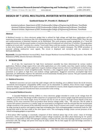
A Cascaded Multilevel Inverter (CMLI) is a force electronic gadget intended to create an AC voltage from DC voltagesofafewlevels.ThisdesignofCMLIcomprisesofaprogressionofH-connect(single-stagefullextension)inverter units in every one of its three stages. Every H-connect unit has its own dc source. Through various blends of the four switches, S1-S4, every converter level can produce three diverse voltage yields, +Vdc, - Vdc and zero. The AC yields of variousfull-connectconvertersinasimilarstageareassociatedinarrangementwiththeendgoalthattheincorporated voltagewaveformistheamountoftheindividualconverteryields.EveryH-connectunitcreatesasemisquarewaveform bystagemovingitspositiveandnegativestagelegsexchangingtime.Eachexchanginggadgetconsistentlyleadsfor180° paying little heed to the beat width of the semi square wave. This exchanging strategy causes current pressure of the wholeexchanginggadgetsasequivalent.
A three-phase CMLI topology is essentially composed of three identical phase legs of the series- chain of H-bridge converters, which can possibly generate different output voltage waveforms and offers phase-balancing for AC system. ThisfeatureisimpossibleinotherVSItopologiesutilizingacommonDClink.Sincethistopologyconsistsofseriespower conversion cells, the voltage and power level may be easily scaled. The dc link supply for each full bridge converter is providedseparately.
International Research Journal of Engineering and Technology (IRJET) e-ISSN:2395-0056
Volume: 11 Issue: 04 | Apr 2024 www.irjet.net
p-ISSN:2395-0072
Asingle-phasestructureofanm-levelcascadedinverterisillustratedinFigure1.1. Eachseparatedcsourceisconnected toasingle-phasefull-bridge,orH-bridge,inverter.Eachinverterlevelcangeneratethreedifferentvoltageoutputs,+Vdc,0 and–Vdcbyconnectingthedcsourcetothedifferentcombinationsofthefourswitches,S1,S2,S3andS4.Toobtain+Vdc, switchesS1andS4areturnedon,whereas –VdccanbeobtainedbyturningonswitchesS2andS3.ByturningonS1and S2orS3andS4,theoutputvoltageiszero.
Theacoutputsofeachofthedifferentfull-bridgeinverterlevelsareconnectedinseriessuchthatthesynthesizedvoltage waveformisthesumoftheinverteroutputs.
Thephasevoltagewaveformforan5-levelcascadedH-bridgeinverterwith2separatedcsourcevoltageand2fullbridges isshowninFigure1.2
Thustheoutputvoltageofaphaseisgivenas Van=Va1+Va
Thus,thepredominantlowerfrequencyharmonicssuchas5th,7th ,11th and13th harmonicsareeliminatedwhileusingthis configuration.
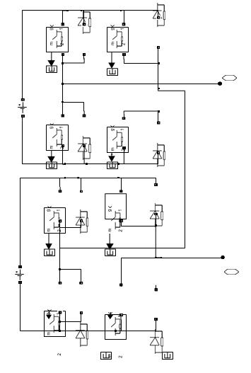
Figure1Topologyofacascadedmultilevelinverterinonephase
International Research Journal of Engineering and Technology (IRJET) e-ISSN:2395-0056
Volume: 11 Issue: 04 | Apr 2024 www.irjet.net
Figure2TheoutputvoltagewaveformofH-bridge
p-ISSN:2395-0072
Multilevel cascaded inverters have been proposed for the applications such as static var generation, an interface with renewable energy sources and for battery-based applications. Cascaded inverters are also proposed for use as the main tractiondriveinelectricvehicles.Besidethis,theapplicationsofthecascadedinvertersareasfollows:
1.Itismoresuitableforhigh-voltage,high-powerapplicationsthantheconventionalinverters.
2. It generates a staircase voltage waveform approaching a sinusoidal output voltage thereby increasing the number of levels.Itdoesnotrequireanyvoltagebalancecircuitsorvoltagematchingdevicesasitconsistsofacascadedconnection ofmanysingle-phase,fullbridgeinverterfedwithaseparateDCsource.
The general structure of the multilevel inverter is to synthesize a sinusoidal voltage from several levels ofvoltages typically obtained from capacitor voltage sources. A three level inverter, also known as a “neutral-clamped” inverter, consists of two capacitor voltages in series and uses the center tap as the neutral. Each phase leg of the three-level inverter has two pairs of switching devices in series. The center of each device pair is clamped to the neutral through clampingdiodes.Theoutputobtainedfromathree-levelinverterisaquasi-squarewaveoutputiffundamentalfrequency switching is used. Multilevel inverters are being considered for an increasing number of applications due to their high powercapabilityassociatedwithloweroutputharmonicsandlowercommutationlosses.
Multilevelinvertershavebecomeaneffectiveandpracticalsolutionforincreasingpowerandreducingharmonicsof AC load. The main multilevel topologies are classified into three categories: diode clamped inverters, flying capacitor inverters,andcascadedinverters.Inathree-phaseinvertersystem,thenumberofmainswitchesofeachtopologyisequal. Comparingwiththenumber ofothercomponents,forexample, clampingdiodesand dc-link capacitorshavingthesame capacity per unit, diode clamped inverters have the least number of capacitors among the three types but require additional clamping diodes. Flying capacitor inverters need the most number of capacitors. But cascaded inverters are considered as having the simplest structure. The diode clamped inverter, particularly the three-level one, has drawn much interest in motor drive applications because it needs only one common voltage source. Also, simple and efficient PWM algorithms have been developed for it, even if it has inherent unbalanced dc-link capacitor voltage problem. However,itwouldbea limitationtoapplicationsbeyondfour-level diodeclampedinvertersfor thereasonofreliability andcomplexity considering dc-link balancingandthe prohibitivelyhighnumberofclampingdiodes.MultilevelPWMhas lowerdv/dtthanthatexperienced in some two-level PWM drives because switching is between several smaller voltage levels.Diodeclampedmultilevelinverterisaverygeneralandwidelyusedtopology.DCMLIworksontheconceptofusing diodestolimitvoltagestressonpowerdevices.ADCMLItypicallyconsistsof(m-1)capacitorsontheDCbuswheremis thetotalnumberofpositive,negativeandzerolevelsintheoutputvoltage.ThephaseaoutputvoltageVanhasfivestates: Vdc/2,Vdc/4,0,-Vdc/4and-Vdc/2.
International Research Journal of Engineering and Technology (IRJET) e-ISSN:2395-0056
Volume: 11 Issue: 04 | Apr 2024 www.irjet.net p-ISSN:2395-0072
1.1.3
Another fundamental multilevel topology, the flying capacitor, involves series connection of capacitor clamped switchingcells.Thistopologyhasseveral uniqueandattractivefeatureswhencomparedtothediode-clampedinverter. One feature is that added clamping diodes are not needed. Furthermore, the flying capacitor inverter has switching redundancywithinthephasewhichcanbeusedtobalancetheflyingcapacitorssothatonlyonedcsourceisneeded.
Figure4showsthethree-levelflyingcapacitorinverter.Thegeneralconceptofoperationisthateachflyingcapacitoris chargedtoone-halfofthedcvoltageandcanbeconnectedinserieswiththephasetoaddorsubtractthisvoltage.
1.2
Aschemeforfinitestatemodelpredictivecontrol-fedfive-levelcascadedMLIhasbeenestablished.Thisproposed method uses 19 voltage vectors out of totally 125 voltage vectors of the cascaded MLI. Since this inverter has many switchesandreducestheaverageswitchingfrequencywhichisamatterofgreatimportanceforhighvoltageapplications, as they contribute to significant switching losses. Two schemes of Finite State Model Predictive Control (FSMPC) are proposedi.e.FSMPC-1employingthecurrentcontrolofthecascadedMLIwith19voltagevectorsandFSMPC-2aimingthe controlofinverterloadcurrentaswellasreducingtheaverageswitchingfrequencyusing19vectors.Theperformanceof the proposed schemes is compared with a conventional 61 voltage vector scheme of the cascaded inverter. The results
International Research Journal of Engineering and Technology (IRJET) e-ISSN:2395-0056
Volume: 11 Issue: 04 | Apr 2024 www.irjet.net p-ISSN:2395-0072
showthatboththeproposedschemesperformwellforsteadystateanddynamicoperatingconditions(RaziaSultanaetal. 2016).
Anovelspace-vectorcurrent-controlstrategyhasbeenemployedtomaintainthedesirednumberofvoltagelevelsbased on load current, in a newer five-level single-phase voltage source inverter. With the proper selection of the redundant inverterswitchingstates,thedeviationinneutral-pointvoltageisconsiderablyminimized(AmmarMasaoudetal.2014). Tobalanceconductionlossesinfull-bridgeandMulti-LevelCascadeInverters,aswitchingmethodhasbeenproposed,and itseffectivenessandvalidityhavebeenexamined(HosseiniAghdametal.2008).
In 1999, Tolbert & Habetler found that the implementation of the existing control strategies for a DC-MLI impingesontheswitchutilization,thusincreasingthelosses.In2000,Mcgrath& Holmesobtainedananalytical solution forPWMtechniquesandfoundthattheharmoniccomponentsproducedbyAPODtechniqueinDC-MLIsproducethesame effectasthatofthePSCinCHBMLIs.In2001,Calaisetal.reviewedtheMCPWMmethods.Afewregularsampledcontrol strategies apposite for MLIs are also available based on either solving complex equations or evolutionary computing. A general Space Vector PWM (SVPWM) method for MLI based on a generalization of dwell-times calculation has been achieved(Trabelsietal.2012).
The presented scheme is developed for CHBMLI in which the sectors are defined by two parameters serving for easy calculationofdwell-times.ThispaperintroducedanewswitchingschemeforanewtopologyofMLIwithreducednumber of switches for interfacing fuel-cell with the grid. An unipolar PWM technique has been coined for the switching of MLI topologywithreducednumberofswitchesforinterfacingfuel-cellwiththegrid(Kumar&Pal2014).AlevelshiftedPWM controlstringsource-basedMLItopologyhasbeenformulated.ThistopologyworkswiththeinnovativePWMstrategyin achieving the targeted output. In this case, the DC source is connected with controlled switch by level shifted PWM technique, which is connected across an anti-parallel diode and such types of controlled sources are placed in series (Subbaraoetal.2014).
The Third Harmonic Injection PWM (THIPWM) strategy of a seven-level Uniform Step Cascaded H-Bridge Asymmetrical Inverter(USCHBAI)hasbeendetailedwiththecomparisonofSPWMstrategy(Talebetal.2015).
A single-phase modified H-Bridge seven-level inverter structure has been schemed suitable for stand-alone PV systems. Selective Harmonic Elimination (SHE) technique involving Newton-Raphson method has been used to solve the non-linearequationsfromtheswitchingangles(Krismadinataetal.2013).ABacterialForagingAlgorithm(BFA)method is proposed for switching angle selection in PWM inverter. The problem of voltage harmonic elimination together with output voltage regulation is drafted as an optimization task and the solution is sought through the proposed method. Extensive simulations are carried out using MATLAB/SIMULINK environment under various operating points with different switching pulses per half cycle. To demonstrate the superiority of the proposed method, BFA results are comparedwithotherexistingtechniquessuchasGeneticAlgorithm(GA)andParticleSwarmOptimization(PSO)method (SudhakarBabuetal.2015).
A generalized Hybrid single-carrier sinusoidal modulation control for cascaded MLIs has been devised. This scheme combines the features of single-carrier sinusoidal and fundamental frequency modulations. The important characteristic ofthismodulationisbetterharmonicperformanceandreducedswitchinglosses(Govindaraju&Baskaran2011).
Mainlythepowerelectronicconvertersareoperatedin the“switchedmode”state.Thus,theswitcheswithinthe converterarealwaysineitheroneofthetwostates-turnedofforturnedoncondition.Tocontroltheflowofpowerinthe converter,theswitchesalternatebetweenthesetwostates(i.e.onandoff).Thishappensrapidlysothattheinductorsand capacitors at the input and output averages or filters the switched signal. This process is called Pulse Width Modulation (PWM),sincethedesiredaveragevalueiscontrolledbymodulatingthewidthofthepulses.
Formaximumattenuationoftheswitchingcomponent,theswitchfrequency fcshouldbehigherthanthefrequencyofthe desiredfundamentalACcomponent.
ThisPWMcanberealizedusingdifferenttechniquessuchascarrierbasedPWM,PWMwithharmonicsminimizationand spacevectorPWM.ThecarrierPWMcanbenaturalPWM,symmetricPWMandasymmetricPWM.
The most simple and well known PWM technique is the sinusoidal PWM. This technique uses a controller which determines the voltage reference of the inverter from the error between the measured current and its reference. This
International Research Journal of Engineering and Technology (IRJET) e-ISSN:2395-0056
Volume: 11 Issue: 04 | Apr 2024 www.irjet.net
reference voltage is then compared with a triangular carrier signal. The output of this comparison decides the switching functionoftheVSI.Thechoiceoftheratiobetweenthefrequencyofthereferencesignalandthefrequencyofthecarrier signal is very important in the case of symmetric and periodic reference. As a consequence, in the case of sinusoidal reference, the ratio between the two frequencies must be integer to synchronize the carrier with the reference. It is preferablethatthecarrierfrequencybeoddtoconservethereferencesymmetry.In allcasesthisratiomustbesufficiently high to ensure the fast switching and to take the switching harmonics away from the fundamental produced by the inverter.
In this technique, the switching angles are computed offline and are calculated in such a way that arbitrary harmonics,usuallyloworder,upto (a-1) harmonics are eliminated, where “a” is the number of switching angles. Theswitchinganglesmustbelowerthan90°.Iftheanglesarelargerthan 90°thantheactualoutputsignalwouldnotbe achieved.Higherorderharmonicscanbefilteredusingadditionalfiltersbetweentheinverterandtheload.
This modulation operates at a very low switching frequency to reduce the semiconductor losses. To minimize harmonic distortion low frequency harmonics are chosen for elimination by properly selecting angles among different levelinverters.
Each multilevel inverter has several switching states which generate different voltage vectors and can be used to modulatethereference.Thereferencesignalisgeneratedfromitsclosestsignals.SVMidentifieseachswitchingstateofa multilevelinverterasapointincomplexspace.Thenreferencephasorrotatinginthe planeatthefundamentalfrequency is sampled within each switching period and the nearest three inverter switched states are selected with duty cycles calculated to achieve the same volt-second average as the sampled reference phasor. This directly controls the inverter line to line voltages and only implicitly develops the phase leg voltages (Massoud et al 2007a, Massoud et al 2007b, Massoudetal2008).
PrincipleofSpaceVectorPWM
a. Treatsthesinusoidalvoltageasaconstantamplitudevectorrotatingatconstantfrequency
b. ThisPWMtechniqueapproximatesthereferencevoltageVrefbyacombinationoftheeightswitchingpatterns(V0to V7)
c. Coordinate Transformation (abc reference frame to the stationary d-q frame): A three-phase voltage vector is transformedintoavectorinthestationaryd-qcoordinateframewhichrepresentsthespatialvectorsumofthethreephasevoltage
d. Thevectors(V1toV6)dividetheplaneintosixsectors(eachsector:60degrees)
e. Vrefisgeneratedbytwoadjacentnon-zerovectorsandtwozerovectors
The carrier frequency is the same as the switching frequency. If the modulation were reduced to zero or a DC quantity,thenthePWMspectrumwouldconsistofthecarrieranditsharmonicsalone.Astheamplitudeofthemodulating waveformisincreased,sidebandsappearandincreaseinamplitudeoneithersideofthecarrieranditsharmonics.Asthe frequencyofthemodulatingwaveformisincreased,thesidebandsspreadawayfromthecentralcarrierfrequency.
The carrier frequency should be synchronous, that is an integer multiple of the fundamental frequency, if the pulse numberislow(sayN<21).Anoddmultipleguaranteeshalfandquarterwavesymmetryandthereforenoevenharmonics occurinthecarrierspectrum.
IfthesamecarriersignalisusedtogenerateallthreephaselegPWMsignalsinathreephaseinverter,thecarrier spectraltermsinthephaselegsignalswillalsobeidentical.Thusthecarrierspectralterms(butnotthecarriersidebands or modulating terms) will be cancelled in the phase to phase waveforms. This is true regardless of the pulse number N. Although thephaserelationshipbetweenthemodulatingandcarrierwaveformscanbearbitrary,itissuggestedthatthe slopesofthetriangularcarrierandmodulatingwaveform,ifsinusoidalincharacter,shouldbeoftheoppositepolarityat the coincident zero crossings, especially for low N. This has practical implementation advantages of preserving the
11
04 | Apr 2024 www.irjet.net p-ISSN:2395-0072
accuracy of the edges in analog implementations and easing the transition between different pulse numbers in systems where this may change during operation. Additionally this 180 degree phase difference (phase relative to the carrier period)resultsintheminimizationoftheharmoniclossesinaninductiveload.This180degreeout-of-phaserelationship canonlyexistforoddN.Further,thereductioninharmoniclossesduetoaspecificphaserelationshipbetweenmodulating functionandcarrierisonlysignificantforoddN.Toachievethisphaserelationshipinathreephaseinverterforallthree phasesrequiresNtobeanoddmultipleofthree(N=3,9,15,21...),ifthesamecarrieristobeusedforallthreephasesto achievecarriercancellationinthephase-phaseoutput.
In a multi-level converter with an integer pulse number, only one carrier can ever meet this requirement, as the other carriersareusuallyphaseshiftedrelativetoit.However,ifanon-integersynchronouspulsenumberisusedinamultilevel converter,thisphaserelationshiponceagainbecomesvalid.
(i)Carrier Switching Frequency Sub Harmonic Pulse Width Modulation (CSFSHPWM)
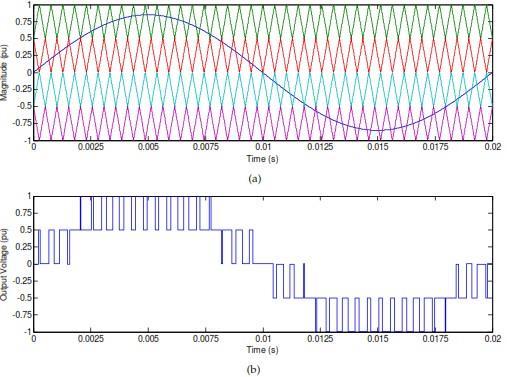
For an m-level inverter, this technique uses (m-1) triangular carrier signals with the same frequency (fc), same peak-topeak amplitude(Ac)andsamephasewhicharedisposedsuchthatthebandstheyoccupyarecontiguous.Thesinusoidal modulation waveform is centered in the middle of the carrier set and is continuously compared with each of the carrier signals.Ifthereferenceisgreaterthanacarriersignal,thentheactivedevicecorrespondingtothatcarrierisswitchedon andif the reference isless thana carriersignal,then theactivedevicecorrespondingtothat carrier isswitchedoff.This method is also known as sinusoidal pulse width modulation (SPWM). In multilevel inverters, the amplitude modulation indexmaandthefrequencyratiomfaredefinedasgivenas
ma=Am/(m−1).Ac (3.1)
mf=fc/fm (3.2)
TheCSFSHPWMcontrolmethodalongwithcarrierandmodulatingwaveformsareshowninFigure5
Anothercarrierbasedmethodformultilevelapplicationsistermedasswitchingfrequency optimalPWM(SFO-PWM) and it is similar to SH-PWM except that a zero sequence (triplen harmonic) voltage is added to each of the carrier waveforms. This method takes the instantaneous average of the maximum and minimum of the three reference voltages (Va∗ , Vb∗ and Vc∗) and subtracts this value from each of the individual reference voltages to obtain the modulation waveforms.TheCSF-O-PWMcontrolmethodalongwithcarrierandmodulatingwaveformsareshowninFigure.
International Research Journal of Engineering and Technology (IRJET) e-ISSN:2395-0056 Volume: 11 Issue: 04 | Apr 2024 www.irjet.net p-ISSN:2395-0072
(iii) Variable Switching Frequency Multi-Carrier Sub Harmonic Pulse Width Modulation (VSFMC-SH-PWM)
In this technique for a multi-level inverter, (m-1) carrier signals with different switching frequencies are used withsinusoidalreferencesignals.
(iv) Variable Switching Frequency Multicarrier Optimal Pulse Width Modulation (VSFMC-O-PWM)
For a multilevel inverter, if the levels are ‘m’ there will be ‘(m-1)’ carrier set with variable switching frequency multi carrierpulsewidthmodulation.
(v) Carrier Phase Shifted Sub Harmonic PWM (CPS-SHPWM)
In the phase shifted multicarrier modulation, all triangular carriers have same frequency and the same peak to peak amplitudebutthereisaphaseshiftbetweenanytwoadjacentcarrierwaves.Gatesignalsaregeneratedbycomparingthe modulatingwavewiththecarrierwaves.InthisPWMmethodtheequivalentswitchingfrequencyofthewholeconverter is (m-1) times the switching frequency of each power device. This means CPS-PWM can achieve a high equivalent switchingfrequencyeffectatverylowrealdeviceswitchingfrequencywhichismostusefulinhighpowerapplications.
(vi) Alternate Phase Opposition Disposition (APOD) PWM
In this modulation, alternative carrier waves are phase displaced by 180°. The APOD-PWM control method along with carrierandmodulatingwaveformsareshowninFigur.TherulesforAPODmethod,
i) Theconverterswitchesto+Vdc/2whenthereferenceisgreaterthanallthecarrierwaveforms.
ii) The converter switches to Vdc / 4 when the reference is less than the uppermost carrier waveform and greaterthanallothercarriers.
iii) Theconverterswitchesto0whenthereferenceislessthanthetwouppermostcarrierwaveformandgreater thantwolowermostcarriers.
iv) Theconverterswitchesto - Vdc/4whenthe reference isgreaterthanthelowermostcarrier waveformand lesserthanallothercarriers.
v) Theconverterswitchesto-Vdc/2whenthereferenceislesserthanallthecarrierwaveforms.
International Research Journal of Engineering and Technology (IRJET) e-ISSN:2395-0056
Volume: 11 Issue: 04 | Apr 2024 www.irjet.net
p-ISSN:2395-0072
Figure7APOD-PWMtechnique:a)Referenceandcarriersignals,b)Outputphasevoltagewaveform (vii) Phase Opposition Disposition PWM (POD-PWM)
In POD-PWM control technique, the carrier signals which are above the zero level are in phase and the carrier signalswhicharebelowthezerolevelareinphaseofeachotherandoutofphaseby180°toabovesignalswhichisshown inFigure3.4.
Therulesforthephaseoppositiondispositionmethodforamultilevelinverterare
i) Theconverterisswitchedto+Vdc/2whenthereferenceisgreaterthanbothuppercarrierwaveforms.
ii) Theconverterisswitchedtozerowhenthereferenceisgreaterthanthelowercarrierwaveformbutlessthan theuppercarrierwaveform.
iii) Theconverterisswitchedto-Vdc/2whenthereferenceislessthanbothcarrierwaveforms.
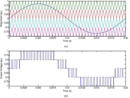
Figure7POD-PWMtechnique:a)Referenceandcarriersignals,b)Outputphasevoltagewaveform (viii) Phase Disposition PWM (PD-PWM)
InPD-PWMmodulation,allthecarriersignalsareinphase.Inthismethod,themajorfeatureofthephase voltage spectrumisthesignificantfirstcarrierharmonic.ThisfeaturegivesthePD-PWMexcellentlinevoltageperformance,since this carrier harmonic is a common-mode component across the phase voltages of a three phase inverter and therefore cancelsintheoutputlinevoltagereducingharmonicsinlinevoltage.ThistechniqueissimilartoAPODexceptthecarriers areinphaseasshowninFigure3.5.
International Research Journal of Engineering and Technology (IRJET) e-ISSN:2395-0056
Volume: 11 Issue: 04 | Apr 2024 www.irjet.net p-ISSN:2395-0072
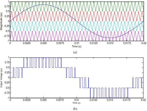
Figure8 PD-PWMtechnique:a)Referenceandcarriersignals, b)Outputphasevoltagewaveform
4.1 ANALYSIS AND DESIGN
Multilevel inverters (MLI) are being considered as the most popular method to synthesize almost sinusoidal waveforms using multi steps. Out of three conventional topologies cascaded H- bridge type of MLIs with different dc sourcesareproventobemorereliableingeneratinghighervoltagewithcomparativelylessharmonicsduetoitsmodular nature.ThesetypesofMLIsarealsoverysuitableforsolarapplicationsastheseparatedcsourcesrequirementisnaturally available.However,therearecertaindrawbacksoftheseMLIssuchastheuseoflargenumberofswitchesandtherelated gate drive circuit design as required by the corresponding semiconductor switches which create more complexity in electricalandmechanicaldesignoftheinverters.
The design of cascaded MLIs can be made simple by designing a simple gate pulse generation scheme. The cascadedMLIs usebridgescascadedwitheachother. Fora fivelevel inverter,twobridgesarerequired,fora sevenlevel inverterthreebridgesarerequiredandforaninelevelinverterfourbridgesarerequiredandsoon.Onebridgeconsistsof four semiconductor switches, so the number of switches increase with the level and voltage steps. Hence the switching losses and the cost of the MLIs also increase accordingly. Therefore, an initiative is taken to reduce the number of semiconductorswitchesandhencethecostofMLIandasimplerswitchingtechniqueisdevelopedtocontroltheMLIs.In thissection,amethodisdevelopedtoreducetheswitchesforasevenlevelinverterbyusing6switches.
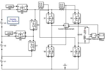
In this topology six MOSFETS are used. Four MOSFETS are used in H-bridge for changing the polarity and two MOSFETS are used for level generation. Two diodes are used to generate voltage ±V. The switching scheme is given in Table-1. It has 7 output voltage levels that is 3V, 2V, V, 0, -V,-2V, -3V. For 3V output voltage, MOSFETS S1, S4 & S7 are switched on and others are switched off. For 2V output voltage, MOSFETS S1, S4 & S6 are switched on and others are switchedoff.ForVoutputvoltage,twoMOSFETSS1andS4areonlyswitchedonandothersareswitchedoff. For0output voltagealltheMOSFETSareswitchedoff.For-Voutputvoltage,twoMOSFETSS2,S3areonlyswitchedonandothersare switched off. For -2V output voltage, MOSFETS S2, S3 & S6 are switched on and others are switched off. For -3V output voltage,MOSFETSS2,S3& S7areswitchedonandothersareswitchedoff.Itcan beobservedthattheswitchingdevices for the proposed seven level seven switch inverter at the time of conduction are three and for seven level six switch inverteris2or3.Soswitchinglossisgreatlyreduced.Table4.1representstheswitchingschemeoftheproposedtopology
Table 1 Switching scheme for 7-level 6-switch topology
1 OFF OFF ON OFF ON OFF +Vdc
2 OFF ON OFF OFF ON OFF +2Vdc
3 ON OFF OFF OFF ON OFF +3Vdc
4 OFF OFF OFF OFF OFF ON 0
5 ON OFF OFF ON OFF OFF Vdc
6 OFF ON OFF ON OFF OFF 2Vdc
7 OFF OFF ON ON OFF OFF 3Vdc
The pulse generation is essential in order to trigger the switches with appropriate pulse pattern to produce the desired7-level output.Itisinevitabletoanalysewhich PWMsuitsthe newtopology.Thesimplest PWMtechniqueisthe carrier-basedPWM(CBPWM)technique.ItcanbefurthercategorizedintolevelandphaseshiftingCBPWMs,respectively. SincethephaseshiftingCBPWMyieldsmoreharmonicscomparatively,thelevelshiftingCBPWMispreferredoverit.
The reference signal comparing with carrier generating pulse which is then modified feeding to logic gates in ordertogettherequiredpatterntotrigger theswitches attheproperinstant.For examplesswitchesS1needstohavea pulse so as to obtain +Vdc and −3Vdc and S2 requires +2Vdc and −2Vdc. S3 conducts +3Vdc and −Vdc. Also, switches S5 and S4 conduct positive and negative half cycles, respectively. Figure 4.2 represents the CBPWM technique proposed in thiswork.
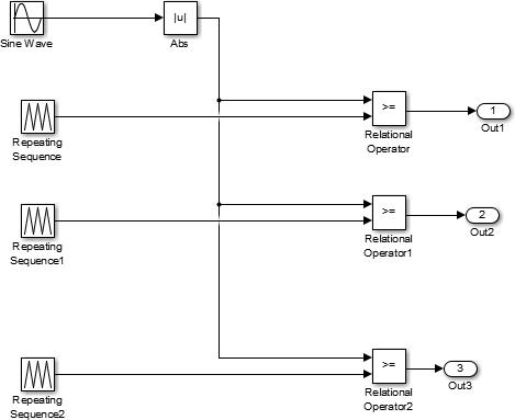
Figure11PWMgenerationscheme
5.1 EXPERIMENTAL
The simulation result and THD of the proposed topology is shown below. Here the input voltage is about 77V and the resistive load is taken. Figure 4.3 shows the output voltage waveform of the 7 level symmetrical CHB configuration. The magnitude of the voltage is is about 230 volts. The total harmonic distortion (THD) for the output voltage wave form is measured17.98%andisshowninfigure4.4.
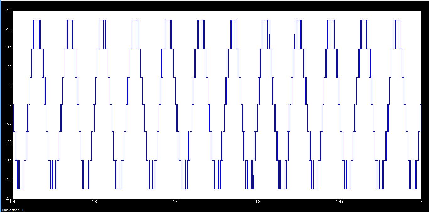
Table 2 : THD results obtained for conventional & modified 7 level inverter configurations
Symmetric conventional cascaded 7-level MLI
(7-level, 6 switches)
Simulationresultspresentedintable2(revealsthatthetotalharmonicdistortionisreducedto17.98%)
Table 3 Voltage stress in proposed topology across switches
Parameter
Table 4 Comparison of proposed 7-level with other topology
International Research Journal of Engineering and Technology (IRJET) e-ISSN:2395-0056
Volume: 11 Issue: 04 | Apr 2024 www.irjet.net p-ISSN:2395-0072
Inthischapter,theoverallconclusionalongwiththesuggestionsforfutureworkispresented.Inrecentdays MLI has drawn large interest in high power industry. They present a latest set of aspects to facilitate and utilized in reactive powercompensation.Theuniquearrangementofmultilevelvoltagesourceinvertersallowthemtoachievehighvoltages withthelowharmonicsnotincludingtheutilizationoftransformersorseriesconnectedsynchronizedswitchingdevices.
The Diode clamped, Flying capacitor, Cascaded H-bridge inverter are the three main different multilevel inverter structures which are used in industrial applications with separate dc sources. In flying capacitor and diode-clamped inverter there is a problem of capacitor voltage balancing and this problem is overcame by cascaded H-bridge inverter. However, the main drawback in Conventional cascaded is that when levels are increasing it requires more number of semiconductor switches. As a result some alternations are to be made in order to reduce the size and switch of the inverter.
Asinglephase7levelreducedswitchMLItopologyisintroduced anditsvariousmodesofoperationarestudied.Anovel modulationapproachispresentedandutilizedintheproposedtopology.Fromtheresults,itisevidentthatthisproposed systemreducesswitchinglosseswithlessTHD.Thus,theoverallcostreductionandeffectivereductionoftotalharmonics distortionisachieved.
1. Adam,GP,Anaya-Lara,O,Burt,GM,Telford,D,Williams,BW&McDonald,JR2010,‘Modularmultilevelinverter:pulse widthmodulationandcapacitorbalancingtechnique’,IETPowerElectronics,vol.3,no.5,pp.702–715.
2. Ammar Masaoud, Hew Wooi Ping, Saad Mekhilef & Hamza Omar Belkamel 2014, ‘A New Five- level Single-phase Inverter Employing a Space Vector Current Control’, Electric Power Components and Systems, vol. 42, no. 11, pp. 1121-1130.
3. Anup Kumar Panda & Sushree Sangita Patnaik 2015, ‘Analysis of cascaded multilevel inverters for active harmonic filteringindistributionnetworks’,ElectricalPowerandEnergysystems,vol.66,pp.216-226.
4. AtaollahMokhberdoran&AliAjami2014,‘SymmetricandAsymmetricDesignandImplementation ofNewCascaded MultilevelInverterTopology’,IEEETransactionsonPowerElectronics,vol.29,no.2,pp.6712-6724.
5. Bakhshizadeh Dowlatabadi, M, Iman-Eini, H & Blaabjerg, F 2015, ‘Selective Harmonic Elimination in Asymmetric Cascaded Multilevel Inverters Using a New Low-frequency Strategy for Photovoltaic Applications’, Electric Power ComponentsandSystems,vol.43,no.8-10,pp.964-969.
6. Banerjee, P,Biswarup Das &Agarwal,P2010, ‘Distribution Grid VoltageControl UsingCascadedMulti-level Inverter basedStaticSynchronousCompensator’,ElectricPowerComponentsandSystems,vol.38,pp.1389-1405.
7. Basavaraja,DS,Kulkarni,AD&Anandhapadmanabha,T2015,‘AModularSingle-PhaseMultistringMultilevelInverter TopologyforDistributedEnergyResources’,ProcediaTechnology,vol.21,pp.569-574.
8. Calais,M,Borle,LJ&Agelidis,VG2001, ‘Analysisofmulticarrier PWM methodsfor single- phase five level inverter’, Proceedingsof32nd AnnualIEEEInternationalPowerElectronicsSpecialistsConference(PESC’2001),pp.1351-1356, Vancouver,BC.
9. CharlesIkechukwuOdeh2014,‘AcascadedMulti-levelinverterTopologywithImprovedModulationScheme’,Electric PowerComponentsandsystems,vol.42,no.7,pp.768-777
10. EbrahimBabaei,MohammadFarhadiKangarlu&MehranSabahi2014,‘DynamicvoltagerestorerbasedonMultilevel InverterwithadjustableDc-linkvoltage’,IETPowerElectronics,vol.7,no.3,pp.576-590.
11. Ebrahim Babaei,Sara Laali &Sepideh Bahravar2015, ‘Anew CascadedMulti –level Inverter Topology with Reduced Number of Components and Charge Balance Control Methods Capabilities’, Electric Power Components and systems, vol.43,no.19,pp.2116-2130.
12. EbrahimBabaei,SaraLaali&ZahraBayat2015,‘ASingle–PhaseCascadedMultilevelInverterBasedonaNewBasic Unit With Reduced Number of Power Switches’, IEEE Transactions on Industrial Electronics, vol. 62, no. 2, pp. 922929.
International Research Journal of Engineering and Technology (IRJET) e-ISSN:2395-0056
Volume: 11 Issue: 04 | Apr 2034 www.irjet.net p-ISSN:2395-0072
13. Fei Jiang, Chunming Tu, Zhikang Shuai, Miaomiao Cheng, Zheng Lan & Fan Xiao 2016, ‘Multilevel Cascaded -Type DynamicVoltageRestorerWithFaultCurrent-LimitingFunction’,IEEETransactiononPowerDelivery,vol.31,no.3, pp.1261-1269.
14. Fernao Pires, V, Joao Fialho & Fernando Silva, J 2015, ‘HVDC transmission system using multilevel power converters basedondualthree-phasetwo-levelinverters’,ElectricalPowerandEnergysystems,vol.65,pp.191-200.
15. Gayathri Devi, KS, Arun, S & Sreeja, C 2014, ‘Comparative Study on different five level inverter topologies’, Electrical PowerandEnergySystems,vol.63,pp.362-372.
16. Govindaraju,G &Baskaran,K2011, ‘Sequential SwitchingHybrid Single- Carrier Sinusoidal Modulation forCascaded Multi-levelInverter’,ElectricPowerComponentsandsystems,vol.39,no.4,pp.303-316.
17. Gowande,SP&Ramteke,MR2014,‘Three-levelNPCinverterbasednewDSTATCOMtopologiesandtheirperformance evaluationforloadcompensation’,ElectricalPowerandEnergysystems,vol.61,pp.576-584.
18. Gupta, KK & Jain, S 2012, ‘Topology for multilevel inverters to attain maximum number of levels from given DC sources’,IETPowerElectronics,vol.5,no.4,pp.435-446.
19. HosseiniAghdam,MG,Fathi,SH&Gharehpetian,GB2008,‘ANovelSwitchingAlgorithmtoBalanceConductionLosses in Power Semiconductor Devices of Multi-level Cascade Inverters’, Electric Power Components and Systems, vol. 36, no.12,pp.1253-1281.
20. JunfengLiu,Cheng,KWE&YuanmaoYe2014,‘ACascadedMultilevelInverterBasedonSwitched-CapacitorforHighFrequencyACPowerDistributionSystem’,IEEETransactionsonPowerElectronics,vol.29,no.8,pp.4219-4230.
21. Khounjahan,H,Banaei,MR&AmirFarakhor2015,‘Anewlowcostcascadedtransformermultilevelinvertertopology using minimum number of components with modified selective harmonic elimination modulation’, Ain Shams EngineeringJournal,vol.6,pp.67-73
22. Krishna Kumar Gupta, Alekh Ranjan, Pallavee Bhatnagar, Lalit Kumar Sahu, & Shallendra Jain 2016, ‘Multilevel InverterTopologiesWithReducedDeviceCount:AReview’,IEEETransactionsonPowerElectronics,vol.31,no.1,pp. 135-151.
23. Krismadinata,NasrudinAbdRahim,HewWooiPing&JeyarajSelvaraj2013,‘Eliminationofharmonicsinphotovoltaic seven-levelinverterwithNewton-Raphsonoptimization’,ProcediaEnvironmentalSciences,vol.17,pp.519-528.
24. Kumar, GKN & Pal, Y 2014, ‘A modified switching scheme for a new multi level inverter topology for fuel-cell microgrid’,ProceedingsofIEEE6th IndiaInternationalConferenceonPowerElectronics(IICPE),Kurukshetra,pp.1-6.
25. Law Kah Haw, Mohammad SA Dahidah & Haider AF Almurib 2014, ‘SHE-PWM Cascaded Multilevel Inverter with AdjustableDCVoltageLevelsControlforSTATCOMApplications’,IEEETransactionsonPowerElectronics,vol.29,no. 12,pp.6433-6444.
26. Mahalakshmi, R & Sindhu Thampatty, KC 2015, ‘Grid Connected Multilevel Inverter for Renewable Energy Applications’,ProcediaTechnology,vol.21,pp.636-642.
27. Mahmoud El-Bakry 2014, ‘A 43 –Level filterless CMLI with very low harmonics values’, Journal of Electrical systems andInformationTechnology,vol.1,pp.175-186.
28. McGrath BP & Holmes DG 2000, ‘A comparison of multi carrier PWM strategies for cascaded and neutral point clamped multilevel inverters’, Proceedings of 31st IEEE International Power Electronics Specialists Conference (PESC’2000),pp.674-679,Galway.