Enhancing Full Adder Efficiency for Low-Power Applications in 32nm CMOS Technology
Shilpa More1, Gagandeep S. Dhir2, Ramandeep S. Dhir3
1 ,2
Research Scholar, 3Ass.Prof Department of EEE Savitribai Phule Pune University, Pimpri.
Abstract:
The partial drive designed for improved speed and compactness of CMOS technology wants the uninterrupted innovation of progressive features and procedures. However, there are no encouraging applicants who can exchange CMOS with improved performance and high-density addition for the moment. CMOS skills for lofty presentation analogue application in conditions of speed-to-power indulgence, tool competence with warm electron inject entry present plan parameter. With the development of new materials also come new manufacturing challenges. We will also discuss the standing of relationship in the CMOS commercial model. The effort, hence, prove the efficiency of GEWE-RC forRFICs bysuperiorcompetence, enhanced speedpower dissipationperformance; andthus, inthedesign and modelling of power amplifiers. This performance valuation is supported out spending ATLAS device simulator.
Keywords—CMOS technology, Mathematical model, characterization vehicles, deep sub micrometer processes
1. INTRODUCTION
A widely adopted and highly regarded MOSFET technology in usetoday isthecomplementary metaloxide-semiconductor (CMOS) technology. CMOS has become the cornerstone of modern semiconductor design, powering a vast array of devices, including microprocessors, memory units, and application-specific integrated circuits (ASICs). Its versatility and energy efficiency have made it the preferred choiceforcreatinghigh-performance,lowpower electronic systems across industries. Grading of MOS transistor scopes is a key feature in the upgrading of performance of CMOS technologies. Thispowerefficiencycanbeattributedtoaquadratic reduction of switching charge, linear increase in
speed, and linear decrease in supply voltage. At the similar time, transistor region decrease quadraticaly. The tendency show a deliberate enhance in expire region which means that the numeral of transistors increase at least quadraticaly.
CMOS delivers the essential individualities required for high-density reason plans. Moreover, with recent advances in the field of Bi CMOS, it is projected that we have a tools which will afford a conversion to the next period
2. PROPOSED DESIGN
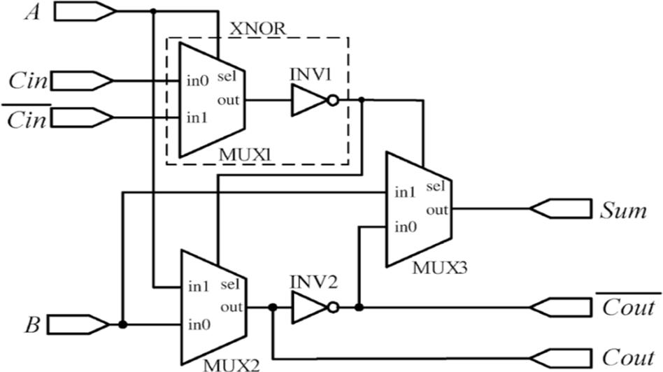
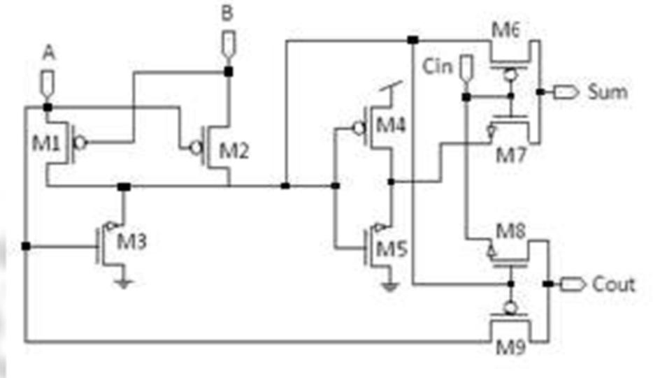
Thedesign isbasically divided into threebuilding blocks. In this design one XNOR gate, two multiplexer circuits and oneinverter has present and
these entire combined make a full adder circuit and perform operations of binary addition.
The significance of short-circuit control indulgence in CMOS buffer, come from the information that a huge part of the power dissolute in VLSI circuit is due to on-chip with off-chip indication driver trails, which are based on inverting buffers. Another projected plan, filled adder circuit is realize through by component 1 & component 2as 2 XNOR gate with component 3 as 2:1 MUX. The planned XNOR unit is intended by inverter plus one NMOStransistorareusedtoobtaintheamountwhile production of this unit is once more process by an extra comparable component and MUX is used to obtain carry


XNOR WORKING
In this plan method filled adder formation is intended via contravention the filled adder into three modules. Module 1 is an XOR-XNOR circuit which drive the extra module; therefore it should contain superior dynamic ability plus provide occupied swing output concurrently.
For A=1 & B=1, P1 & N2 will beoff & N1 will be on, duetowhichtheoutputnodewillbehighasthere is no conducting path from output node to ground. There will be a threshold drop in the N1 and to maintain the high output swing and reduce the threshold voltage drop and to reduce time delay, channel width of N1 can be increased. There aretwo XNOR gates which are cascade toward create the SUM.
MUX WORKING
A multiplexer (MUX) is a device that selectively routes one of many input signals to a single output based on a control line. It functions as an electronic switch, enabling high-speed data transmission by choosing the appropriate signal path. A basic, nonelectronic representation of a multiplexer can be found in a single-pole, multi-position switch, which manually directs a single input to one of several output positions. In the realm of digital electronics, multiplexers play a vital role in enabling high-speed switching, allowing multiple data sources to be efficiently routed to a single output.
In the context of MOS technology, there are two primary types of MOS transistors: NMOS and
PMOS. An NMOS transistor efficiently pulls the output to a "LOW" state but struggles with performance when transitioning to a "HIGH" state. Similarly, a PMOS transistor excels in pulling the output to "LOW," but its performance diminishes when it needs to drive a "HIGH" signal. These characteristics influence the design and efficiencyof circuitsutilizing both typesof transistors. MUX isas exposed into this circuit is planned with the assist of general NAND gates where 7 PMOS and 7 NMOS are used. The whole numbers of 14 transistors are used in the CMOS plan P button islinked toward the Vdd to the output as well as N button is linked toward the output to Vss. In this CMOS design NMOS works as pull down network and PMOS works as pull up network.
SIMULATION

COMPARATIVE ANALYSIS
In this article control plus region expenditure for the auto generate design, half tradition intended plan with completely convention planned outline of XOR withXNORbasedfullsubtracterhasbeencompared.
The XOR along with XNOR circuit can be implemented within dissimilar architectures through by dissimilar circuit designs. These articles evaluate as well as contrast the presentation of a variety of drawing technique of XOR-XNOR circuits. In today's electronic industry, one of the most critical parameters is low power consumption. To develop devices that are more reliable and efficient, it is essential to minimize power usage. As the demand forportableconsumerelectronicsrisesandchipsizes continue to shrink, managing power dissipation becomes increasingly challenging.
For CMOS circuits, power consumption must be minimized for two primary reasons:
Thermal management: The primary goal is to reduce heat generation, allowing a higher density of functions to be integrated onto a single IC chip without compromising performance or stability.
Energy efficiency: With smaller and more complex devices, lowering power consumption ensures longer battery life and reduced energy demands, key factorsforthenextgenerationofportableelectronics.
Any quantity of control utilization is productive as lengthy as it doesn’t disgrace generally circuit presentation.
The second key factor in minimizing power consumption is ensuring optimal performance in battery-operated devices. By selecting the right design approach, thepower efficiency of circuitscan be significantly enhanced at the design stage. Without implementing low-power design strategies,
devicesoftenfacetheissueofrapidbatterydepletion. Furthermore, packaging and cooling solutions become more complex and costly, creating significant challenges in maintaining performance. This, in turn, leads to an unavoidable rise in the overall cost of the device, making power management a crucial consideration in modern electronics development.
CONCLUSION
The continuous miniaturization of the CMOS technology resulted in ultra fast processors and will also degrade the device performance due to Short Channel Effects (SCEs). In order to overcome these problems, various device engineering techniques were proposed like source drain engineering (LDD MOSFET) lateral channel engineering (i.e. graded guide MOSFET, corona and Dielectric pouch MOSFET), entry dielectric manufacturing (i.e. gateway pile MOSFET), substrate manufacturing (i.e. Silicon On Insulator with Silicon On not anything MOSFET) plus gateway electrode manufacturing (i.e. twice gateway MOSFET). The effort obtainable in this exposition was mostly focused on Dielectric pouch MOSFET from side guide manufacturing, Silicon On not anything MOSFET from substrate manufacturing as well as twice gateway MOSFET from gateway electrode manufacturing technique that can beat the demerits linked by size MOSFET along with too offer get better machine presentation. Conservative CMOS manufacture process have supported numerous
generation of diminution, through each new manufacture bring predictable compensation into conditions of price, velocity as well as power utilization. There will probably exist variation resting on CMOS circuit, except rejection essential move into circuit kind seem towards on the outlook.
REFERENCE
1. B. Dilli kumar, K. Charan kumar , M. Bharathi, “Low power multiplexer based full adder using pass transistor logic”, International Journal of Advanced Research in Computer Engineering & Technology Volume 1, Issue 5, July 2012, pp. 291-296.
2. Hanho Lee and Gerald Soblman, “A new low_voltage full adder circuit”, IEEE International Symposium on Circuits and Systems, 1997, pp. 88-92.
3. Pranshu Sharma, Anjali Sharma, Richa Singh, “ Design and Analysis of Area and Power Efficient 1-Bit Full Subtractor using 120nm Technology”, International Journal of Computer Applications Vol.88, No.12, February 2014, pp. 36-42.
4. E. Grossar, M. Stucchi, K. Maex, W. Dehaene, “Read stability and write-ability analysis of SRAM cells for nanometer technologies.” IEEE Journal of Solid-StateCircuits, vol. 41, no. 11, pp. 2577-2588, 2006.
5. M.Khare et al., "A high performance 90nm SOI technology with 0.992 mm2 6T-SRAM cell", Proc. Intl. Electron Devices Meeting, pp. 407–410, 2002.
6. Neil H. E. Weste, David Money Harris, "CMOS VLSIDesignACircuits andSystemsPerspective - 4th Edition", Pearson Education, 2011.
7. 1. S.-M. Kang and Y. Leblebici, “CMOS Digital Integrated Circuits: Analysis and Design”, McGraw Hill, 2002.
8. Suman Nehra and P. K. Ghosh, “Design of a Low Power XNOR gate Using MTCMOS Technique”, Advance in Electronic and Electric Engineering. ISSN 2231-1297, Vol. 3, Number 6 (2013), pp. 701-710.
9. Narendra, S.G. Challenges, Design Choices in nanoscale CMOS. ACM J. Emerg. Technol. Comput. Syst. 2005, 1, 7–49.
10. Sill, F.; You, J.; Timmermann, D. Design of Mixed Gates for Leakage Reduction. In Proceedings of the 17th ACM Great Lakes Symposium on VLSI, New York, NY, USA, 11–13 March 2007.
11. Smayling, M.; Axelrad, V. Simulation-Based Lithography Optimization for Logic Circuits at 22 nm and Below. In Proceedings of the International Conference on Simulation of Semiconductor Processes and Devices, SISPAD ’09, San Diego, CA, USA, 9–11 September 2009; pp. 1–4.
13. Shauly, E.; Parag, A.; Khmaisy, H.; Krispil, U.; Adan, O.; Levi, S.; Latinski, S.; Schwarzband, I.; Rotstein, I. Standard cell electrical and physical variability analysis based on automatic physical measurement for design-for-manufacturing purposes. Proc. SPIE 2011, doi:10.1117/12.881841.
14. Shahidi, G.G. Design-Technology Interaction for Post-32 nm Node CMOS Technology. In Proceedings of the 2010 Symposium on VLSI Technology (VLSIT), Honolulu, HI, USA, 15–17 June 2010; pp. 143–144.
12. Arnaud, F.; Boeuf, F.; Salvetti, F.; Lenoble, D.; Wacquant, F.; Regnier, C.; Morin, P.; Emonet, N.; Denis, E.; Oberlin, J.C.; et al. A Functional 0.69 μm2 Embedded 6T-SRAM bit cell for 65 nm CMOS platform. In Proceedings of the 2003 Symposium on VLSI Technology, Kyoto, Japan, 10–12 June 2003; pp. 65–66.
