
7 minute read
Semiconductors


vehicles. Atechnician must have a thorough grasp of the basis of electronics, it has become the single most important subject area, and the days when technicians could avoid working on an electronic circuit throughout an entire career are long past. This course of study will begin with semiconductor components.
Chapter 3examined the atom’s valence ring, the outermost electron shell. We learned that elements whose atoms have three or fewer electrons in their valence rings are good conductors because the free electrons in the valence ring readily join with the valence electrons of other, similar atoms. We also learned that elements whose atoms have five or more electrons in their valence rings are good insulators (poor conductors) because the valence electrons do not readily join with those of other atoms.
Elements whose atoms have four electrons in their valence rings are neither good insulators nor good conductors. Their four valence electrons cause special electrical properties, which give them the name semiconductors. Germanium and silicon are two widely used semiconductor elements. Semiconductors are materials with exactly four electrons in their outer shell, so they cannot be classified as insulators or conductors. If an element falls into this group but can be changed into a useful conductor, it is a semiconductor.
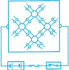
When semiconductor elements are in the form of a crystal, they bond together so that each atom has eight electrons in its valence ring: It has its own four electrons and shares four with surrounding atoms (Figure 10-1). In this form it is an excellent insulator, because there are no free electrons to carry current flow. Selenium, copper oxide, andgallium arsenide are all semiconductors, but silicon and germanium are the most commonly used. Pure semiconductors have tight electron bonding; there’s no place for electrons to move. In this natural state, the elements aren’t useful for conducting electricity.
Other elements can be added to silicon and germanium to change this crystalline structure. This is called doping the semiconductor. The ratio of doping elements to silicon or germanium is about 1 to 10,000,000. The doping elements are often called impurities because their addition to the silicon or germanium makes the semiconductor materials impure.
Figure 10-1. Crystalline silicon is an excellent insulator.
(Delphi Automotive Systems)
Semiconductor Doping
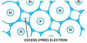
Pure silicon has four electrons in the outer orbit, which makes it a semiconductor. However, the silicon must be very pure without any impurities that can affect its electrical properties. Pure silicon is a crystal that can be created by heating silicon in an electric oven called silicon crystal growers. See Figure 10-2.To make this pure silicon useful for electronic devices, a controlled amount of impurities are added to the pure silicon during the growing process. The amount of the impurities is extremely small. The process of adding impurities to pure silicon is called doping. If an element that has only three electrons in the outer orbit, such as boron, is combined with the silicon, the result is a molecule that has an opening, called a hole. While the resulting semiconductor is still electrically neutral, this vacant area is a place where an electron could fill. This type of material is called P-type material. If the pure silicon is doped using an element with five electrons in its outer orbit, such as phosphorus, the resulting semiconductor material is called N-type
material.
HISTORICAL NOTE:While the properties of semiconductors have been known since the late 1800s,it was not until the 1930s that silicon and germanium could be produced pure enough to allow accurate control of the doping process.An electric oven is used because it does not use any fuel,and there are no impurities from the heating fuel that could affect the process.
P- and N-Type Material
If there is an excess of free electrons, the semiconductor is N-type material, where N stands for negative. If there is a shortage of free electrons, the semiconductor is P-type material, where P stands for positive. Figure 10-3shows P- and N-type materials together. In a conductor, we describe current flow as the movement of electrons, in a semiconductor, something else is going on. Just as in a conductor, there is a movement of free electrons, but at the same time, there is a movement of “holes.”
Besides silicon, another semiconductor material, germanium, can be used and doped the same way as silicon.
If silicon or germanium is doped with an element such as phosphorus, arsenic, or antimony, each of which has five electrons in its valence ring, there will not be enough space for the ninth electron in any of the shared valence rings. This extra electron is free (Figure 10-4). This type of doped material is called negative or N-type material because it already has excess electrons and will repel additional negative charges.
Doping of a semiconductor material, using an element with three electrons in its outer shell called trivalent, results in P-type material. Using an element with five electrons in its outer orbit, called pentavalent, results in N-type material.
If silicon or germanium is doped with an element such as boron or indium, each of which has only three electrons in its outer shell, some of the atoms will have only seven electrons in their valence rings. There will be a hole in these valence rings (Figure 10-5). This type of doped material is called positive or P-type material, because it will attract a negative charge (an electron). In different ways, P-type and N-type silicon crystals may permit an electrical current flow: In the P-type semiconductor, current flow
Si Si
Si SHARED ELECTRONS
Si
Figure 10-2. Germanium atom in a crystallized cluster with shared electrons.
P-TYPE N-TYPE
Material excess holes (+) Material excess electrons (-)

Figure 10-3. P- and N-type material. Figure 10-4. N-type material has an extra, or free,
electron. (Delphi Automotive Systems)
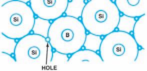
Figure 10-5. P-type material has a “hole” in some of
its valence rings. (Delphi Automotive Systems)
is occasioned by a deficit of electrons, while in the N-type semiconductor, current flow is occasioned by an excess of electrons.
PN-Junction
When the two semiconductor materials are brought together, as shown in Figure 10-6, something happens at the area where the two touch. This area is called the PN junction. You chemically join P- and N-type materials either by growing them together or fusing them with some type of heat process. Either way they join together as a single crystal structure. The excess electrons in the N-type material are attracted to the holes in the P-type material. Some electrons drift across the junction to combine with holes. As an electron combines with a hole, both effectively disappear. Whenever a voltage is applied to a semiconductor, electrons will flow towards the positive terminal and the holes will move towards the negative terminal. The electron is nolonger free and the hole no longer exists. Because of the cancellation of charges, the material at the junction assumes a positive charge in the N-type material and a negative charge in the P-type material; PN-junctions become diodes.
As long as no external voltage is applied to the semiconductors, there is a limit to how many electrons will cross the PN junction. Each electron that crosses the junction leaves behind an atom that is missing a negative charge. Such an atom is called a positive ion. In the same way, each hole that crosses the junction leaves behind a negative ion. As positive ions accumulate in the N-type material, they exert a force (a potential) that prevents any more electrons from leaving. As negative ions accumulate in the P-type material, they exert a potential that keeps any more holes from leaving.
Eventually, this results in a stable condition that leaves a deficiency of both holes and electrons at the PN junction. This zone is called the depletion region. The potentials exerted by the negative and positive ions on opposite sides of the depletion region are two unlike charges. Combining unlike charges creates voltage potential. The voltage potential across the PN junction is called the barrier voltage. Doped germanium has a barrier voltage of about 0.3 volt. Doped silicon has a barrier voltage of about 0.7 volt.
Free Electrons and Movement of Holes
In P-type semiconductor material, there is a predominance of acceptor atoms and holes. In N-type material, there is a predominance of donor atoms and free electrons. When the two semiconductors are kept separate, holes and electrons are distributed randomly throughout the respective materials. Ahole is a location where an electron normally resides but is currently absent. Ahole is not a particle, but it behaves like one (Figure 10-7).
Because a hole is the absence of an electron, it represents a missing negative charge. As a result, a hole acts like a positively charged particle. Electrons and holes occur in both types of semi-
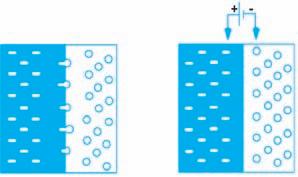
Figure 10-6. PN junction.
Movement of Marbles / Electrons
Movement of Holes
Figure 10-7. Movement of holes. (GM Service and
Parts Operations)


