7 minute read
Novel monolithic Si NEMS

The bigger picture of miniaturisation
©ESA
Microelectromechanical systems (MEMS) are an important part of many technologies, now researchers are looking towards the development of even smaller systems, nanoelectromechanical systems (NEMS). Silicon nanowires are an important component of such NEMS, and a deeper understanding of their crystalline structure is crucial to further developments, as Professor Antonia Neels explains.
The ongoing miniaturisation of microelectromechanical systems (MEMS) in the digital age has opened up new commercial possibilities, and MEMS today are applied in a wide range of devices, including sensors and actuators with both electrical and mechanical functions and characteristics. The structure of the materials used in these systems helps to define their overall properties, and a deeper understanding could point the way towards the development of even smaller nanoelectromechanical systems (NEMS) in future, a topic at the heart of Professor Antonia Neels’ research. “Silicon may behave very differently in nano-structures than in micro-systems, because a lot of physical properties change when you go to the nanolevel,” she outlines. Based at Switzerland’s Federal Laboratories (Empa), Professor Neels is the Principal Investigator of a research project seeking to link the structure and physical properties of silicon NEMS.
Silicon nanowires
A major priority in the project is the characterisation of silicon nanowires, a relatively new type of 1-dimensional nanostructure which can act as a core component of NEMS. Researchers in the project are looking at nanowires which are about 80 nanometres wide and a few microns long. “They are small and difficult to handle, and their structural and physical behaviour is very different compared to micrometer-sized device parts,” says Professor Neels. Two of the most notable characteristics of silicon nanowires are their strength and flexibility, which makes them well-suited for use in NEMS.
A significant degree of progress has been made over the last decade in combining silicon nanowires in devices, yet challenges still remain in terms of their application in novel monolithic NEMS. The architecture of these systems is often extremely complex and crystalline defects enter into nanowires and alter their properties, so sophisticated techniques are required to characterise them. “New technologies need new analytical tools,” says Professor Neels. Researchers in the project are using high-resolution X-ray diffraction (HRXRD) and other techniques to gain deeper insights into the structure of silicon nanowires. “HRXRD is dedicated to the analysis of semi-conductor materials, high-purity crystals, like single crystal silicon,” explains Professor Neels. The primary aim here is to relate the structure of a material to its performance and physical properties. Professor Neels and her colleagues develop X-ray based analytical methods suitable for the new materials structures that are emerging. During the fabrication of NEMS / MEMS, and also later on during their operation, strain, deformation and additional defects are introduced into the silicon crystal which may influence physical properties such as electrical or mechanical functioning. Some of these effects may be desirable, for example because they improve the electromechanical properties of the nanowire system, while others may be undesirable; Professor Neels aims to help build a deeper understanding in this respect.
This research involves investigating defects and the defect mobility, from which more can be learned about the expected lifetime of such
devices. An important part of the project’s research centres therefore around monitoring any changes in the structure over time, a topic Professor Neels plans to address in the second half of the project’s funding term. “We plan to monitor the effects of electrical actuation of the nanowire structure, and investigate any structural changes,” she says. This will also have an impact on the durability and reliability of nanowires, both of which are important considerations in terms of the possible applications of these systems. “Reliability is very important in any application but especially in biomedicine and space,” stresses Professor Neels. “We can address accelerated aging processes, and see how things like
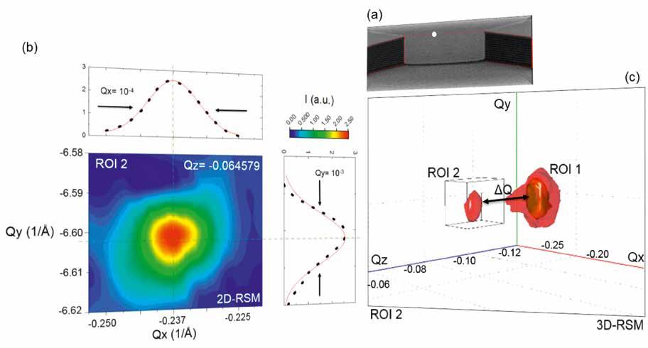
HRXRD on the Si nanowire system (a): determination of silicon strain gradients and lattice tilts trough Reciprocal Space
Mapping (RSM) relative to the scan point on the Si nanowire (a) (white point). RSMs in one, two (b) and three (c) dimensions. temperature changes will affect the structure, and consequently its physical properties.”
Applications
MEMS currently available on the market are pretty stable in terms of performance, and are applied in a wide variety of sectors. However, researchers are still working to further miniaturise these systems, which Professor Neels says will bring some important benefits. “The important thing is that we can monitor smaller effects, so we can be much more precise with these nano-systems than we can with micro-systems,” she explains. The nanosystems could be used to improve performance in established applications, while their heightened sensitivity could also open up new possibilities. “With NEMS, new applications become possible that can’t really be approached with microsystems, because we can sense really very small quantities, for example of radiation or molecules,” continues Professor Neels. “Important possible application domains of NEMS include space applications and biomedicine.”
At this stage however Professor Neels’ priority is more to investigate the structure of silicon nanowires, and look at how they are affected by the fabrication process. This includes not just analysing defects and strains introduced during the manufacturing process, but also defects related to the overall environmental conditions and operations. “There is a degradation over time, as defects will also be introduced into a system from the environment. We are working on defect analysis,” says Professor Neels. A deeper understanding of the fundamental structure of nanowires and the defects within them is essential to their wider application, which is an important motivation behind Professor Neels’ research.
The project’s research could hold important implications for the commercial sector, enabling the development of more effective, sensitive NEMS in future. Professor Neels’ group is very active in the biomedical domain in particular, while she says there are also many other possible application domains. “The space domain would be very interesting, while the domestic domain is also highly relevant, as silicon is very robust,” she says.
Single structure like-NEMS based Si NWs obtained from a silicon wafer. The NW has a width of 80 nm and a length of 12 μm, and 5.5 μm suspended from the beneath substrate.

Sketch of the experimental setup for a horizontal Bragg diffraction configuration. Scans were performed by moving the sample along the y and z-axis directions. Ki is the incident wave vector, Kt is the transmitted vector and Ks is the scattered vector. Qx, Qy and Qz are the coordinates in reciprocal space.
Array of suspended Silicon-nanowires. The total size of the microchip is 500 x 500 μm. It includes 450 Si-NWs of 160 nm width and 10 μm long, and 10 μm suspended from the beneath substrate.


Novel monolithic Si NEMS Novel monolithic Si NEMS: Study and correlation of structural and physical behaviour Project Objectives
This study brings forward the understanding of the Si-nanowires structures in the field of nano and microelectromechanical systems (NEMS & MEMS) for potential sensing application in space, biomedical, earth and environmental sectors. This will enable us to understand the relationship between the physical properties and the silicon crystal lattice, and do correlations with the fabrication process and mechanical behavior of silicon nanowires under service condition.
Project Funding
The project is granted by the Swiss National Science Foundation, Grant No. 169257, and includes the funding of the doctoral thesis of Simone Dolabella who contributes with a great success to this topic. https://doi.org/10.1107/S1600576719015504
Project Partners
We collaborate with scientists from the beamline ID01 at the ESRF in Grenoble, France and the Koc University in Istanbul, Turkey.
Contact Details
Prof. Dr. Antonia Neels, Titular Professor Head Center for X-ray Analytics Empa - Swiss Federal Laboratories for Materials Science and Technology Überlandstrasse 129, 8600 Dübendorf, Switzerland T: +41 58 765 45 07 E: antonia.neels@empa.ch W: http://www.empa.ch/x-ray W: https://www.empa.ch/ documents/56073/9770737/Simone_ Poster+website_final.pdf/ de895c94-a51f-4dbb-bdb8- 8d9d533a2f94 W: www.empa.ch
Professor Antonia Neels
Professor Antonia Neels obtained her PhD in Science from the University of Neuchâtel (CH), has been leading the XRD laboratory at CSEM (CH) and received an Executive MBA in Management of Technology (MoT) from the EPFL. Since 2014, she heads the Center for X-ray Analytics at Empa. Since 2018, Antonia Neels is appointed Titular Professor at the University of Fribourg. She is experienced in the development of X-ray based analytical methods.