
AM-Receiver Project
ByGabeEsquibelandDjangoDemetri [EE-334]
Abstract:
The project consists of designing anAM receiver via theoretical analyses, LTSpice, and breadboard prototyping Asecond order passive bandpass filter, a BS170 common source used as a buffer, a 2N3904 common emitter used as an amplifier, a single 1N4148 diode mixer, and a second order passive low pass filter were the chosen components The final circuit was able to correctly filter, amplify, and mixAM signals but not reliably
Introduction:
The project consists of designing anAM receiver via theoretical analyses, LTSpice, and breadboard prototyping.TheAM receiver consisted of a band pass and low pass filter, a low noise amplifier, and a mixer The components used were ceramic and electrolytic capacitors, molded inductors, a BS170, a 2N3904, a 1N4148, potentiometers, BS880 breadboards, dc power supply, and twoAgilent two channel oscilloscopes.

Figure 1: Ablock diagram showing all the components used for theAM receiver, including a band pass filter, low noise amplifier, mixer, and low pass filter
Band Pass Filter Values:
Table 1: Atable consisting of the simulated values for the corner and center frequencies as well as the voltage ratio, in kHz for the band pass filter.
First Corner Frequency (kHz) Second Corner Frequency (kHz)
Frequency (kHz)
Table 2: Atable consisting of the measured values for the corner and center frequencies as well as the voltage ratio, in kHz for the band pass filter
First Corner Frequency (kHz) Second Corner Frequency (kHz)
Buffer Values:
Table 3: Atable consisting of the simulated nodal voltages, biasing voltage, current, MOSFET transconductance parameter, output and input resistances, and gain for the buffer
Table 4: Atable consisting of the measured nodal voltages, biasing voltage, current, MOSFET transconductance parameter, output and input resistances, and gain for the buffer
Gain Cell Values:
Table 5: Atable consisting of the simulated nodal voltages, currents, beta, output and input resistances, and gain for the gain cell
Table 6: Atable consisting of the measured nodal voltages, currents, beta, output and input resistances, and gain for the gain cell
(V) Vb (V) Ve (V) Ic (mA)
Mixer Values:
(mA)
Table 7: Atable consisting of the four simulated resistor values and the biasing voltage for the mixer.
Table 8: Atable consisting of the four resistor values and the biasing voltage for the mixer.
Low Pass Filter Values:
Table 9: Atable consisting of the simulated values for the corner frequencies as well as the voltage ratio, in kHz for the low pass filter
Corner Frequency (kHz)
Table 10: Atable consisting of the measured values for the corner frequencies as well as the voltage ratio, in kHz for the low pass filter.
Corner Frequency (kHz)
Band Pass Filter:
Since radio stations broadcast multiple channels the first component needs to receive a single channel This selective behavior can be achieved by a bandpass filter
TheoreticalAnalysis:

Figure 2: Atheoretical analysis for a second order passive band pass filter Q, R, C and the transfer function are found and are used to design a filter for the project.Amore elaborate explanation is provided below
First, the circuit variables are converted from the time domain to the frequency domain, in terms of s The inductor and capacitor are combined in parallel to create Z2 Using the voltage division equation and solving for Vo(s)/Vi(s), the transfer function is found Since the receiver will operate in theAM range, the channel bandwidth is 8kHz. But in practice the standard is a bandwidth of 20 4kHz The expected frequency is 450kHz and is noted as the center frequency. Consequently, the first corner frequency is 439.8kHz and the second corner frequency is 460.2kHz. Since an inductor of 100µH is the only inductor available, Equation 2, (derived from Equation 1), is used to find the capacitance With these values the quality factor can be found using Equation 4, derived from the definition of second order filters’transfer function Finally, using Equation 3 the required resistance can be found, also derived from second order filters’transfer function
Equation 4 also implies the gain-bandwidth product, stating that the gain and bandwidth have an inverse relationship
Table11:Atableconsistingofthecalculatedvalues ofQ,R,andCfromthetheoreticalanalysis inFigure.
Simulation:

Figure3:LTspicesimulationofthedesignedpassiveband-passfilterwithcomponentsR1,C1, andL1.Thecircuitisfedwitha30mVpeak-to-peakacsignal.

Figure4:LTspiceac-analysisplottingthefrequencyresponseofthebandpassfilter.Center frequencyappearsat449.kHz.

Figure5:Zoomedinandmeasuredcenterfrequencyofthepassiveband-passfilter.Center Frequencyis449.8kHz


Figure6:Measuredcornerfrequenciesofbandpassfilterwithbandwidthhighlightedinblueon theright.
Table 12:Atable consisting of the simulated values for the capacitance, resistance, and inductance Inductor ( H)µ
The first decision was between an active or passive filter.The passive filter seemed like the obvious choice since it requires less components, less design, and less power The only concern was the gain loss that would occur through the filter The 3dB loss at the cutoff frequency equivalates to a 1.41V/V loss which seems pale in comparison with the benefits. For higher accuracy a second order filter was chosen Some experimentation led to the values found inTable 2
Table 13: Atable consisting of the simulated values for the corner and center frequencies as well as the voltage ratio, in kHz.
First Corner Frequency (kHz) Second Corner Frequency (kHz)
Design/Measurements:

Figure 7: The realized circuit of the passive band-pass filter using a series resistance for R1, band-pass output is Vo (bandpass) and input is V1.
Table 14: Atable consisting of the measured values of the inductor, capacitors, and resistor used in the breadboard circuit.
Table 15: Atable consisting of the measured values for the corner and center frequencies as well as the voltage ratio, in kHz
First Corner Frequency Second Corner
Assembly of the filter was straightforward with the exception of the capacitors First, there were no 1.25nF capacitors in our supply so at first a 15nF and 68nF were placed in series to obtain a value closer After some more thought simply using a 1 5nF capacitor with a high tolerance was simpler. Second, the center frequency is extremely sensitive to changes in the capacitance, a pattern realized while experimenting in LTSpice The closest value we could obtain was 1 23nF which is far from what is optimal for this circuit
Unsatisfied with the bandwidth, different resistances were tried in an attempt to modify the selectivity We determined the gain and bandwidth have an inverse relationship, confirming the gain-bandwidth product Since the starting signal is 30mV the loss of output voltage was a major concern and the group decided to sacrifice some precision to maintain as much gain as possible The original configuration was the best of both worlds The alternate values can be found inTable 6
Table 16: Alternate resistance values for the low pass filter and their resulting bandwidths and gains, in kΩ, kHz, and dB

Figure 8: Afrequency response plot with gain in dB on the y-axis and frequency plotted logarithmically on the x-axis, in kHz The first and second cut off frequencies are 431 0kHz and 464kHz respectively

Figure 9: Waveform of the passive bandpass filter’s input and output at 450kHz with a 1 05Vpp signal

Figure 10: Waveform of the passive bandpass filter’s input and output at 450kHz with theAM demo signal
Discussion:
Asmart first step would be to perform a sensitivity analysis for the filter in the theoretical analysis.After determining which, if any, components demand precision and how much then the purchasing of components could be implemented
Furthermore, the purchasing of a variable capacitor and inductor would not only allow us to better understand the sensitivity of the circuit but also obtain values closer to what needed. The final configuration gave a bandwidth of 33kHz and -3 774dB Although this was the best balance we could obtain for the filter we designed, these values could be improved greatly with a higher order filter, especially considering there is not a large gap in difficulty between second and fourth order passive filters
The center frequency is not correct but this is very likely due to the imprecise capacitors. Since the center frequency is very sensitive to changes in capacitance, the 1 23nF capacitor likely caused the undesirable shift in the center frequency
Low NoiseAmplifier:
The low noise amplifier was divided into two sections: a gain cell consisting of a 2N3904 common-emitter amplifier and buffer composed of a source-follower with a BS170
Buffer:
TheoreticalAnalysis:


Figure 11: Atheoretical analysis of the buffer
Amplifiers have three defining characteristics: gain, input resistance, and output resistance
Gain:
The gain of the buffer is not the focal point like it is with the gain cell The main concern is maintaining the linearity of the signal With respect to the VTC graph, the most linear section of this curve is roughly halfway between the Vgs and Vds conditions for cut off and triode.These conditions are not set like for a BJTbut are relative to the threshold voltage
The auxiliary goal is to keep the ratio of output voltage to input voltage as close to unity as possible.As seen in Equation this is dictated by three factors: transconductance, internal output resistance, and the source resistance As seen in Equation 4 the transconductance and drain current have a direct relationship and as seen in Equation 5 the internal output resistance has an inverse relationship with the drain current This is a trade off that limits the output vs input ratio The source resistance and output to input ratio also have a direct relationship but depending on the value of Vg, the drain current and source resistance can have an inverse relationship causing yet again a trade off
Examining Equation 1 reveals that the voltage ratio increases as the drain current increases.This is desirable because a gain closer to unity means that active filters may not have to be implemented to compensate for losses
On a side note, technically the physical dimensions of a MOSFETaffect the transconductance as well Since the library of MOSFETS we have is restricted to either a 2N3904 or 2N3906 this relationship will be ignored
Input Resistance:
The input resistance is ideally to be as large as possible since it will create a voltage divider with the bandpass that proceeds it.The input resistance for MOSFETs is determined, unlike BJTs, purely by the parallel combination of the biasing resistors, (due to the capacitor-like structure of the MOSFET) Since VGS is only concerned with the ratio of the biasing resistors, (RG1 and RG2), they can easily be scaled up for an improved input resistance.The same previously discussed noise consideration of µAcurrents needs to be considered here as well
The largest input resistance is obtained when RG1=RG2. But if a large drain current is desired then a large VGS is needed, shown in Equation 6 This means that RG1 will likely be notably smaller than RG2 and consequently the input resistance will decrease Abalance between the input resistance and VGS must be found in order to optimize the circuit.
Output Resistance:
The output resistance should be as tiny as possible since it will create a voltage divider with the input resistance of the gain cell.As seen in Equation 5, the output resistance has an inverse relationship with drain current Ergo, the larger the drain current the more voltage is received by the gain cell. Fortunately, a larger drain current also promotes a larger gain, as previously mentioned
The output resistance is also dictated by the source resistance As the source resistance increases so does the output resistance.The same consideration of the drain current-source resistance trade off mentioned previously needs to be considered as well
Simulation:

Figure 12: LTspice circuit diagram of the buffer which is a part of the Low Noise amplifier.The buffer has a gain of approximately 1, otherwise known as unity gain Buffer consists of a two resistor biasing network and a source resistor Rs Circuit is biased with 12 25V using a BS170 NMOS transistor.

Figure 13: Input and output waveforms of the buffer’s transient analysis. Unity gain is apparent since the waveforms are almost identical
Table 17: Atable consisting of the simulated nodal voltages, biasing voltage, current, MOSFET transconductance parameter, output and input resistances, and gain.
Design/Measurements:

Figure 14: Realized breadboard circuit of the buffer part of the LNA. C1 and C2 are coupling capacitors Rg1 and RG2 are biasing network resistors Circuit utilized a BS170
Due to MOSFET’s capacitor-like structure, their input resistance is defined only by the biasing resistors which results in a high and easily manipulatable input resistance For this reason, a BS170 was chosen specifically
In order to perform the theoretical analysis the values of the MOSFETtransconductance parameter and the threshold voltage were needed Both were found by finding six pairs of drain current and VGS values and solving for the MOSFETtransconductance parameter and threshold voltage using Equation 6.The values found inTable 19 are the averaged values.
Instead of performing the theoretical analysis for one set of parameters, the equations found in Figure 11 were implemented in Google Sheets with a range of VDD and source resistors This not only allowed the group to see how varying VDD and RS changed the other variables but also allowed the group to try many designs in LTSpice with relative ease
Potentiometers were surrogates for fixed resistors so that experimentation was easier
Table 18: Atable consisting of the measured values of the passive components.
Table 19: Atable consisting of the measured nodal voltages, biasing voltage, current, MOSFET transconductance parameter, output and input resistances, and gain


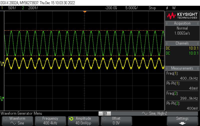
Figure 16: Waveform of the buffer’s input and output of theAM demo signal.The gain is observed to be 1

Figure 17: Aplot of the VTC curve with vDS on the y axis, in V, and vGS on the x axis, in V.The Q point was (6 87, 2 42)

Figure 18: Aplot of iD-vGS curve where iD is on the y axis, in mA, and vGS is on the x axis, in V The Q point was (5 43 ,2 42)

Figure 19: Aplot of iD-vDS curve where iD is on the y axis, in mA, and vDS is on the x axis, in V The Q point was (5 43 ,6 87)
Table 20: Atable consisting of the values that set the Q point for the buffer. Units in in V and mA
(Q-Point) (V)
Gain Cell: TheoreticalAnalysis
(V)


Figure 20: Atheoretical analysis of the gain cell
Amplifiers have three defining characteristics: gain, input resistance, and output resistance
Gain:
Setting the quiescent point is integral to obtaining a required gain Two relationships can aid in this process, the IV and VTC graphs The VTC graph shows what values of VBE and VCE will place the transistor in its three regions, (cut off, active, or saturation), and how much gain to expect The slope of the VTC curve increases as VBE increases and VCE decreases Consequently, obtaining the maximum gain means increasing VBE and decreasing VCE as much as possible without allowing VCE to drop below .3V, the condition for saturation. Furthermore, the slope of the VTC curve is most linear at the center Therefore we predict an optimal Q point is somewhere between and VCE = 3V ������ = 1 2 ������
The same ideas apply for the IV graphs In the case of the Ic vs Vbe graph, even though the relationship is non-linear, there is a region that is linear Maintaining a pair of Ic and Vbe values that remain in that linear section allows the near linear amplification that is desired. It also gives insight to sensitivity in the circuit design; due to their exponential relationship, Ic can be chosen from a wide range of values without affecting Vbe too heavily, upsetting the relationship between Vce and Vbe previously mentioned. But we also must consider that even a small change in Vbe could cause a very large change in Ic, easily bringing the quiescent point out of the linear region and increasing the power consumed
All the same concepts apply to the Ic vs Vce graph but with one useful exception. Rc, using Ohm’s Law, can be found from Vcc, Vce, and Ic By considering the quiescent point on the Ic vs Vce curve, the reciprocal of the slope at that quiescent point can give a value for Rc.
These two graphs show us that the most important characteristics for determining gain are Ic, Vce, and Vbe The resistors’only purpose is to maintain these conditions
Finally, Equation 7 shows that the gain and RC and IC have a direct relationship But the restriction is VCE; if RC were to be very large, a very large voltage would occur across it forcing VCE to be small which might coerce the transistor into saturation VCE can be maintained over .3V by choosing a small enough emitter resistor but, since IE and IC also have a direct relationship, this could also decrease IC and therefore the gain
Input Resistance:
The input resistance of a BJTis the parallel combination of the biasing resistors, (R1 and R2 in Figure ), and the internal resistance named . Since the input resistance will make a �� π voltage divider with the buffer, the larger the input resistance the more of the input voltage will be retained. Since only the ratio of the biasing resistors is relevant for maintaining the desired VBE, scaling both resistors by the same factor is a very simple way to increase the input resistance. Observing Equation 4, we can see that increasing IC decreases which is �� π undesirable for two reasons: first, a larger IC means a larger gain. Second, a smaller means �� π less of the proceeding block’s input voltage is transferred to the gain cell Furthermore, is �� π usually in the tens of ohms so no matter how much the biasing resistors are scaled, the parallel combination will always give a equivalent resistance less than .This is one of the reasons a �� π buffer is required
The largest input resistance is obtained when R1=R2. But since a larger VBE would grant a larger IC, R2 will likely be larger than R1, which will reduce the input resistance A balance between the input resistance and VBE will need to be found in order to optimize the circuit.
Additionally, Equation 11 recommends keeping the base current as low as possible to increase the value of rpi; this is fortuitous since the existence of the base current reduces the collector current, directly reducing the gain and transistor efficiency. Finally, increasing the biasing resistors will also decrease the current that passed through them.This will reduce the power consumed. But there is a limit; if the biasing resistor currents reach µAmagnitudes the gain cell will likely experience more noise than if the magnitudes were mA
Output Resistance:
Since the output resistance will create a voltage divider with whatever block succeeds it, the lowest output resistance is desired.This is beneficial because this also encourages an increase in IC which promotes more gain
According to Equation 3 the output resistance is defined by the transconductance, the internal output resistance, and the collector resistance.As seen in Equation 5, the transconductance has a direct relationship with the collector current and as seen in Equation 6 the internal output resistance has an inverse relationship with the collector current. But since Equation 3 contains the reciprocal of the internal output resistance, increasing the collector current will increase both the internal output resistance as well as the transconductance, ultimately increasing the output resistance. Increasing the collector resistance will also decrease the output resistance which is fortuitous since this also could encourage more gain
Simulation:

Figure 21: The LTspice circuit diagram of the gain cell circuit that contributes to the whole of the LNA Circuit is biased with a two resistor network and is supplied by a 12 25V source as well C1 and C2 are coupling capacitors Circuit is fed with a 30mV peak to peak signal

Figure 22: LTspice LNAtransient analysis input and output waveform 15mV amplitude is amplified to be a 2 26V amplitude This yields a theoretical gain of 150 6 Which is more than our design goal.
Table 21: Atable consisting of the simulated nodal voltages, currents, beta, output and input resistances, and gain.
Design/Measurements:

Figure 23: Realized circuit on breadboard of the LNA’s gain cell with input from the buffer at Vsig1 and Gain cell output VoGC.The transistor used is a 2N3901. R1 and R2 biasing network is realized using a potentiometer The same is done for the collector resistor
Since BJTs naturally produce less noise and a higher gain, (demonstrated by their VTC graph), than MOSFETS a 2N3904 was chosen
The actual value of beta of the 2N3904 was calculated for the theoretical analysis This was done by creating a dummy circuit in LTSpice and on a breadboard, careful to maintain the circuits deep in active mode The resistances and voltages were then fine tuned to be as similar as possible and beta was calculated.
Again, a spreadsheet technique was chosen, implementing the equations featured in Figure 20 The values of VCC, IC, and VCE were given ranges This again allowed the group to
see patterns more efficiently than if computing the theoretical analysis by hand The value of RC was cross-referenced to the chosen Q point on the iC-vCE graph for consistency. Potentiometers were surrogates for fixed resistors so that experimentation was easier
Table 22: Atable consisting of the measured values of the passive components
Table 23: Atable consisting of the measured nodal voltages, currents, beta, output and input resistances, and gain


Figure 25: Waveform of the gain cell’s input and output using theAM demo signal with a realized gain of 148 3

Figure 26: Aplot where vCE is on the y axis, in V, and vBE is on the x axis, in V The Q point was (4.02 ,0.710 ).

Figure 27: Aplot where iC is on the y axis, in mA, and vBE is on the x axis, in V.The Q point was (7 4, 0 710 )

Figure 28: Aplot where iC is on the y axis, in mA, and vCE is on the x axis, in V.The Q point was (7.4 , 4.02).
Table 24: Atable consisting of the values that set the Q point for the gain cell. Units in in V and mA
(V)
4 02 0 710 7 4
Discussion:
(mA)
The biasing resistors for the buffer should have been larger so that more of the band pass’s output could be retained When designing the buffer and gain cell separately the group should have paid more attention to their output and input resistances; when the two were first connected they performed underwhelmingly This led to a redesigning of the buffer that could have been avoided if the resistances were more carefully considered
Mixer:
Once the bandwidth of signals is amplified a down conversion of frequency is required.This is achieved with a diode mixer consisting of a 1N4148.
TheoreticalAnalysis:
The only model available to us for diodes in ac is the small signal model Since the LNAis feeding a signal with an amplitude of 5 7V, that model will not accurately describe the mixer’s behavior.
Instead discussion of the circuit at dc will give enough of an understanding to design the mixer The biasing voltage sets the quiescent point of the diode, which in this case, only needs to guarantee the diode remains forward biased; any excess voltage would just add more power consumption Therefore the biasing voltage is 5V Considering the exponential relationship between the diode voltage and current, the theory predicts that the waveform would have the maximum amplitude when the biasing voltage is close to 5V Instead of adding another dc supply, a potentiometer is used to supply this 5V from the 12 25V dc supply R1 and R2 create a voltage divider with R4 for the oscillator input and LNAinput.This means the smallest R1 and R2 possible gives the largest amplitude In fact, removal of them gives the maximum amplitude
Simulation:
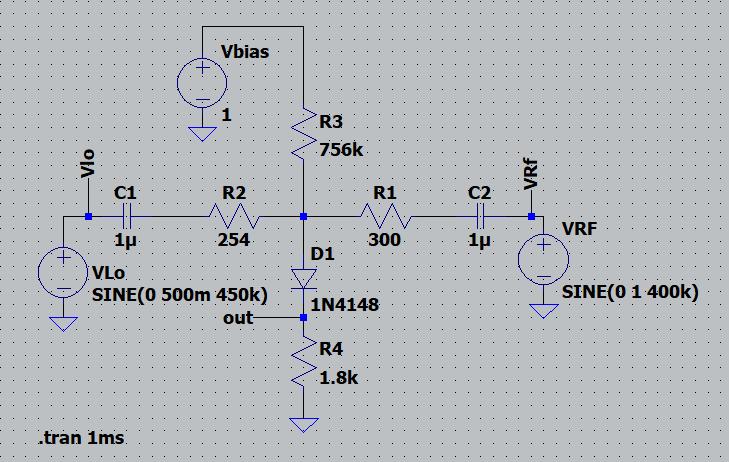
Figure 29: L as two µfarad capacitors and a bias voltage of 1V using a 1N4148 Diode Two signals are mixed, Vlo and VRF
Table 25: Atable consisting of the four simulated resistor values and the biasing voltage


31: LTspice FFTplot in dB Aspike is noticed at 50kHz as desired Mixer amplitude at 50kHz is -27.8dB.

Design/Measurements:

Figure 33: Mixer circuit realized and built on a breadboard. R1, R2, and R4 utilize series resistances C1 would be the coupling capacitor for between the LNAand mixer Vin(LNA) and VLO are the signals being mixed to produce the output VoMXR
Since there were no simulation values to start with we replaced R3 with a potentiometer so different resistances could be tried.The best resistance was found by watching the waveform’s amplitude change as the potentiometer was adjusted, found inTable 26 Any larger values would steadily decrease the amplitude. Interestingly, values around a couple hundred ohm would stop the waveform completely This is likely due to the diode entering cut off This behavior correlates with the guess that placing the quiescent point as close far left as possible on the IV graph would create the largest amplitude.
To confirm that the mixer was handling the frequencies properly, a FFTfunction was utilized on the oscilloscope and can be seen in Figure 35 The R3 resistance was confirmed by watching the 50kHz peak while turning the potentiometer.
It was also discovered that when the potentiometer gave the anode voltage a value of 1.1V, the waveform had a larger amplitude than at cut off.This behavior might be explained by an extreme amount of current running through the diode.The diode should not be operated at such high voltage but it was an interesting correlation
When the LNAsignal’s frequency was modified the spacing between the peaks was changed When the local oscillating frequency was changed the peaks were translated along
the x axis The group was not sure what explained this behavior but felt a little more comfortable with how the mixer multiplied the frequencies.
Removing R1 and R2 did increase the amplitude of the output but appeared to cause more inconsistent behavior in the mixer.The reasons behind the behavior were never found but it is likely due to the changing amplitude that the LNAwould input to the mixer
Theoretically having R1 and R2 equal would be the best configuration but in practice we found the opposite. Since the LNAwas outputting a voltage of 5.7V, which is 4.7V higher than the oscillating frequency, it made sense to have differing values This seemed to increase the amplitude of output voltage The inequality in R1 and R2 also modified the amplitude of the 350kHz, 400kHz, and 450kHz harmonics.
Measured Values:
Table 26: Atable consisting of the four resistor values and the biasing voltage


Figure 35: AFast FourierTransform plot for the mixer, with the amplitude on the y-axis in dB and the frequency, in kHz, on the x-axis The desired peak is at 50kHz The amplitude at 50kHz is -37.5dB and this peak represents the down-converted signal.
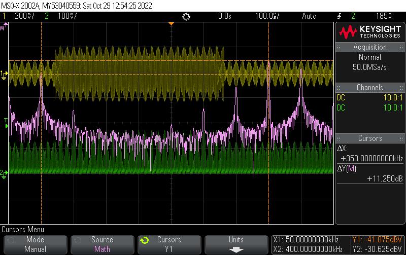
Figure 36: AFast FourierTransform plot for the mixer using theAM demo signal, with the amplitude on the y-axis in dB and the frequency, in kHz, on the x-axis.The desired peak is at 50kHz The amplitude at 50kHz -41 87dB and this peak represents the down-converted signal
Discussion:
The mixer was the most difficult part of this project due to its inconsistent and inefficient nature.The single diode mixer has poor isolation which spreads its mixing behavior to the LNA, reducing the frequency to about 410kHz. When the group attempted to measure the diode voltage with a multimeter the amplitudes in the frequency response would change We found it difficult to troubleshoot the circuit. In hindsight the inconsistent behavior was a clear indicator to have an active low pass filter to compensate for the erratic behavior It is clear that a Gilbert multiplier may well be worth the time
Low Pass Filter:
The mixer naturally produces two sets of modified signals, one with higher frequencies and one with lower Since the desired signals are the down converted, a low pass filter is needed to attenuate the higher frequency group.This was achieved with a second order passive filter.
TheoreticalAnalysis:

Figure 37: Atheoretical analysis for a second order passive low pass filter Q, R, C and the transfer function are found and are used to design a filter for the project Amore elaborate explanation is provided below.
First, the circuit variables are converted from the time domain to the frequency domain, in terms of s.The inductor and capacitor are combined in parallel to create Z2. Using the voltage division equation and solving for Vo(s)/Vi(s), the transfer function is found
Since the receiver will operate in theAM range, the required bandwidth is 8kHz. If the expected center signal is 50kHz then the cut off frequency 54kHz.The cut off frequency is dictated by the inductance and capacitance of the circuit Since the only inductor the group has access to is 100mH, the required capacitance can be found using Equation LP2. Since the max frequency is 50kHz, Equation LP4 can be used to find the quality factor This equation was found in Figure 17 16 on page 1313 of the textbook Using Equation LP3 with the quality factor the required resistance can be found.
Table 27: Atable consisting of the calculated values of the inductor, capacitors, and resistor used in the breadboard circuit.The units are µH, nF, and kr.
Simulation:

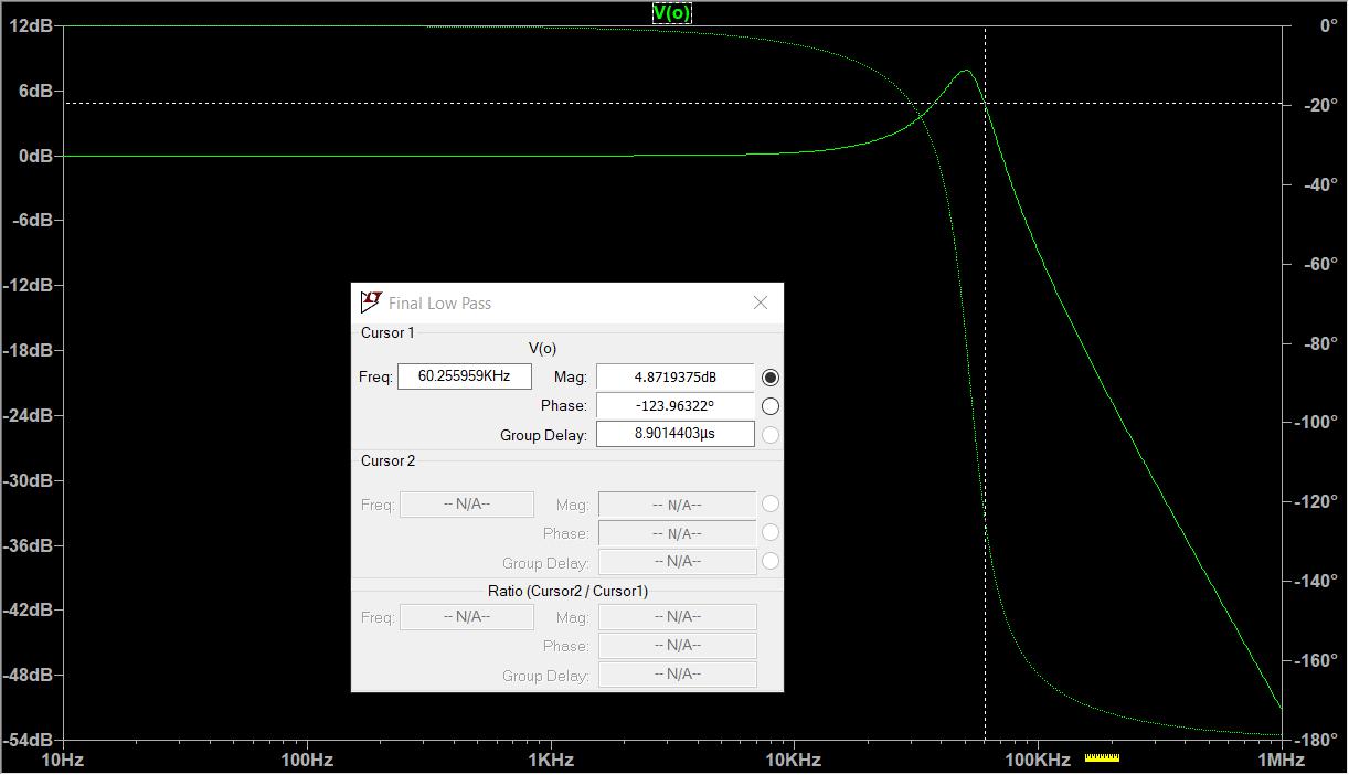
Figure 39: LTspice ac analysis for the above lowpass filter Corner frequency of 60kHz
Table 28:Atable consisting of the simulated values for the capacitance, resistance, and inductance
Inductor ( H)µ
(nF)
(k )Ω 100 01 92 0080
Design/Measurements:

Figure 40: Realized circuit build of the passive lowpass filter built on a breadboard C1 utilized parallel capacitance. VoLPis the low-pass output and VinLPis the input to the filter from the output of the mixer
Table 29: Atable consisting of the measured values of the inductor, capacitors, and resistor used in the breadboard circuit.The units are µH, nF, and kr.
Table 30: Atable consisting of the measured values for the corner frequencies as well as the voltage ratio, in kHz.

Figure 41: Afrequency response plot with gain, in dB, on the y-axis and frequency logarithmically on the x-axis, in kHz
Unsatisfied with the corner frequency, different resistances were tried in an attempt to modify the selectivity We determined the gain and bandwidth have an inverse relationship, confirming the gain-bandwidth product. Since the starting signal is 30mV the loss of output voltage was a major concern and the group decided to sacrifice some precision to maintain as much gain as
possible The original configuration was the best of both worlds The alternate values can be found inTable .
Table 31: Alternate resistance values for the low pass filter and their resulting bandwidths and gains, in , kHz, and dB Ω
Discussion:
The corner frequency is not correct but this is very likely due to the imprecise capacitors. Since the corner frequency is very sensitive to changes in capacitance, the 90 74nF capacitor likely caused the undesirable shift in the corner frequency.
Stacking multiple second order filters, depending on the mixer, had better effects than just one second order filter Just like the band pass, the implementation of higher order filters would have been well worth the effort.
Complete Implementation:

Figure 42: Realized circuit of the first five stages to theAM-receiver Input is at the band-pass filter, output is at the Low-pass filter. Orange jumper cables indicate linked blocks, red is positive supply, black is ground VLO is another input fed to the mixer


Figure 44: The output waveform and FFTof the entire circuit.The first cursor is at 50kHz and represents the peak while the second cursor is at 400kHz The span was set at 500kHz with a center of 250kHz.The difference in amplitudes was 23.125dB

Figure 45: Aclearer resolution of the output waveform. The frequency of the output is 50kHz, and the amplitude is 35mV peak-to-peak The span was set at 500kHz with a center of 250kHz
Discussion:
The team prioritized simplicity We figured if each block was as simple as possible then when it came time to connect them all the circuit would be easy to troubleshoot and manage. This resulted in using only second order passive filters and the diode mixer instead of the Gilbert mixer Additionally, we optimized each block in isolation without much consideration of how they would behave with each other. Some examples follow: with the exception of the LNA, input and output resistances were not considered at all We did not consider adapting the input resistance for the mixer to balance the 5.7V signal the LNAproduced. We did not consider how inconsistent the diode mixer would be due to its simplicity and also did not build an active low pass filter to compensate for the mixer’s 193mV output The goal of simplicity was achieved but the trade off with reliability is not a reasonable one. We learned to not build in a vacuum.
Using potentiometers was good for experimenting but replacing them with set resistors makes much more sense for stability; when transiting the board or rearranging components the potentiometers would slightly change and would need recalibration.
We also learned the value of consulting others Whether they could tell us which paths were fruitless or could give a new perspective on an issue, sharing information and experience accelerated progress.This is amplified further due to our lack of experience with the equipment and circuit behavior
Conclusion:
The group learned abundantly. We learned how to design filters, amplifiers, and mixers for a set of parameters Unlike theoretical analysis problems, the group experienced and struggled with trade offs in, not only balances between variables, but also holistic design like power consumption, simplicity, reliability, and performance.
We also learned how to work as a team more effectively We learned how to play to each other’s strengths, adapt our communication and design behaviors, and gain more comfort with our limits
BEGIN REPORT PART II:
Abstract:
The project consists of designing anAM receiver via theoretical analyses, LTSpice, and breadboard prototyping Asecond order passive bandpass filter, a BS170 common source used as a buffer, a 2N3904 common emitter used as an amplifier, a single 1N4148 diode mixer, second order active and first order low pass filters, a second LNA, a peak detector with a 1N34, and finally anAB amplifier with 2N3904s and a 2N3906 were the chosen components The final circuit was able to create a square wave with a fundamental frequency of theAM signal’s modulation but was unable to level the top of the waveform due to higher frequencies not effectively being filtered
Introduction:
The task involved creating a circuit whose output was a square wave with a fundamental frequency the same as theAM signal’s modulation The components used were ceramic and electrolytic capacitors, molded inductors, a BS170, a 2N3904, a 1N4148, potentiometers, a 1N34, a OP27, BS880 breadboards, dc power supply, and twoAgilent two channel oscilloscopes.

Colpitts Oscillator Values:
Table 32: Component values for the oscillator simulation
Ω
Table 33: Node voltages, currents and circuit characteristics for the oscillator simulation.
Table 34: Measured values for the realized breadboard build for the colpitts oscillator
Table 35: Measured node voltages, currents and transistor characteristics of the realized colpitts oscillator
Active Lowpass Values:
Table 36: Simulation component values for the simulation diagram above.
Table 37: Simulated circuit characteristics of the active lowpass filter.
Table 38: Measured component values and bias voltage from the realized circuit above.
Table 39: Measured circuit characteristics of the active lowpass filter
Peak Detector Values:
Table 40: Simulation component values and time constant
Table 41: Measured component values and time constant for the realized peak detector
ABAmplifier Values:
Table 42: Q1 simulation voltages, currents and circuit characteristics
Table 43: Q2 simulation voltages, currents and circuit characteristics
Table 44: Q3 simulation voltages, currents and circuit characteristics.
Table 45: Simulation component values
Table 46: Q1 measured voltages, currents and circuit characteristics
Table 47: Q2 measured voltages, currents and circuit characteristics
Table 48: Q3 measured voltages, currents and circuit characteristics.
Table 49: Measured component values for the realized AB class amplifier.
Table 50: Calculated power results forAB class amplifier
Colpitts Oscillator:
TheoreticalAnalysis:

Figure 46: Atheoretical analysis of the Colpitts oscillator using the small signal model The transfer function, resonance frequency equation, and the gain requirement are found.
There are two sections in an oscillator: the amplifying section and the frequency selective network Both sections are connected in a positive feedback configuration; positive feedback means that the outputs of each section are added to the inputs of the others More specifically, the thermally generated noise is amplified by the amplifying section and is fed into the FSN The FSN, by nature, allows only certain frequencies to the output which are then fed back into the amplifying section These frequencies are then again amplified and any newly and undesired frequencies are again attenuated in the FSN This process repeats until a set of frequencies have significant amplitude This “encouragement” between the two sections is only possible because of positive feedback
The Barkhausen criterion states that the product of the ratios of the output to the input voltage of both the amplifying section and FSN must be greater or equal to one for consistent oscillations to occur The ratio for the amplifying section is called gain while the ratio for the FSN is called the feedback ratio sometimes denoted as Intuitively, the Barkhausen criterion states β that the combined effort of the two sections must be large enough to cause an increasing positive net energy supply; otherwise a negative net energy supply will occur and the energy for the oscillation will decrease into nothingness
The frequency selective network consists of two capacitors and an inductor These two capacitors act as a voltage divider; C1 controls the output voltage while C2 provides the positive feedback Since the capacitors have to “share” the voltage output from the amplifying section they define the feedback ratio The inductor creates a tank circuit with the two capacitors, allowing oscillations to occur from the dc power supply
Simulation:

Figure 47: LTspice simulation diagram for the Colpitts oscillator using an npn transistor, a frequency selective network and RF choke The values in the simulation diagram may not reflect the final realized circuit

Figure 48: Colpitts oscillator output with a peak-to-peak voltage of about 21V.

Figure 49: Colpitts oscillator simulation FFTplot for the above circuit diagram Oscillation frequency of 399.22kHz
Table 51: Component values for the oscillator simulation.
Table 52: Node voltages, currents and circuit characteristics for the oscillator simulation
Design/Measurements:

Figure 50: Realized breadboard circuit of the 2N9304 transistor colpitts oscillator The output voltage is stepped down to be 1Vpp after the variable resistor next to C5 Series inductance was used for L1 and L2.
Table 53: Measured values for the realized breadboard build for the colpitts oscillator.
Table 54: Measured node voltages, currents and transistor characteristics of the realized colpitts oscillator.
The first attempt at the Colpitts oscillator was with a LM741 op amp.This model was unable to achieve the desired oscillation frequency of 400kHz The issue with the circuit was most likely from the op amps gain-bandwidth product limitation For this reason the group attempted to use an OP27 due to its 8MHz gain bandwidth product, but the circuit still didn't work as desired After experimentation with different capacitors as well as a different positive feedback resistors, the group then tried a 2N3904 transistor oscillator, since information on such a circuit was much more abundant than the op amp configuration.
Instead of trying to obtain 400kHz by measuring every capacitor with an impedance analyzer, the group decreased the biasing voltage knowing the frequency had an inverse relationship Not only was this a fast fix to the frequency inaccuracy but it also decreased the amount of power used by the oscillator Avoltage divider was used to reduce the oscillator’s output to 1V peak to peak.The group ultimately prioritized attaining the 400kHz requirement since the voltage could be so easily stepped down to what we wanted
An inductor with an inductance of 100µH was originally chosen to be the RF choke because the team knew that a large inductor was needed. Unfortunately this inductor was not large enough and sent a 400kHz voltage throughout the rest of the receiver Six 20mH were then used instead which successfully blocked the 400kHz voltage from bleeding to the rest of the circuit but also modified the impedance for Rc.The group then had to modify the resistors and FSN as well as the biasing voltage until 400kHz was again generated


Assessment:
Instead of using a voltage divider at the output of the oscillator, a much better design choice would be modifying the loop gain variables to produce a natural output of 1V This would require reducing the 2N3904’s gain which likely would require a change in the reactance values of the FSN to maintain the Barkhausen criterion. It is not clear if the group even possessed capacitors or conductors that could satisfy those conditions
At first the feedback factor being so large worried the team. But if the feedback factor was larger than the gain of the transistor could be smaller This probably made the circuit consume less power
Utilizing the op amp configuration would have made reducing the gain easier but would have also required a negative power supply lead The op amp also had a gain bandwidth product to mind as well as offset reduction
Active Low Pass Filter: TheoreticalAnalysis:


Figure 54: Active lowpass filter simulation diagram, V+ = 12.25V and V- = -12.25V biases an OP27 opamp.

55: Frequency response of the active
circuit diagram above.
55: Simulation component values for the simulation diagram above
Table 56: Simulated circuit characteristics of the active lowpass filter.
Design/Measurements:

Figure 56: Realized circuit of the active lowpass filter with an OP27 opamp, cascading into our redesigned passive lowpass filter C1 and C2 utilize parallel capacitance
Table 57: Measured component values and bias voltage from the realized circuit above
Even though the cascade of passive low pass filters was enough to gain a 20dB difference between the frequency peaks the output waveform had a peak-to-peak voltage in the 10s of mV Originally an active low pass filter was avoided due to increased complexity and power usage but the activation voltage required for 1N34 made an active filter a necessity
Anew challenge that opamp filters present that is absent with passive filters is the gain bandwidth product Fortunately since the allowable frequencies were all low, (around 60kHz), a notable gain could be achieved without encountering limits Furthermore, the opamp used was a OP27 which has a gain bandwidth product of 8Mhz, eight times greater than the LM741; this is such a large gain bandwidth product that it almost becomes negligible in the design At first the filter was given a gain of approximately 2.5 but it was lowered to because it preceded the second LNA. Since the LNAwas designed for an input of 30mV, the filter needed an output in that range Upon experimentation it was discovered that the maximum input that would consistently not cause clipping in the second LNAwas approximately 45mV.The team decided to design the filter’s output to around 45mV, (instead of the predicted 30mV), due to the large peak-to-peak voltage drop across the peak detector
With just the second order active low pass filter the 20dB gap was not reached.An additional passive low pass filter was attached to the output because the design for a third order active low pass filter is far more involved than a second order

Figure 57 : Active Low pass filters input and output waveforms at the corner frequency of about 57kHz The top waveform is the 1V input, and the bottom wave is the output
Table 58: Measured circuit characteristics of the active lowpass filter
Corner Frequency (kHz) Quality Factor Gain (at fo)

Figure 58: Frequency response plot of the realized active low-pass filter with the corner frequency of about 56kHz Input and output data was gathered for different frequencies and plotted.
Assessment:
Even though the active low pass filter consumed more power, complicated the circuit, and took longer to design, the benefits outweighed the detriments
The team was not aware of how much larger the OP27’s gain bandwidth product was than the LM741’s.This larger gain bandwidth product could have allowed a greater amplitude that, in tandem with an increased gain in theAB amplifier, could have made the second LNA negligible.
With more time developing a third or even fourth order active low pass filter would have been a better choice considering the single passive low pass filter reduced the output by approximately 20mV.
Second LNA:
Since the peak detector’s output voltage was 10 times less than the input voltage, a second LNAsucceeded the low pass filter and proceeded the peak detector.This LNAwas a copy of the first LNA


Figure 60: Second LNA input and output waves Gain of 144 82 Peak Detector:
TheoreticalAnalysis:
PD1)
= ����
The purpose of the peak detector is to supply a constant output voltage whose value is that of the peak of the input voltage This is accomplished with a diode and capacitor; a capacitor’s voltage, (assuming a matched frequency and time constant), will follow the sinusoidal input voltage. If a diode is placed between the input voltage and the capacitor, then the capacitor will be charged for only half the cycle, not discharging during the other half In theory, once the capacitor is fully charged, (to either negative or positive peak voltage), it will retain the charge indefinitely and achieve the purpose of a peak detector This model is impractical
Amore practical model, shown in Figure , includes a resistor in parallel with the capacitor With the resistor the capacitor now discharges to 36 8% of its maximum voltage during the interval of its time constant Since an ideal peak detector creates a constant output voltage, the time constant must be much greater than the period of the input voltage. In this case, the resistor that determines the time constant for the peak detector in the input resistance of theAB amplifier.
Simulation:
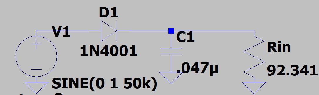
61: LTspice simulation diagram of the peak detector with a 1N4001 diode.

Figure 62: Simulation input and output of the peak detector.
Table 59: Simulation component values and time constant.
Ω
Design/Measurements:

Figure 63: Realized circuit of the peak detector Vi is the input to theABclass amplifier
Table 60: Measured component values and time constant for the realized peak detector
Since the input resistance of theAB amplifier is the resistor that defines the peak detector’s time constant it is far more convenient to manipulate the time constant via the capacitor.

Figure 64: Peak detector input and output waveforms The output resembles that in the simulation In order to have a reasonable output, the group needed to have a high input of about 4.5V
Assessment:
The success with the active low pass filter was foreshadowing for the peak detector; unfortunately the group missed this foreshadowing An active peak detector would have eliminated the need for the second LNAand potentially the active low pass filter.This also would have made troubleshooting easier because the peak detector’s output needed to be amplified by theAB amplifier to have a large enough peak-to-peak voltage to be clearly visible on the oscilloscope.
ABAmplifier:
TheoreticalAnalysis:

The basic idea of anAB amplifier is to use, (in this case), a npn and pnp transistor to share the responsibility of producing an output voltage. Since current in pnp transistors flows in the opposite direction of a npn, the npn transistor creates the positive half cycle of the output voltage while the pnp creates the negative half cycle of the output voltage Since transistors have a limited range of operating voltages that cause a linear output, allowing each transistor to create only half the peak-to-peak voltage allows a great output voltage in comparison to anA amplifier that creates the entire peak-to-peak output voltage in its linear range.
Technically the circuit described is a B amplifier B amplifiers suffer from a phenomenon coined crossover distortion that occurs when the input voltage is insufficient to produce the required voltage across either of the transistors’emitter and base junctions. Since neither transistor is conducting in this region the output signal is 0 volts This is fixed by changing the conduction angle of each transistor from pi to some other angle This is achieved by placing diodes across the base and emitter junctions of the npn and pnp transistors to force at least a
voltage of 6V across the base and emitter junctions This changes the conduction angle of both transistors and avoids crossover distortion.
The third transistor Q1 is a gain cell similar to the component created in the LNAsection
Simulation:

Figure 66: LTspice simulation diagram of theABclass amplifier using three transistors, two npn and one pnp.The amplifier has a VCC of 12.25V.

Table 61: Q1 simulation voltages, currents and circuit characteristics
Table 62: Q2 simulation voltages, currents and circuit characteristics
Table 63: Q3 simulation voltages, currents and circuit characteristics.
Table 64: Simulation component values.
Design/Measurements:

Figure 68: The realized circuit of theAB class amplifier connected the peak detector Q1 and Q3 are the npn transistors and Q2 is pnp.

Figure 69: VTC of the Q1 transistor in theAB class amplifier.
Table 65: Q1 measured voltages, currents and circuit characteristics.

70: VTC of the Q2 transistor in theAB class amplifier
Table 66: Q2 measured voltages, currents and circuit characteristics.

Figure 71: VTC of the Q3 transistor in theAB class amplifier
Table 67: Q3 measured voltages, currents and circuit characteristics.
Table 68: Measured component values for the realized AB class amplifier
Table 69: Calculated power results forAB class amplifier
Assessment:
TheAB amplifier performed as expected and had no issues. In hindsight the second LNApossibly could have been avoided if the gain of the active low pass filter andAB amplifier were both increased.

