


Renesas Electronics Corporation has introduced the Lithium-Ion Battery Management Platform, an all-in-one solution for managing lithium-ion battery packs in a wide range of batterypowered consumer products, such as ebikes, vacuum cleaners, robotics, and drones. With pre-validated firmware provided, the R-BMS F (Ready Battery Management System with Fixed Firmware) will significantly reduce the learning curve for developers, enabling rapid designs of safe, power-efficient battery management systems.
Designed for lithium-ion batteries in both 2-4 and 3-10 cell series (S), the LithiumIon Battery Management Platform (R-BMS F) include Renesas’ industry-leading fuel gauge ICs (FGICs), an integrated microcontroller (MCU) and an analog battery front end, pre-programmed firmware, software, development tools and full documentation – all available in complete evaluation kits that are now ready to ship.
Firmware is essential in battery management systems as it is used to monitor batteries’ state of charge (SoC), state of health (SoH), current, and temperature, as well as actively balancing the voltages of the individual cells, and detect faults. In some cases, however, consumer electronics developers may lack the highly specialized expertise needed to develop control algorithms that keep the batteries operating in a safe temperature region and ensure adequate battery life over many charge/discharge cycles.


The Renesas’ Lithium-Ion Battery Management Platform includes built-in, pre-tested firmware designed to work with the FGIC’s on-board MCU. The firmware includes critical pre-programmed functions to maximize battery life and ensure safe operation. These include cell balancing, current control, and voltage and temperature monitoring.
For added flexibility, the battery management system lets developers set many parameters to meet specific requirements and adjust the solution for different cell chemistries via a graphical user interface (GUI), without the need for a full integrated development environment (IDE).
Both R-BMS F solutions contain a full evaluation kit, which has all the hardware, software, tools and documentation required to start developing. The underlying hardware powering the R-BMS F is Renesas’ FGIC solution, which combines an analog battery front end and an ultralow-power RL78 MCU into a single, small package. The analog portion provides accurate measurements of cell voltage, current and temperature, as well as controlling the external MOSFETs and converting analog data to digital signals.
The digital section is where synchronous functions reside, including the main CPU, clocks, timers and serial interfaces. Also included in the evaluation kits are: preprogrammed firmware stored in embedded flash memory with the flexibility to set


the battery pack and cell chemistry parameters; the USB System Management Bus (SMBus) interface; GUI-based software; cables to communicate with the host system; dedicated development tools for parameter setting; and full documentation, including schematics and an engineering bill of materials (eBOM).
With these resources, developers can confidently innovate intelligent power management systems that safely monitor battery usage and provide longevity, while reducing their impact on the environment. Renesas plans to include turn-key RBMS F solutions in all future FGICs.
2-4 Cell Series Solution
(RTK0EF0163DK0002BU)
The R-BMS F for 2 to 4S cell (~8V to 16V) solutions targets small vacuum cleaners, robotic vacuums, consumer and medical devices and runs on Renesas’ RAJ240055 Li-ion battery FGIC. Renesas offers Smart Robot Vacuum Cleaner | Renesas by combining this FGIC with other devices from its portfolio.
3-10 Cell Series Solution
(RTK0EF0136DK0002BU)
The R-BMS F for 3 to 10S cell (~12V to 40V) solutions runs on Renesas RAJ240100 and RAJ240090 Li-ion battery FGICs, with target applications including e-bikes, emobility, vacuum cleaners, robotics, drones and industrial, consumer and medical systems.
Renesas Electronics Corporation www.renesas.com
integrated gate driver photocoupler from Toshiba enhances safety when switching SiC MOSFETs in


Renesas Extends Mid-Class AI Processor Line-Up with RZ/V2N MPU Integrating DRP-AI Accelerator for Smart Factories


Management
Advertisement
Web

Contributing


Unveils 2000V High-Voltage Rectifiers with Improved Efficiency and Enhanced Thermal Performance
WeEn Semiconductors, a leader in advanced bipolar power semiconductor solutions, announced the launch of its 2000V High-Voltage (HV) series of standard rectifiers. Designed to address the evolving demands of high-voltage systems, these rectifiers achieve a 5% reduction in forward voltage drop (VF) and a 20% improvement in thermal resistance compared to competing solutions. The innovations enable significant efficiency gains, lower cooling costs and extended operational lifespans in renewable energy storage and electric vehicle (EV) fast-charging applications.
Key Features and Benefits
The 2000V HV series integrates a proprietary single-chip design to minimize conduction losses with an optimized ORing circuit that enhances thermal management. This combination ensures reliable performance in 1500V bus systems and 1000VDC EV charging infrastructure, where voltage spikes and stray inductance pose risks to component longevity. Additional advantages include:
• High Junction Temperature (Tjmax): Operates up to 150°C, ensuring stability in demanding environments.
• Superior Surge Current (IFSM) Tolerance : Enhances robustness under dynamic load conditions.
• TO247-2L Packaging: Streamlines integration into highpower designs.
Two initial variants are available: the 60A-rated WND60P20W and the 90A-rated WND90P20W. These devices are engineered to mitigate voltage spikes in fast-changing EV charging loads, safeguarding systems against failure while improving power density.
The 2000V HV rectifiers are now available globally in TO2472L packages. Target applications include solar PV inverter and storage systems, DC fast EV chargers, and industrial power systems requiring high voltage endurance and reliability.
■ WeEn Semiconductors | www.ween-semi.com

NOVOSENSE Microelectronics, a semiconductor company specializing in high-performance analog and mixedsignal chips, has announced the European launch of four new industry-leading interference-resistant CAN transceivers and a stepper motor driver to add to its portfolio of automotive body control devices for European OEMs and Tier 1 suppliers.
As the number of electronic control units (ECUs) in vehicles continues to grow, in-vehicle communication must be more robust and reliable than ever. CAN networks serve as the communication backbone for systems such as lighting, ignition devices, powertrain, inverters, and other essential body electronics. However, electromagnetic interference from powertrain systems, ignition devices, inverters, and wireless equipment can disrupt CAN communication, leading to signal errors or system failures. The NOVOSENSE CAN transceivers have successfully passed the stringent requirements of IBEE/FTZ-Zwickau electromagnetic compatibility (EMC) certification, which is based on IEC62228-3 and referenced by automakers within Europe and beyond.
NOVOSENSE will be showcasing the full range of automotive body control products below at PCIM Europe 2025 in Nuremberg, Germany, from May 6-8 at Hall 4A, Booth 119.

• NCA1044-Q1 very low-current standby mode with BUS wake-up capability, offers excellent EMC performance and proprietary ringing suppression for energy-efficient ECU operation. Supports CAN FD communication up to 5 Mbps.
• NCA1057-Q1 supports silent mode offers excellent EMC performance and proprietary ringing suppression for energyefficient ECU. It also includes thermal protection and dominant timeout for enhanced system safety and reliability.
• NCA1043B-Q1 Low-power management controls the power supply throughout the node while supporting local and remote wake-up with wake-up source recognition.
• NCA1145B-Q1 offers low power consumption in standby and sleep modes and supports CAN partial networking using ISO11898-2:2024 compliant selective wake-up functionality. It features excellent EMC performance and proprietary ringing suppression function.
• NCA1462-Q1 is a high-speed CAN FD transceiver with signal improvement capability (CiA601-4 standard), supporting up to 8 Mbps. It reduces signal ringing in large topologies, ensures tight bit timing symmetry, and offers seamless replacement for standard CAN and CAN FD transceivers.
High-side switch series
NSE34/35xxx is designed to drive resistive, inductive, halogen, and capacitive loads in automotive BCMs and ZCUs.
Available in 1-, 2-, or 4-channel variants in HSSOP-14/16 packages with Rds(on) from 8 to 140 mΩ, the series offers precise current sensing for diagnostics and monitoring, integrated protection features, and AEC-Q100-012 Grade A certification for over one million protection cycles.
Bipolar stepper motor driver
NSD8381-Q1 with built-in current control, sensorless stall detection, and full-featured diagnostics. It supports up to 1/32 microstepping, operates up to 40 V, and delivers up to 1.35 A per channel.
Request a sample application by clicking here.
■ NOVOSENSE Microelectronics | www.novosns.com


Highly integrated gate driver photocoupler
Toshiba Electronics Europe GmbH has launched a gate driver photocoupler (TLP5814H) suitable for driving silicon carbide (SiC) MOSFETs in industrial equipment like industrial inverters, uninterruptible power supplies (UPS), and photovoltaic (PV) inverters, which experience harsh thermal environments. The TLP5814H is a highly integrated gate driver featuring a built-in active Miller clamp circuit that helps improve system safety and lower overall solution size by minimising the number of additional external components required.
The integrated active Miller clamp circuit in the TLP5814H has a channel resistance of 0.69Ω (typ.) and a peak clamp sink current rating of 6.8A. These features help to prevent the selfturn-on phenomenon associated with some power devices like SiC MOSFETs and insulated gate bipolar transistors (IGBTs) which are highly sensitive to changes in gate voltage. The integrated Miller clamp in the TLP5814H reduces system cost, size and complexity by mitigating the requirement for designers to include an additional negative power supply and implement an external active Miller Clamp circuit.
This gate driver photocoupler can provide a maximum peak output current of +6.8/-4.8A with rail-to-rail output, which helps to improve system switching performance while ensuring stable operation. An internal Faraday shield ensures common-mode transient immunity of ±70kV/μs (min).
TLP5814H can operate reliably in temperatures ranging from -40 to 125°C due to the enhanced optical output of the infrared light emitting diode (LED) on the input side and an optimised high-gain, high-speed light-detecting photodiode array, which helps to improve optical coupling efficiency. To improve board layout flexibility, the TLP5814H is offered in a small SO8L package measuring only 5.85 × 10 × 2.1mm. Furthermore, it has a minimum creepage distance of 8.0mm which makes it suitable for use in applications requiring high insulation performance.
Learn more about the TLP5814H gate driver photocoupler on Toshiba’s website: https://toshiba.semicon-storage.com/ eu/semiconductor/product/isolators-solid-state-relays/ detail.TLP5814H.html
■ Toshiba Electronics | https://toshiba.semicon-storage.com

Würth Elektronik is excited to announce the launch of the SN6507 Development Kit [756507], featuring the Texas Instruments (TI) SN6507EVM. This comprehensive solution is designed to help engineers evaluate the performance of TI’s SN6507 transformer driver for isolated power supplies, featuring Würth Elektronik’s WE-PPTI transformer line. The development kit includes two versatile boards and 16 transformer samples, offering unparalleled flexibility for various industrial and medical applications.
The SN6507 Development kit is equipped with a fixed board [650796] offering 24Vin-15Vout configuration, optimized with the WE-PPTI transformer [750319696] for a streamlined design.
The SN6507 Development Kit also includes a configurable board [650700] which enables engineers to evaluate different transformers and specifications to meet diverse application needs. To top it off, the SN6507 kit includes 16 transformer samples, which provide flexibility and customization options during development.
This kit is tailored for applications such as motor drives, isolated power supplies for communication protocols (CAN, RS485, RS-422, RS-232, SPI, I2C), medical instruments, solar inverters, and automation systems. With full EMI compliance to CISPR32 standards, the boards deliver optimal performance in demanding industrial and medical environments, ensuring reliability and efficiency. The fixed and configurable designs allow engineers to adapt and innovate for a wide range of use cases, making the kit an essential tool for design and testing.
Engineers and developers can take advantage of this all-inone solution to simplify their evaluation processes and accelerate their project timelines. The Kit is now available for purchase on the Würth Elektronik website: https://www.weonline.com/en/components/products/DESIGN_KIT_756507
■ Würth Elektronik eiSos | www.we-online.com

The electric two-wheeler market is transforming the transportation industry as consumers embrace e-scooters and e-bikes for both recreational use and daily commuting. Microchip Technology (Nasdaq: MCHP) today announces the launch of its Electric Two-Wheeler (E2W) ecosystem, a comprehensive suite of pre-validated reference designs that addresses key challenges in e-scooter and e-bike development, including power efficiency, system integration, safety and time-to-market. By offering automotive-grade, scalable solutions, Microchip enables manufacturers to streamline development and build reliable, feature-rich electric two-wheelers. Microchip’s automotive-grade components and modular reference designs provide a flexible, scalable platform that adapts to various power levels and feature requirements. Backed by comprehensive design files, schematics, Bill of Materials (BOM), and global technical support, developers can quickly bring next-generation e-scooters and e-bikes to market with optimized power, safety and intelligence.
Optimized Power and Battery Efficiency
• Advanced Battery Management System (BMS) with intelligent power conversion and sensing maximizes energy utilization to extend battery life and vehicle range, as well as increases safety.


Nexperia now offers automotive planar Schottky diodes in space-saving CFP2-HP packaging
• 48V to 12V Power Conversion Reference Design ensures high-efficiency power distribution, improving overall system reliability.
Fast and Flexible Charging Solutions
• 4 kW Single-Phase AC EV Charger Reference Design offers reliable home charging with built-in protection features.
• USB-PD Dual Charging Port is designed to provide fast, flexible charging for mobile devices to enhance user convenience.
High-Performance Traction Motor Control
• 350W to 10 kW traction motor control reference designs deliver smooth acceleration, improved energy efficiency and precise control.
• Pre-integrated firmware and modular design simplify system development and reduces time-to-market.
Seamless System Integration and Smart Vehicle Control
• Vehicle Control Unit (VCU), Remote Keyless Entry (RKE), Hands-On/Off Detection and Acoustic Vehicle Alerting System (AVAS) work together to enhance the security and safety of the electric two-wheeler.
• Integrated telematics and asset tracking provide real-time monitoring, theft prevention and fleet management capabilities.
Intelligent Touch Display and Connected User Experience
• 720×720 round LCD Instrument Cluster using Microchip’s SAM9X75 MPU with MIPI® DSI, dual GbE and NAND Flash offers real-time data visualization and smart connectivity.
• maXTouch® ATMXT640UD and ATMXT641TD touchscreen controllers offers accurate touch performance in extreme weather and rain with thick gloves.
• Cloud-enabled remote diagnostics and performance tracking enhance the rider experience and optimize fleet operations.
■ Microchip Technology | www.microchip.com
Nexperia announced that it is now offering a portfolio of 16 new low VF optimized planar Schottky diodes in CFP2HP packaging. The portfolio includes eight industrial (e.g. PMEG6010EXD), as well as eight AEC-Q101 qualified (e.g. PMEG4010EXD-Q) products. This release supports the growing trend for manufacturers to replace devices in SMA/B/C type packaging with smaller footprint CFP-packaged devices, especially in automotive applications. These diodes are suitable for use in, for example, DC-DC conversion, freewheeling, reverse polarity protection and OR-ing applications.
For maximum design flexibility, this portfolio extension offers reverse voltages VR(max) ranging from 20 V to 60 V and forward currents IF(average) of 1 A and 2 A. The exposed heatsink of the CFP2-HP enables the highest level of heat dissipation (Ptot) at a small package footprint. The CFP2-HP package dimensions are 2.65 mm x 1.3 mm x 0.68 mm (inc. leads).
Utilizing the copper clip design, these packages meet the challenging demands of efficient and space-saving designs. Today, CFP packaging is used by different power diode technologies such as Nexperia’s Schottky and Recovery Rectifier Diodes and will also be extended to bipolar transistors soon. It offers significant product diversity. This further solidifies Nexperia’s position as a leader in packaging innovation, offering customers the widest range of device options from a semiconductor manufacturer with a trusted supply chain.
A low IR optimized portfolio of planar Schottky diodes for automotive and industrial applications will be released in May. To learn more about Nexperia’s planar Schottky diodes in CFP2-HP packaging visit: www.nexperia.com/cfp
■ Nexperia | www.nexperia.com


Author: Rolf Horn, Applications Engineer

The two main types of power-quality problems arising from within equipment are noise and harmonic disturbances.
Electrical noise in electrical power refers to high-frequency voltage variations. High frequency is relative – but always indicates frequencies considerably higher than the system ac frequency. Viewed in the time domain, an ac current should appear as a smooth sinusoidal wave. Noise makes the wave ragged and rough. There is always some noise in the electrical supplies of machinery caused by the resistance of the conducting wires involved. Such noise is called thermal noise and is generally a negligible disturbance. More significant and potentially detrimental noise is that caused by local loads such as welders and electric motors.
As covered in a previous Digi-Key article on the specifics of dirty utility power, there are half a dozen power-quality issues (including voltage surges, outages, frequency instabilities, and noise) that can arise from fluctuations in the local utility power grid. Further complicating matters is that variations can also originate from within each piece of electrically powered automation equipment. Fortunately, components abound to address such electric-power consistency issues. These power supplies and other power components make machinery perform its best and prevent machinery from having a negative impact on the local utility power grid.
Noise from such components and systems can often be difficult to quantify –and pose the most risk of causing affected equipment subcomponents to overheat, wear, and even fail.
Electrical harmonics are voltage or current disturbances at frequencies that are integer multiples of the system ac frequency. They are caused by nonlinear loads such as rectifiers, computer power supplies, fluorescent lighting, and certain types of variable-speed electric motors. Current harmonics tend to be larger than voltage harmonics and actually tend to drive the latter.
These electrical harmonics (due to the way they induce heat generation) can dramatically degrade the efficiency and life of electric motors.
They may also cause vibrations and torque pulsations in the mechanical output of electric motors ... which shortens the life of the power-transmission subcomponents integrated into the motors – especially the shaft-supporting bearings.
Two important specifications for power supplies include the power factor and holdup time
Power factor is a dimensionless ratio used to describe the difference between true power and apparent power in ac systems. Apparent power is the combination of the true power and the reactive power. Reactive power in turn is drawn from the network, stored momentarily, and then returned without being consumed.

This is typically caused by inductive or capacitive loads ... which leads to the current and voltage being out of phase. Reactive power increases the load on distribution systems, reduces power quality, and leads to higher energy bills. Ideally a system will have a power factor of one – meaning there’s no reactive power in the system. Designs with power factors below 0.95 cause increased load on the distribution system ... and may incur reactive-power charges.
Holdup time is how long a power supply can continue to supply power within its specified voltage after a power outage. Consider the case of uninterruptible power supplies (UPSs) and generators –types of backup power used to ensure continuity of automated operations during blackouts and brownouts. As detailed more fully in this article’s final section, a UPS must supply power for any significant period. But depending on the UPS design, these may introduce a delay of up to 25 msec between a utility-power failure and the UPS initiation of power delivery. Power-supply holdup time allows the power supply to bridge this gap, largely using power stored in capacitors. In fact, switchmode power supplies tend to have longer holdup times than linear power supplies due to their higher-voltage capacitors.

This PULS CP-Series single-phase power supply mounts to DIN rail so common in industrial automation. Features include high immunity to transients and power surges as well as low electromagnetic emission, a DC-OK relay contact, 20% output power reserves (covered later in this article), and minimal inrush current surge. The specially coated power supply also executes active power factor correction or PFC functions.

Harmonic waveforms are frequency integer multiples of some fundamental waveform that (in electrical power systems) can combine with the fundamental waveform and cause problems. Harmonics typically originate from some electrical load or within an attached piece of machinery.
Other Features to Address MachineInduced Power Problems
Grounding, isolation, and filtered power converters provide the foundation for a quality power supply.
Shown here is a TML 100C Series, 85-100 Watt ac-to-dc power module from Traco Power. Active power-factor correction (PFC) ensures a power factor of better than 0.95 (for 230 Vac) and better than 0.99 (for 115 Vac).
Grounding for a power supply to function correctly. It provides a reference voltage (from which all other voltages are measured) and a return path for electrical current. Read the Digi-Key article Digi-Key What You Need to

– power converters that change the voltage of a power system
• Optical couplings which are most
In contrast, electrical filters smooth the system voltage to remove noise and harmonics. Read about the filters on industrial power supplies used in large aircraft (with 400-Hz electrical sources) at the digikey.com article on this topic.
Or consider another electrical-filter type that’s especially common in automated installations near the point of use – LC filters to complement motor drives. LC filters are a type of tank or resonant circuit (also called a tuned circuit) with an inductor L and a capacitor C to generate output at a set frequency.
LC filters for motors usually serve the purpose of converting a drive’s rectangular PWM output voltage into a smooth sine wave with low residual ripple. Benefits include the extension of motor life through avoidance of high dv/dt, overvoltage, overheating, and eddy-current losses.

Power supplies often function as power converters to either 1) change an ac source’s voltage or frequency or 2) rectify or otherwise convert ac power into dc. Case in point: This 48-V 400-W ac-to-dc pulse-frequency-modulated (PFM) converter from Vicor Corp. has integrated filtering and transient surge protection. One caveat: The Vicor Integrated Adapter (VIA) converter only accepts input from an external rectified sinusoidal ac source — with a power factor maintained by the module. Harmonics conform to IEC 61000-3-2 and internal filtering enables compliance with applicable surge and EMI requirements.
This is a Schaffner EMC Inc. LC sinewave filter to help motor drives deliver smooth sine waves into attached motor windings without voltage peaks. The filter also allows for installations with longer motor-cable lengths.
Surge protectors work by either blocking or shorting current – or combining surgeblocking and shorting measures.
Surge protecting via blocking: Current can be blocked with inductors that damp sudden current changes. However, most surge protectors short when overvoltage occurs, diverting current back into the power distribution lines where it’s dissipated by resistance in the circuit’s wires.
Surge protecting via shorting : Rapid shorting (triggered when voltage exceeds a set level) is done with a spark gap, a discharge tube, or a semiconductor device. Only rarely (during large or very prolonged surges) do surges melt the surge protector’s power lines or internal components. Capacitors may also damp out sudden voltage changes.
Key specifications for surge protectors include clamping voltage, response time, and energy rating. The clamping voltage – also known as let-through voltage – is the maximum voltage allowed to pass through the surge protector. It’s typical for 120-V devices to have a clamping voltage of 220 V. The energy rating (typically in joules) is the maximum power that can be absorbed before components within the surge protector burn out and fail.
An important but often overlooked specification for surge protectors is what happens when the surge protector fails. If a surge exceeds the protector’s energy rating and internal subcomponents fail, that protector will no longer be able to protect against further surges. But this doesn’t mean that power is cut off:

Some surge protectors (such as some designed to protect server or other electronic memory) will continue to supply power after failure. The only indication that surge protection no longer exists may be a warning light. Other surge protectors do indeed cut power or reduce power transmission when they fail.
UPSs Complement Generators in Critical Applications
UPSs and generators for backup power ensure continuity of operations during blackouts and brownouts. UPSs use batteries and are typically designed to provide power for periods of a few minutes to a few hours.
Generators use an engine to generate power for prolonged periods, limited only by the fuel available.
UPSs provide an instant response to a power outage, ensuring that the power supply is uninterrupted. Generators on the other hand have a startup time of at least several seconds. For applications where continuous power is required, a UPS must be combined with a generator to supply power while the generator starts up.
UPSs protect equipment from power outages. Offline or voltage and frequencydependent UPSs are the most cost effective but have two major shortcomings:
• Under normal conditions, offline UPSs pass current directly past the battery to the output. When the UPS circuitry detects a power outage, a switch connects the battery to the output via an inverter. This means that the power may be interrupted by as much as 25 msec.
• Offline UPSs also provide little to no protection against other power-quality issues such as surges and noise.
In contrast, a line-interactive or voltageindependent (VI) UPS works in essentially the same way as a voltage and frequencydependent UPS ... but it has an additional voltage stabilizer to improve power-output quality under normal operation.
Such systems still exhibit a switchover time during which power is interrupted –but it’s usually just 5 msec or so, which is well within the holdup time of most power supplies.
Taking power-supply sophistication one step further to provide the greatest protection are online UPSs, also known as voltage and frequency independent UPSs. In UPSs, the load isn’t directly connected to the mains supply but is always drawn from the system battery ... which is continuously charged by the mains supply.
The mains ac power is transformed to battery voltage and rectified to dc, so it can charge the battery. Power from the battery is then inverted to produce ac and stepped up by another transformer to mains voltage. This means that power quality issues in the supply do not affect the output and very high levels of power quality and protection are provided. However, it also results in considerably lower energy efficiency and higher upfront UPS cost.
For all but the most sensitive and critical loads, an offline UPS coupled with a power supply with sufficient holdup time is a better choice.
Determining a design’s requirements for power quality is the first step to preventing downtime and maintenance costs from dirty utility power, electrical noise, and harmonics. These requirements significantly vary depending on the machine design and its functions.
However, once these parameters are defined, design engineers can properly specify power supplies with filters, surge suppression, backup power, and power conditioning. This can profoundly improve the reliability of automated equipment.
■ DigiKey www.digikey.ro

New functionality, greater connectivity across platforms, and a growing commitment to the engineering community showcased at the annual conference
Today at the annual NI Connect conference, Emerson revealed significant hardware and software enhancements to its portfolio that address the growing complexity in validation and testing.
During the opening keynote, Test & Measurement Group President Ritu Favre announced that the company will release its anticipated Nigel AI Advisor for LabVIEW and TestStand by July 2025. A single intelligence trained across the NI software suite and built on Emerson’s secure cloud network, the Nigel AI Advisor is able to analyze code, offer suggestions for changes, and allow users to ask questions in plain language to surface the correct tools across more than 700 functions.
“NI has always been at the forefront of test,” said Favre. “But this year, it’s clear that our software-centric, modular hardware approach is breaking new ground thanks to the support of Emerson’s broad resources. We will continue to provide engineers with the latest expert-led tools they need today and into the future at an unprecedented scale.”
The expansion of its data acquisition (DAQ) portfolio
Providing engineers with a wider selection of hardware, the company announced the expansion of its robust data acquisition (DAQ) portfolio with the introduction of three new solutions: NI
FieldDAQ for extreme environments, USBC NI CompactDAQ chassis for greater flexibility, and an entirely new connector for C Series Modules to make signal connection even easier. Emerson also announced an update to its 3rd Generation PXIe-5842 Vector Signal Transceiver (VST3) with a new 4 GHz bandwidth option and the ability to combine the bandwidth of two VST3s for up to 7 GHz instantaneous bandwidth via its proprietary spectrum stitching. The company is continuing its investment in radio frequency test and validation with feature enhancements to its 5660 Vector Network Analyzer (VNA) and continual updates to its RFmx measurement application software.

At the conference, Emerson unveiled numerous software enhancements, such as an upcoming broad base version of SystemLink, third-party signal source support for InstrumentStudio via custom plugins, and many new LabVIEW features.
These include improved debugging workflow for wires and probes, support for .NET 8.0 and Python 3.12, better VI comparison, connectivity to Docker containers, and more. The online, user-driven “ideas exchange” also featured heavily with more than a dozen user suggested features entering the product, prioritized by public vote.
The commitment to the community continues, with the launches of an opensource GitHub repository for FlexLogger plugins, expansion of its free LabVIEW Community Edition to macOS for university students, and dedicated support for over 80 user groups worldwide.

The conference itself featured several demonstrations of the new products, two days of technical panel sessions led by Emerson experts and customers, and a renewed focus on technology development with the inclusion of a special section inside the convention center where
visiting researchers presented and discussed academic papers.
■ Emerson www.emerson.com


This article introduces a way to implement motor control for up to 9 axes, high-performance application processing, and multi-protocol industrial Ethernet on a single chip. This single chip lowers the number of parts used in industrial robots and significantly reduces development time.

Author: Koichi Sugata, Principal Engineer of Embedded Processing Renesas Electronics

As the need for automation and lower labor costs in factories grows, demand for industrial robots such as vertical articulated robots is also growing. To build such industrial robots, developers need to have real-time performance to control multiple-axis motors, motor control functions for a number of axes, high-performance application processing performance to calculate the trajectory of the robot arm and execute middleware such as ROS, and network communication support for industrial Ethernet to connect the robot to factory network. Conventional industrial robot controllers use FPGAs for motor control, high-performance CPUs for application processing, and ASSPs for industrial Ethernet. Each of these devices
requires a power supply, clock, and memory, adding a large number of components that not only complicate the system circuit/layout design, but also require extensive design and evaluation of the functions implemented in the FPGA.
All Requirements for Multi-Axis Motor Control up to 9 axes on a Single Chip
To control servo motors used in industrial robots, it is necessary to execute a current loop process within the specified carrier cycle that acquires the current value flowing through the motor and position information and sets the output of the threephase PWM timer. Because industrial robots perform this current loop process-
ing for each of the axes they have, they require high-precision real-time performance. Conventional industrial robots achieve the current loop processing for multiple axes using FPGAs that enable parallel processing or multiple MCUs. In addition, a CPU that is suitable for realtime processing is also required for industrial Ethernet to accurately synchronize between devices.
The RZ/T2H MPU has two real-time Arm® Cortex®-R52 CPUs, with each CPU having a 1GHz operating frequency, and a large capacity tightly coupled memory (576KB), which eliminates the execution time fluctuations that occur when using cache memory, enabling deterministic highspeed response processing. Furthermore, the trigonometric function unit (TFU) and peripherals used in motor control are located on the low-latency peripheral port bus (LLPP bus) directly connected to the CPU, which enables high-speed access from the CPU and achieves highspeed current loop processing.

Using Renesas’ sample program, we confirmed that one CR52 CPU can execute current loop processing for 9 axes in less than 8us, and a carrier frequency of 100kHz (=10us) is achieved with the RZ/T2H. Therefore, developers can perform motor control for 9 axes with one CR52 CPU on the RZ/T2H, while supporting industrial Ethernet with another CR52 CPU.
A multi-axis motor control requires a PWM timer that supports complementary threephase output, a delta-sigma demodulator for measuring the current flowing through the motor, and an encoder interface for obtaining position information, all of which must be equipped for the required number of axes. In addition, the PWM timer requires synchronized operation between the axes, and the encoder uses different protocols depending on the manufacturer, such as A-format™, EnDat, and BiSS®. In order to achieve the required functions for the number of axes, synchronization between PWM timers and multiprotocol encoders, FPGAs have also been widely used in this application.
The RZ/T2H is equipped with the PWM timers, delta-sigma modulators, and encoder interfaces mentioned above, all of which are available for 9 axes. The PWM timers for the 9 axes can operate in synchronization, and the encoder interface also supports multiple protocols. By using the RZ/T2H, which has high real-time performance and a wealth of peripherals for motor control, it is now possible to reduce the number of components and PCB size as well as the development manhours to implement functions in the FPGA, which is no longer needed.
Controllers for industrial robots must control multiple axes as well as handle high-speed application processing. In addition to calculating the trajectory planning for moving the arm accurately and smoothly, and calculating the command values for controlling each axis based on the trajectory plan, high-performance CPUs and DDR support are also required to run open-source software on Linux. For example, ROS provides middleware for robot control, and ORiN enables connection with devices from other manufacturers and versions.
It is equipped with a DDR IF that supports LPDDR4-3200 32-bit and SD/eMMC for storing large programs and can run Linux applications. In addition, it is possible to use a combination of Linux, RTOS, and bare metal on the four cores and supports cache partitioning, which allocates areas of the L3 common cache to each core.
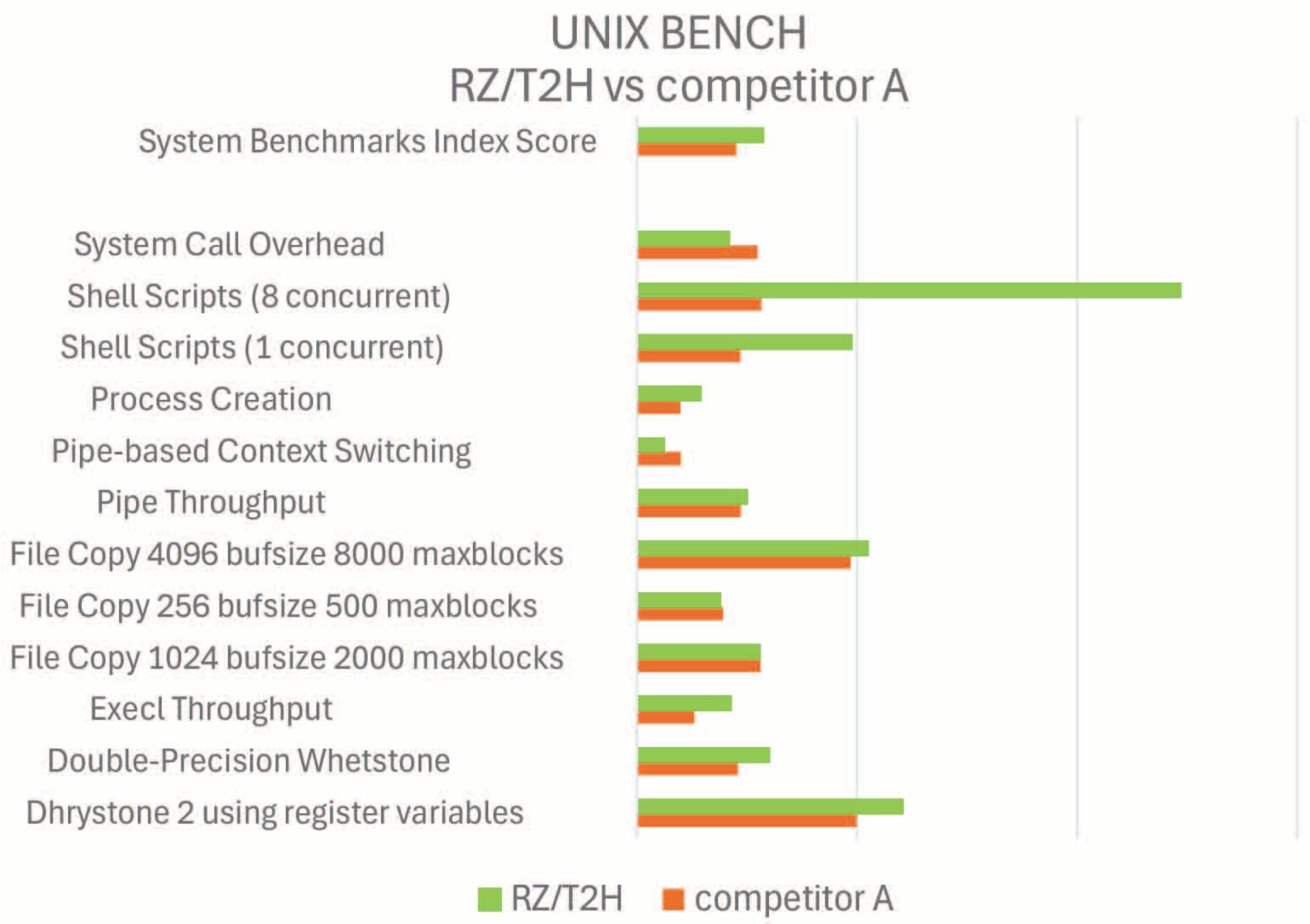
The following graph shows the results of running UNIXBENCH on Linux using an RZ/T2H and a microprocessor from another company which has four application CPUs. The results showed that the RZ/T2H achieves high scores of 35-75% in each category.

The RZ/T2H is equipped with a quad-core Cortex-A55 1.2GHz processor for application processing. It has 32 KB/32 K B L1 I/Dcache per core, and 1024 KB L3 cache implemented as a common cache.
It is possible to speed up the update cycle of the command values for each axis motor and process more complex trajectory planning algorithms by using the RZ/T2H, realizing more precise robot motion.
Multiple Ethernet Communications with Multiple Protocols
In factories using industrial robots, devices from various manufacturers will be connected to a network, and industrial Ethernet protocols such as EtherCAT, PROFINET, and EtherNet/IP, which specialize in real-time communication are used to further increase the synchronization accuracy between devices. The synchronization accuracy between devices has a significant impact on production efficiency, as this is used for simultaneous operations by multiple robots as well as to reduce waiting times.
In conventional industrial robots, dedicated ASSPs have been used to support these multiple industrial Ethernet protocols. In addition to industrial Ethernet, there is a need to have Ethernet communication that is independent of industrial Ethernet
to communicate with PCs and management systems for condition monitoring and software version upgrades, as well as to connect to external HMI devices.
The RZ/T2H is equipped with four external Ethernet ports, three Gigabit Ethernet MACs (GMACs), a Gigabit Ethernet switch (ETHSW), and an EtherCAT® slave controller (ESC); and is compatible with major industrial Ethernet communication protocols such as EtherCAT, PROFINET RT/IRT, EtherNet/IP™, and OPC UA, as well as the next-generation TSN (Time-Sensitive Networking) standard.
Multiple Ethernet implementations are possible by assigning GMAC, ETHSW and ESC to the four external Ethernet ports. For example, two ports can be used for industrial Ethernet, and the remaining two ports can be used for general-purpose Ethernet.

If industrial Ethernet is not needed, up to three ports can be used for general-purpose Ethernet, allowing users to flexibly implement network functions. In addition, the network synchronization signals for ETHSW, such as TDMA and the DC (Distribute Clock) of ESC, are connected to the Event Link Controller (ELC) in the RZ/T2H, making it possible to operate peripheral functions with low latency, and synchronize operations with different devices connected to the network. This enables high-precision synchronization along with linked operation with devices on the network, improving productivity.
This article introduces methods to improve the performance of industrial robots using the RZ/T2H and to significantly reduce the number of components and development time. This enables RZ/T2H users to not only enhance the competitiveness of their industrial robots, but also improve their time to market.
Renesas provides a solution where developers can experience 9-axis motor control using the RZ/T2H. The sample programs for 9-axis motor control can be downloaded from the Renesas website. The RZ/T2H evaluation board and inverter board, which can drive 9-axis motors, are available for purchase from the Renesas online store. For more information, please refer to the RZ/T2H product page.
RZ/T2H: Advanced High-End MPU with Integrated Powerful Application Processing and High-Precision Real-Time Control for 9-Axis Motor Control
RZ/T2H Evaluation Kit: An evaluation and development kit for RZ/T2H
ROS: Robot Operating System is opensource software used in robot development
ORiN: ORiN Consortium - Middleware that connects equipment and integrates systems, overcoming the barriers of standards
■ Renesas Electronics www.renesas.com

In collaboration with Infineon Technologies AG, startup Geomorphing Detection (GMD®) has developed a system that uses radar sensors to continuously monitor streams and rock movements in the Alps. The innovation has the potential to reduce the impact of extreme weather and climaterelated events and protect people and infrastructure.
Natural hazards such as floods, landslides and high tides are on the rise worldwide. In Europe alone, weather- and climate-related events have caused more than 160 billion euros in damage over the past three years, according to a study by the European Environment Agency (EEA). The earlier natural hazards can be detected, the sooner damage to people and infra-
In cooperation with Infineon, the Austrian startup company GMD from Innsbruck/Tyrol has developed an efficient, digital early warning system for monitoring Alpine rivers and areas. The development is based on intelligent PSoC™ 6 microcontrollers and Infineon’s Deepcraft™ Artificial Intelligence (AI)
The system continuously measures important parameters such as water level or flow velocity and detects deformations or dangerous impacts in protective structures such as rockfall nets or avalanche barriers.
“Semiconductor solutions from Infineon are the digital heart of the Internet of

President Connected Secure Systems at Infineon “Our high-performance microcontrollers not only impress with their firstclass features, but also with their wide range of possible applications. We are especially pleased when our solutions can help to save lives, as in this specific case. The easy integration of our microcontrollers into existing systems, their low energy consumption and their high level of safety make it easier for start-ups and developers to implement forward-looking ideas like this.”
Detecting and eliminating obstacles with foresight
In the system, radar technology from Infineon reliably captures data – even in poor lighting and weather conditions –and provides information about the distance, speed and direction of movement of objects. The intelligent AI-based Infineon microcontrollers then process the large amounts of data quickly and precisely. This creates a powerful and efficient system that detects dangers, threats or risks at an early stage in order to remove obstacles and prevent flooding. Thanks to integrated photovoltaics, the intelligent sensor network is also completely energy self-sufficient.
Steve Weingarth, founder and CEO of GMD: “We are delighted to be working with Infineon, a leading international semiconductor company. In combination with our analytics platform, we can offer energy-efficient and cost-effective early warning systems. Since the beginning of our partnership as part of the Infineon Startup Challenge 2024, we have received great support and can already use the system in pilot projects.”

The Alpine region is increasingly affected by natural hazards
In Austria, the system is already being implemented with the city of Kufstein, the state of Tyrol and other municipalities. The aim is to use monitoring to detect blockages in watercourses at an early stage. GMD is also testing the system to record visitor flows at the Prager Alpenhütte in the Hohe Tauern National Park in cooperation with the German Alpine Association (DAV). From July onwards the system will be used to count people on high alpine hiking trails. The more precise recording of visitor flows is intended to improve the water management of the huts and adapt the infrastructure specifically to usage.
Infineon Startup Co-Innovation Program
The global Infineon Startup Co-Innovation Program is a real springboard for many startups. Infineon takes on the role of coinnovator and technology partner and provides the latest components in the fields of energy efficiency, mobility, security, IoT and big data.

Lamin Ben-Hamdane, Head of Startup Cooperations at Infineon: “The cooperation gives the startups access to the latest technologies and our global network. In turn, we benefit from the agile entrepreneurial spirit, learn about innovative system approaches and can better adapt our products to new applications.”
Participation Infineon Startup Challenge 2025
The Infineon Austria Startup Challenge 2025 on the topic “Building Intelligent IoT sensory systems with the help of Edge AI” is currently open. The best startups will then be able to present their prototypes at the Infineon Demo Day in Vienna at the beginning of October. The Startup Challenge is supported by IPCEI ME/CT . Applications are still possible until June 15th.
Further links:
Copyright: Infineon
Infineon Startup Co-Innovation Program: www.infineon.com/startup Application Startup Challenge 2025: https://www.imagimob.com/startupchallenge-2025
About GMD
GMD® GmbH develops intelligent technologies for natural hazard prevention, protecting infrastructure, communities and businesses from the effects of rockfall, landslides, flooding and other natural hazards. Using the GMD GeoSenseAI machine learning platform, IoT sensor technology and real-time data analysis, they enable early detection of risks and an effective response to hazards. Their goal is to increase the safety and resilience of vulnerable regions and support the biodiversity of communities with innovative, sustainable and accurate solutions. Further information: www.gmd.care/en
■ Infineon Technologies www.infineon.com

Wi-Fi, Bluetooth, and Zigbee/Thread combo SoCs support high peak speed and low latency for gaming, AR/VR, entertainment, security, and automotive applications
Synaptics® Incorporated announced it has extended its Veros wireless portfolio with its first family of Wi-Fi® 7 systemson-chips (SoCs) tailored for the Internet of Things (IoT). Comprising the SYN4390 and SYN4384, the scalable offering supports bandwidths up to 320 MHz to deliver 5.8 Gbps peak speed and low latency. The triple-combo SoCs integrate Wi-Fi 7 with Bluetooth® 6.0 and Zigbee/Thread, support Matter, and are designed to minimize system cost and power consumption. They target IoT applications requiring reliable performance-over-range for enhanced user experiences across use cases that include 8K video streaming, interactive gaming, security monitoring, immersive AR/VR, and home and automotive entertainment.
Wi-Fi 7’s multi-link operation (MLO) allows the devices to send and receive a data stream using multiple frequency bands (2.4 GHz, 5 GHz, 6 GHz) simultaneously in support of low latency, reliable connections, and high throughput for real-time applications like video calls and gaming. Synaptics’ architecture provides a power-efficient, cost-effective way to deliver the benefits of MLO.
“Growing adoption of Wi-Fi 7 in wireless networking infrastructure has created an opportunity to address a massive and diverse array of Wi-Fi 7-enabled IoT enduser devices by extending our Veros portfolio,” said Venkat Kodavati, SVP and GM of Wireless Products at Synaptics. “We are bringing the benefits of Wi-Fi 7 in a versatile solution for high-performance, low-power IoT devices. Combined with the ease of integration with our Astra AI-Native compute platform, we expect that developers will have an efficient solution for implementing next-generation connected and AI-enriched IoT products with features such as Wi-Fi Sensing.”
ABI Research forecasts annual shipments of Wi-Fi 7 chipsets to reach more than 2 billion by 2029, achieving a CAGR of 56% between 2024 and 2029.[1]
“Wi-Fi 7 is ushering in a new era of more enriching and sophisticated use cases for connected devices thanks to its channel bandwidth, throughput, and latency improvements,” said Andrew Zignani, Senior Research Director, ABI Research. “However, the requirements for implementation vary
by product type, and edge IoT introduces challenges that differ from PCs or infrastructure applications. Synaptics’ diverse Wi-Fi 7 solutions are tailored to address these unique needs, including low power, support for multiple connectivity protocols, and AI. These will be critical in enabling Wi-Fi 7’s expansion across multiple IoT segments, reaching billions of annual device shipments over the next few years.”
Veros Wi-Fi 7 family highlights
The Veros Wi-Fi 7 IoT family’s support of Matter and its triple combo design provides the interoperability required to allow the devices to serve as versatile home hubs that can operate across Wi-Fi, Bluetooth, and Zigbee/Thread networks in heterogeneous wireless environments. Features support[2]:
• Peak speed of up to 5.8 Gbps, using 2×2 + 2×2 MLO, 320 MHz channel bandwidth, and 4K QAM
• Integrated RF front-end and power management IC (PMIC) that contribute to reduced system cost and power consumption
• Dual-core Bluetooth 6.0 for LE Audio, Channel Sounding, and LE Long Range
• Matter and an integrated 802.15.4 radio capable of enabling Zigbee and Thread networking[3]
• Integrated Arm cores and memory to enable offloading of networking functions from the host processor to help reduce system power consumption[4]
The SYN4390 is available now for sale, and the SYN4384 is available now in limited quantities for evaluation.
[1] Source: ABI Research Article: Wireless Connectivity Technology Segmentation and Addressable Markets by Andrew Zignani (published January 27, 2025) ©2025 Allied Business Intelligence, Inc.
[2] Actual performance may vary based on deployment environment and device configuration
[3] Certification status may vary by implementation
[4] Power savings may vary based on system design and workload
Synaptics www.synaptics.com


This article provides an overview of wireless standards and assesses the suitability of Bluetooth® Low Energy (BLE), SmartMesh (6LoWPAN over IEEE 802.15.4e), and Thread/Zigbee (6LoWPAN over IEEE 802.15.4) for use in industrial harsh RF environments. Comparative metrics are provided, including power consumption, reliability, security, and total cost of ownership. SmartMesh time synchronization results in low power, and SmartMesh and BLE channel hopping result in higher reliability. A case study for SmartMesh concludes with 99.999996% reliability. Analog Devices’ BLE and SmartMesh wireless condition monitoring sensors are presented, including a new wireless sensor with edge artificial intelligence (AI), which increases battery life for constrained edge sensor nodes.

Author: Richard Anslow, Senior Manager Analog Devices
The market for smart sensors for motor driven systems is expected to more than double in sales volume between 2022 and 2024 (growing to $906M USD).1 Within smart sensors, wireless and portable devices are expected to be the primary growth drivers. Monitoring industrial machines using wireless environmental sensors (temperature, vibration) has one clear goal: to detect when the equipment being monitored deviates from healthy operation.
For industrial wireless sensor applications, low power consumption, reliability, and security are consistently ranked as the most important requirements.
Other requirements include low total cost of ownership (minimal gateways, maintenance), short range communication, and a protocol capable of mesh formation for factory environments that include lots of metallic obstacles (meshing networks help to mitigate possible signal path shielding and reflections).
Industrial Applications and Wireless Standards Requirements
Figure 1 provides an overview of wireless standards, and Table 1 ranks selected wireless standards against key industrial requirements. It’s clear that BLE and

SmartMesh (6LoWPAN over IEEE 802.15.4e) offer the best combination of low power consumption, reliability, and security for industrial applications. Table 2 provides more details for the Zigbee/Thread, SmartMesh, and BLE mesh standards.


Table 2: Key Wireless
Table 3: ADI Wireless Industrial Sensor Prototypes
SmartMesh includes a time synchronized channel hopping (TSCH) protocol, where all nodes in a network are synchronized and communication is orchestrated by a schedule. Time synchronization results in low power and channel hopping results in high reliability. The BLE standard also includes channel hopping, but has some constraints in comparison to SmartMesh, including line powered routing nodes (increased system cost and power), and TSCH is not supported.
As previously mentioned, Zigbee/Thread score low on reliability and do not offer many advantages compared to BLE.
This article will focus on SmartMesh and BLE mesh as the most suitable wireless standards for industrial condition monitoring sensors.
Table 3 provides an overview of Analog Devices’ Voyager 3 Wireless Vibration Monitoring Platform and next-generation wireless condition monitoring sensors. Voyager 3 uses a SmartMesh module (LTP5901-IPC). An AI enabled vibration sensor (still in development) uses a BLE microcontroller (MAX32666). Both sensors include temperature and battery state of health (SOH) sensors.
The Voyager 3 and AI version sensors use ADI MEMS accelerometers (ADXL356, ADXL359) to measure vibration amplitude and frequency for industrial equipment. Increasing vibration amplitudes and frequencies are identified using FFT spectra, which can indicate faults such as motor imbalance, misalignment, and damaged bearings. Figure 2 provides an overview of a typical operation for Voyager 3 and the AI enabled vibration sensors.

Like many industrial sensors, the duty cycle is 1%; most of the time the sensor is in a low power mode. The sensor wakes up periodically for bulk data gathering (or in a high vibration amplitude shock event) or to send the user a status update. The user is typically notified with a flag to state that the monitored machine is in good health, and the user is given the opportunity to gather more data.
SmartMesh IP networks have several layers of security, which can be categorized as confidentiality, integrity, and authenticity. A summary of SmartMesh security is provided in Figure 3. Confidentiality is achieved with AES-128-bit encryption end to end, even if there are multiple mesh nodes in the network. Data transmitted is protected by message authentication codes (message integrity check, or MIC) to ensure that it has not been tampered with. This protects against man in the middle (MITM) attacks, as shown in Figure 3. Multiple device authentication levels are possible, which prevents unauthorized sensors from being added to the system. Devices operating with versions 4.0 and 4.1 of the BLE standard are security vulnerable, however, versions 4.2 and above include enhanced security (as described in Figure 3). ADI’s MAX32666 is compliant to the BLE standard 5.0. This version introduces the P-256 Elliptic Curve DiffieHellman key exchange for pairing. In this protocol, the public keys of the two devices are used to establish a shared secret between the two devices, called the long-term key (LTK). This shared secret is used for authentication and generation of keys to encrypt all communication, protecting against MITM attacks.
The sensors described in Table 3 operate on a 1% duty cycle, with Voyager 3 maximum payload of 90 bytes, and the AI version maximum payload of 510 bytes. Figure 4 (adapted from Shahzad and Oelmann3) shows that for 500 bytes to 1000 bytes, BLE consumes less energy compared to Zigbee and Wi-Fi. BLE is thus a good match for the AI enabled use case. SmartMesh provides ultra low power consumption, especially for payloads of 90 bytes or less (as used in the Voyager 3 sensor). The SmartMesh energy consumption is estimated using the SmartMesh Power and Performance Estimator tool available on the website.
The SmartMesh power estimator tool accuracy has been experimentally verified 87% to 99% accurate depending on whether a sensor is a routing or leaf node. In addition to radio transmit power consumption, one must consider the total system power budget and total cost of ownership.
As described in Table 2, BLE and Zigbee both operate using a single gateway. However, both also require line power for routing nodes. This increases the power budget and total cost of system owner-
ship. In contrast, SmartMesh routing nodes only require on average 50 μA of current, and an entire network can operate using a single gateway. SmartMesh is clearly a more energy efficient implementation.
As mentioned previously, SmartMesh uses TSCH, which has the following characteristics:
• All nodes in a network are synchronized.
• Communication is orchestrated by a communication schedule.

3
Security implementation for BLE and SmartMesh networks.
Robust communications Nodes interfere with each Efficient channel allocation Relies on collisions that in densely formatted other, slowing down eliminates collisions slow down network networks network
Long battery life when Requires power efficient edge
Battery-powered routing Line-powered routing nodes sensors mounted in node connections to meet nodes establish close range establish close range shielded locations battery lifetime specs connection to edge nodes connections to edge nodes
Reliable connections in RMovement of equipment Employs channel hopping Employs channel hopping to dynamic industrial or opening/closing of doors to avoid reception nulls avoid reception nulls environments cause multipath reflections
Reliable communications Interferers restrict data traffic Channel hopping to avoid Designed for small networks in congested radio bands bandwidth on the network interferers and efficient and suffers from network bandwidth allocation flooding maintains traffic
Table 4: Key Challenges for Wireless Networks in Industrial Application and BLE/SmartMesh Performance
• Time synchronization results in low power.
• Channel hopping results in high reliability.
• The scheduled nature of communication brings a high level of determinism.
The synchronization accuracy is less than 15 μs across the entire network. This extremely high level of synchronization results in extremely low power. On average 50 μA current draw, and 1.4 μA greater than 99% of the time.
Wireless industrial sensors currently available on the market typically operate on very low duty cycles. The user sets the sensor sleep duration, after which the sensor wakes up and measures temperature and vibration, and then sends the data over the radio back to the user’s data aggregator.
Commercially available sensors typically quote a 5-year battery life, based on one data capture every 24 hours, or one data capture every 4 hours.

Table 4 provides some key application challenges and how SmartMesh and BLE mesh meet these challenges.
SmartMesh performs better for dense networks with large numbers of nodes. Both BLE and SmartMesh perform well in dynamic industrial environments. The reliability of SmartMesh was tested in ADI’s wafer fab facility.5 This is a harsh RF environment, with dense metal and concrete. Thirty-two wireless sensor nodes were distributed in a mesh network, with four hops between the furthest sensor node to the gateway. Four data packets were sent every 30 seconds from each sensor node. Over a time period of 83 days 26,137,382 packets were sent from the sensors, with 26,137,381 packets received, resulting in 99.999996% reliability.
The next-generation sensor will operate in a similar fashion but take advantage of Edge AI anomaly detection to limit the use of the radio. When the sensor wakes up and measures data, the data is only sent back to the user if a vibration anomaly is detected. In this way the battery life can be increased by at least 20%.
BLE can operate more reliably and at lower power compared to Zigbee and Thread for networks requiring 500 bytes to 1000 bytes of data transmission. Microcontrollers with embedded AI hardware accelerators provide a path to better decision-making and longer battery life for wireless sensor nodes.

Richard Anslow is a senior manager, working in the field of software systems design engineering within the Industrial Automation Business Unit at Analog Devices. His areas of expertise are condition-based monitoring, motor control, and industrial communication design. He received his B.Eng. and M.Eng. degrees from the University of Limerick, Limerick, Ireland. Recently, he completed a postgraduate program in AI and ML with Purdue University.
References
1) “Predictive Maintenance in Motor Driven Systems – 2020.” Interact Analysis Market Study, April 2020.
2) Kris Pister and Jonathan Simon. “Secure Wireless Sensor Networks Against Attacks.” Electronic Design, April 2014.
■ Analog Devices www.analog.com Data transmitted (radio transceiver PHY) and energy consumption. (adapted from Shahzad and Oelmann)3 © ADI
The next-generation wireless sensor includes the MAX78000 microcontroller with AI hardware accelerator. This AI hardware accelerator minimizes data movement and leverages parallelism for optimal energy use and throughput.
For AI model training the sensor collects healthy data for the machine, which is then sent over the air to the user for AI model development. Using the MAX78000 tools the AI model is synthesized into C code, and then sent back to the wireless sensor and placed in memory. When the code is deployed the wireless sensor wakes up at predefined intervals, or in a high-g shock event. Data is gathered and an FFT is generated. From the FFT, the MAX78000 makes an inference based on this data. If no anomaly is detected the sensor goes back to sleep. If an anomaly is detected the user is notified. The user can then request FFT or raw time domain data for the measured anomaly, which can be used for fault classification.
This article provides an overview of wireless standards and assesses the suitability of BLE, SmartMesh (6LoWPAN over IEEE 802.15.4e), and Thread/Zigbee (IEEE 802.15.4) for use in industrial harsh RF environments. SmartMesh has superior reliability and low power operation compared to BLE and Thread/Zigbee.
3) Khurram Shahzad and Bengt Oelmann. “A Comparative Study of In-sensor Processing vs. Raw Data Transmission Using ZigBee, BLE and Wi-Fi for Data Intensive Monitoring Applications.” 11th International Symposium on Wireless Communications Systems (ISWCS), August 2014.
4) Thomas Watteyne, Joy Weiss, Lance Doherty, and Jonathan Simon. “Industrial IEEE802.15.4e Networks: Performance and Trade-offs.” 2015 IEEE International Conference on Communications (ICC), June 2015.
5) Ross Yu. “Verifying SmartMesh IP >99.999% Data Reliability for Industrial Internet of Things Applications.” Analog Devices, Inc. January 2016.

Engage with like-minded members and ADI technology experts in our online community, EngineerZone®. Expand your network, ask your tough design questions, share your expertise, browse our rich knowledge base, or read about new technologies and the engineers behind them in one of our blogs. Visit https://ez.analog.com


Author: Tim Morin, Technical Fellow – FPGA business
Microchip Technology
Is cybersecurity all you need? Even though your system may be protected by “physical” security including fences, gates, guards and cameras, is that enough?
For companies building next-generation weapons systems for the military, the answer is clear.
But what about the broader nondefense market? What about designs destined for industrial, energy, communications or automotive applications?
Cybersecurity is not enough. If you start thinking about security when designing your software, you’re already too late. All of the equipment you create will fall into the hands of your competitors and bad actors. So, your hardware must be secure from the ground up.
So ... under what conditions could a bad actor have access to a piece of your equipment? And what could they do to exploit your equipment’s function, extract its data, or even steal your intellectual property? Does equipment ever get “lost?” How does equipment get decommissioned? Who services your equipment and how is it upgraded?
The answers lie in whether your supply chain is managed securely.
There are three critical areas to consider –the areas where electronic systems are the most vulnerable.

And, thankfully, there are things you can put in place to address that.
• Manufacturing - building your printedcircuit board, assembly and test. During programming of non-volatile devices, are you using hashed and signed images? Is there an auditable log of what’s been provisioned, the number of boards that have been provisioned and the number of boards that have failed outgoing test? Are these logs hashed and signed? Also, are debug ports disabled?
• Shipping to your clients, distributors and resellers. Can you account for units shipped versus units received by your customer? Most customers will tell you right away, “hey were short one!” But what if the customer missed one, for any reason? You would have to assume you have a piece of equipment in the wild. Also, can you and your customer verify the integrity of the equipment shipped? And that it hasn’t been tampered with in transit?
• Managing deployed equipment. Are there anti-tamper seals on the equipment? Are only authorized technicians allowed to service equipment? Are remote updates allowed? And if so, are the images verified to be intact and authentic? Are there mechanisms in place to prevent roll backs? And finally, when equipment is de-commissioned is it zeroized? Made inoperable? Destroyed?
If the answer is “no” to any of the above, you should strongly consider semiconductors that have anti-tamper countermeasures built-in so you can tailor your tamper responses to the risk scenarios a piece of equipment is likely to see during its life cycle. Here are some of the most important features to look for:
– Digital tamper flags
– Ensure your selected hardware device has analog windowed voltage detectors that give you high and low trip points for each critical supply. It is important for these detectors be high speed analog comparators to detect voltage glitches which are sometimes used to trigger faults in the device.
– Digital windowed temperature – this gives you a high and low die temperature – Raw voltage and temperature values from a built-in temperature detector
– A system controller slow clock indicating a system controller brownout condition
– A digital bus that indicates the source of a device reset – whether it’s a DEVRST pin, tamper macro input, system controller watchdog, security lock tamper detectors have fired, or any other type of reset.
For more information on physically securing your designs, check out this security user guide, or drop in on this Security University class. More information on the anti-tamper and other physical security features of the PolarFire® family of products –which can be customized in response to a specific threat profile – is available here
■ Microchip Technology www.microchip.com


Author: Dustin Tenney, Senior Product Marketing Engineer Microchip Technology
The clean and efficient design of hybrid and electric vehicles, from an increasingly growing number of suppliers, draws the attention of many as they drive the movement toward sustainable solutions through the electrification of motor vehicles. With the introduction of a variety of electric motors and batteries, an old problem manifests itself at a high level in the electronics world: stray magnetic fields. This electro-magnetic interference (EMI) wreaks havoc on current popular position sensor solutions that do not have an inherent immunity such as hall effect sensors, or that can have immunity but are costly to implement like magnetic resolvers and linear variable differential transformers (LVDT).
Ergo the introduction of the inductive position sensor which provides high accuracy position sensing despite being immersed in a stray magnetic field rich environment.
Magnetic fields are not an unknown artifact or even a newly discovered element in the semiconductor and electronics world. They are part of the integral function of semiconductors and are considered in the design of every chip. However, when brushless direct current (BLDC) motors, permanent magnet synchronous motors (PMSM), motor currents or large battery currents are in proximity to electronics modules and sensors, the stray magnetic fields cause interference and may even induce failures in safety critical applications.
BLDC and PMSM motors are some of the most common drive motors used in electric and hybrid two-and four-wheel vehicles Both motors use very strong magnets on the rotor and function when currents flow from the motor controller and are applied to the stator to activate the electromagnets. Both the magnets and the currents used in the motor emit EMI into the areas around them. Other BLDC motors are present in many areas of a vehicle including brake and steering motors. Also critical to the design of all electric vehicles and a contributor to the presence of stray magnetic fields are batteries, more specifically, the source of the EMI being the electrical current that flows when high currents are charging the batteries or powering the vehicle.
Some vehicles use several thousand batteries to send current to the system which makes them a major contributor to the stray magnetic fields that cause problems in traditional sensor solutions.
Position sensing is a critical part of the design of many electronics, including those found in a variety of applications within vehicles such as foot pedals, throttle control, brake positioning, transmission tracking, infotainment knobs, gear shifts, steering sensors and more. Historically magnetic resolvers, linear variable differential transformers (LVDT) and hall effect sensors have been used as the main method of position sensing. Hall effect sensors are one of the most widely implemented solutions and are designed to determine the strength and the direction of a magnetic field, thus being able to determine the position of a magnet or electromagnet placed near to the sensor.
The sensing portion of this device is a thin piece of silicon, which when exposed to a magnetic field will push electrons and holes to opposing edges of the silicon. This creates a very small voltage potential known as the Hall Effect and requires strong magnetic fields to produce a sensing environment. When EMI is added into the equation, Hall Effect sensors face the danger of distorted, premature or false magnet detection and can risk permanent damage. To reduce the risk of failure caused by EMI, the use of magnetic absorbing metals is implemented to shield the sensor from stray magnetic fields, which increases the size and cost of the solutions.
An increasingly popular solution to reduce risk, cost and size in EMI laden applications is the inductive position sensor. These sensors are not magnetic, nor do they need to use magnets or magnetic metals, but are as the name suggests, an inductor-based solution.
Through the design of the sensor body, which is a thin PCB with an embedded winding of metal traces, passive rejection of EMI is achieved. As a conductive piece of metal, called a target, is passed over the sensor the magnetic fields emitted by the primary coil on the PCB (similar to the primary on a transformer) are disrupted and the magnetic field drops to zero where the target is located.
Also embedded in the PCB are two receive coils (secondary of the transformer) that are used to detect the different voltages caused by the disturbance of the magnetic field. The resultant information is processed at the IC to return the position-based output value to the system. Built into the design of these devices are the key methods to reject stray magnetic fields that would normally interfere with the system.
Active and passive noise filtering are some of the key features implemented by design in many inductive position sensors. Active rejection of stray magnetic fields is achieved through the wellknown technical properties of synchronous demodulation and bandwidth filters. Combining these techniques allows specific signals to be measured, while ignoring the otherwise intrusive noise from the environment.
The transmitter and receiver originate in the same system and so we are able to calculate the exact phase between the two signals and actively reject magnetic field noise. Passive filtering is enabled by the use of the voltage detection coils. The disturbance detected on these coils can be used to calculate the exact position based on a ratio of sine and cosine.
Metals outside the effective air gap range are not registered in the sensing circuit due to the use of the ratio metric calculations using the signals from the receive coils. The implementation of these noise rejection methods provide highly accurate position detection that is immune to stray magnetic fields while removing the need for heavy and expensive magnets, or EMI shielding.
In support of these claims of incredible EMI immunity the team at Microchip Technology has collected evidence through experiments on the inductive position sensors with induced magnetic fields in close proximity to the sensor. In one experiment a neodymium magnet was placed approximately 15 mm above the linear PCB sensor body using an acrylic structure in such a way that the target would pass freely under the magnet, and the magnet could also be moved statically or dynamically along the sensor body. A gaussmeter probe was also placed along the sensor to detect the strength of the magnet.
Although the probe detected a 7.2 mT (5716.9 A/m) magnetic field there was no influence on the precise sensing of the position of the target as it was moved along the PC. Other tests according to ISO11452-8 automotive standards prove the immunity levels of these encoders meeting level IV and even surpassing those levels to achieve a 7,000 A/m (8.8 mT) electromagnetic conductance immunity at a 10 Hz.
The inductive encoder technology consistently performs without interference despite magnetic fields being forced into the sensor. The accuracy and precision of the target detection is not diluted or distorted due to the synchronous demodulation and the operating frequency of the IC design.
As modern design requirements demand a continually shrinking form factor while maintaining or improving performance, the inductive position sensor lends itself as a fantastic upgrade to aging magnetic solutions. The same IC can support linear and rotary position sensing designs using a simple PCB sensor body and a small metal target.
This solution is immune to stray magnetic fields while maintaining very high accuracy and is capable of supporting high reliability (AEC Q100 Grade 0) and safety rating support (ASIL D). Pushing ahead in this movement to inductive position sensing, Microchip’s portfolio is the most comprehensive in the industry supporting a plethora of low and highspeed sensing applications including motor control.
These sensors are a perfect fit for precision position sensor designs, including those where high levels of magnetic interference is present.
Design resources:
Microchip Inductive Position Sensors.
■ Microchip Technology www.microchip.com


Author: Kerstin Naser, Corporate Product Manager Wireless Rutronik

Following the release of the Wi-Fi 6 and Wi-Fi 6E standards, the Wi-Fi Alliance introduced the latest IEEE 802.11be standard, also known as Wi-Fi 7, earlier this year. WiFi 7 offers even higher data transmission rates and extremely low latency times. This standard thus meets the requirements for applications like augmented, virtual, and extended reality.
While many users continue to use Wi-Fi 5, Wi-Fi 6 or Wi-Fi 6E have now also gained a strong foothold in the market. Some sup-
Wi-Fi 7 utilizes more efficient frequency bands, multilink operation, and 320 MHz channel width to deliver higher speeds of up to 46 Gbps, reduced latency, and enhanced network reliability. Applications with real-time requirements in particular benefit from the performance improvements.
pliers already offer Wi-Fi 7-compatible products. The Wi-Fi Alliance projects that by 2028, there will be 2.1 billion Wi-Fi 7enabled devices available on the market. Routers, smartphones, PCs, and tablets are among the first devices to support the new standard [1], but Rutronik also already provides solutions for the industrial sector, as detailed in our Wi-Fi 7 catalogue. Table 1 shows the development and differences of the Wi-Fi standards from Wi-Fi 5 to the latest standard Wi-Fi 7.
The Wi-Fi Alliance identifies key applications for Wi-Fi Certified 7 as multi-user AR/VR/XR, 3D training, gaming, ultra-highresolution video streaming, hybrid working, Industrial IoT (IIoT), and automotive[1] However, thanks to the high reliability and speed of data transmission, ultra-precise applications like tele diagnostics and telesurgery are also feasible. The necessary increase in performance results from the following seven features[1]:
1. 320 MHz channels: Available in countries that release the 6 GHz frequency band for Wi-Fi. Ultra-wideband channels double the currently widest channel size of 160 MHz for Wi-Fi 6/6E to 320 MHz, also effectively doubling the data transmission rates for individual devices.
2. Multilink operation (MLO): With the previous WLAN standards, routers select a single frequency band for data transmission and switch frequency bands only under specific conditions. With Wi-Fi 7, MLO allows devices to simultaneously send and receive data across multiple frequency bands, such as 5 GHz and 6 GHz. This results in higher data throughput, lower delay times, and improved reliability.
3. 4K QAM: Wi-Fi 7 enables a higher data transmission rate. This data transmission rate is specified by the modulation technique called quadrature amplitude modulation (QAM). Compared to 1,024 QAM with Wi-Fi 6/6E and only 256 QAM with Wi-Fi 5, 4,096 QAM (or 4K QAM) are possible with Wi-Fi 7. 4K QAM now enables up to 20 percent higher data rates (12 bits instead of 10 bits).
4. 512 compressed block acknowledgment: With Wi-Fi 7, up to 512 data packets (MPDUs – MAC protocol data units) can be sent simultaneously, compared to 256 data packets with Wi-Fi 6. This reduces overheads, thereby enhancing overall efficiency.
5. Multiple resource units (RU) to a single station (STA): Improves flexibility in planning spectrum resources to increase spectrum efficiency. This is achieved because Wi-Fi 7 divides the channel into multiple sub-channels, known as resource units (RUs). This procedure is similar to the OFDMA procedure of Wi-Fi 6. By dividing the channels, interference signals affect only a portion of the WLAN channel rather than the entire channel, as was the case with previous Wi-Fi standards. The remaining part can, therefore, still be used for data transmission.
6. Triggered uplink access: Optimizes the uplink access as defined by Wi-Fi 6 to better handle latency-sensitive streams and meet quality of service (QoS) requirements. The stream classification service (SCS) function prioritizes sensitive data such as games, voice, and video over bulk traffic by “classifying” data.
7. Emergency preparedness communication services (EPCS): 7. Emergency preparedness communication services (EPCS): Offer users a seamless NSEP (national security and emergency preparedness) service experience while maintaining priority and quality of service (QoS) on Wi-Fi access networks. EPCS enables access points (APs) to communicate with authorized non-AP stations with higher priority.
Applications with real-time requirements benefit from the significantly improved latency. To achieve the theoretical maximum data transmission rate of 46 Gbps, WLAN stations with 16 data streams (spatial streams), i. e. also 16 antennas, are required. In practice, this is not practical for small devices like cell phones. For typical home use, routers with fewer antennas are generally sufficient.
However, it definitely makes sense for large companies, smart cities, airports, hotels, etc. with numerous end users.
First products available
To fully leverage the performance and efficiency of the new standard, products that support Wi-Fi 7 must meet certain requirements. The devices must be equipped with Wi-Fi 7-compatible chipsets that support the new functions and higher speeds. Moreover, the products must also be able to use several frequency bands at the same time to enhance network performance. In addition, support for 4,096 QAM is required for higher data density and efficiency. Rutronik already offers Wi-Fi 7capable routers, mainboards, expansion cards, industrial modules, and laptops.
Intel’s BE200 and BE202 modules fully support the benefits of the new wireless standard, above all low latency times, high reliability, and high speeds: BE202 enables 2.4 Gbps with 2 x 2 TX/RX streams, BE200 even 5.8 Gbps. Both solutions also support the Bluetooth 5.4 standard. Additionally, these modules are pre-certified globally, resulting in significant cost savings for customers. However, VPRO support is currently only possible for BE200. Versions for the industrial temperature range or embedded applications are also not yet available. Both cards can be obtained in the M.2 2230 and M.2 1216 form factors.
Silex has also announced a Wi-Fi 7 platform with SX-PCEBE. Like Intel’s products, the SX-PCEBE plug-in card will also be on

offer in two form factors, as an M.2 2230 plug-in board and as an SMD M.2 LGA type 1620. In addition to Wi-Fi 7, the module also supports Bluetooth 5.3, is based on the Qualcomm QCC2076 chipset and features an operating temperature range of –40 °C to +85 °C. The first samples of this module are expected by the end of 2024, with series production planned for the first quarter of 2025.

Besides the plug-in card solutions mentioned, Rutronik already offers complete Wi-Fi 7 routers and mainboards from Asus, as well as special avionics routers from Advantech. Wi-Fi 7 chips from Mediatek are now available for expert developers and high-volume projects. Suitable Wi-Fi 7 antennas from 2J and Kyocera AVX can also be obtained from Rutronik.
Summary
Like Wi-Fi 6E, Wi-Fi 7 supports the 6 GHz frequency band – an advantage, as the 2.4 GHz frequency band is also used by other technologies such as Bluetooth, ZigBee, and Thread. However, keep in mind that higher frequencies also result in shorter ranges. To ensure comprehensive WLAN availability, it may therefore be necessary to increase the number of access points.
Despite the backward compatibility of Wi-Fi 7 with previous standards, not only the routers but also the end devices must support Wi-Fi 7 to fully leverage the benefits of Wi-Fi 7.
Referință:
[1] Wi-Fi Alliance® introduces Wi-Fi CERTIFIED 7™ | Wi-Fi Alliance
■ Rutronik www.rutronik.com


Shawn Luke, Technical Marketing Engineer

Michael Williams, Director of Marketing Industrial & Infrastructure

Experts from two industry-leading semiconductor companies –Michael Williams, director of marketing for industrial and infrastructure at Infineon Technologies and Shawn Luke, technical marketing engineer at DigiKey – share their thoughts on how SiC technology has impacted the market and what’s next.
Silicon carbide (SiC) has become a cornerstone for enhancing efficiency and supporting decarbonization across industries. It’s an enabler for advanced power systems, addressing growing global demands in renewable energy, electric vehicles (EVs), data centers and grid infrastructure.
SiC technology has advantages over traditional silicon devices, especially in power conversion efficiency and thermally sensitive situations.
Its overall impact in the electronics and power industries can lead to greater profitability and sustainability.
Shifting power consumption
“In the past, most power consumption was tied to some type of motor control such as industrial automation applications and factories, rail transportation, moving pumps for wastewater treatment or fluids like oil in pipelines,” said Williams
“With the introduction of silicon carbide,
there was a shift toward driving efficiency in the marketplace, enabling reductions in energy losses across multiple conversion stages, supporting high-demand applications.”
This shift focused on decarbonization and the development of new generations of renewable technology, including renewable energy systems, EV infrastructure and data centers. It also improved power conversion efficiency from around 95% to 98.5%, a significant shift that has lowered energy losses, reduced heat generation and minimized cooling requirements.
Grid infrastructure
Simply transferring power from the grid or a high-voltage power line into a data center can result in a 5-6% loss in power as it travels through several layers of conversion. Data centers alone are estimated to account for 3% of global energy consumption today, projected to rise to 4% by 2030 (Data Centre Magazine, 2022), with no expectations of slowing down.
SiC comes into play for datacenter power infrastructure, driving efficiency and system cost in grid-scale energy storage and solar central inverters. The combined solution enables future datacenters to work in a microgrid environment, reducing loading on the already strained U.S. grid.
“With the electrification of automobiles, we’re seeing many reference designs come out with bi-directional charging and advanced power electronics, meaning they’re charging during non-peak times and putting power back into the grid for peak times,” said Luke.
SiC, as a wide-bandgap technology, supports higher voltage handling and faster switching speeds in applications like EV charging. This has enabled a complete transformation of the global grid infrastructure while reducing system complexity and overall costs.
Designing with SiC technology SiC technology addresses efficiency well, but there are times when a designer needs a small product, which is when wide bandgap (WBG) or silicon (Si) devices are used.
“Just as a designer has three technologies to choose from, they also have three fundamental design considerations. Do I make my product cost-effective; do I make my product compact; or do I make my product efficient?” explains Williams. “Choosing any two of these priorities allows a designer to choose Si solutions. However, designing for all three of these considerations requires wide bandgap devices. The key driver for compact products is increasing the switching frequency to reduce the size of the magnetics and capacitance in the system.”
Because of the WBG capability in SiC technology, voltage levels can be higher, which has enabled the next generation of technology implementation. The challenge is that SiC is a complex material to work with given it’s a significantly stiffer base material than traditional silicon.
Power cycling is a key factor in package development, as it puts strain on the interconnection between the SiC die and its leadframe or substrate, potentially leading to premature device failure. Developing new interconnection technologies to improve the power cycling performance of future SiC devices is important in addressing the future requirements of a decarbonized grid.
“Applications now utilize much higher power cycling than the motor-drive applications of the past,” said Williams. “Infineon has been focused on developing our .XT technology, an advanced interconnection technology proven to increase power cycling performance >22 times versus standard soft solder techniques. This technology development enables higher power density, improved thermal performance, and maximum system lifetime, enabling the shift to more renewable energy sources.”
Power conversion market innovations
One area these experts are excited about is the decarbonization of the grid, which involves transitioning away from fossil fuel power plants (like coal and oil).
“Decarbonization can happen both at the macro level with changes power companies are making to switch to wind, solar and hydropower, but also at the consumer level through EVs and the like,” said Luke.

“Enablers like SiC are helping us get closer to microgrids more than ever before, localizing power sources for less conversion and loss, aiding in decarbonization.”
Another innovation they see as having a strong impact on the power sector is the implementation of solid-state transformers. These can greatly enhance the infrastructure of the power grid, reducing the size, installation time and overall complexity of the utility site. Deploying solidstate transformers enables modular, high-voltage systems and microgrid solutions, leading to more sustainable power distribution.
What’s next?
With new technology rolling out constantly, SiC is predicted to have a lasting presence.
“Infineon experts predict silicon power switching devices will continue to dominate the market for the remainder of the decade,” said Williams. “We have a unique position in the market by offering all three switching technologies: silicon, silicon carbide and gallium nitride and see no threat from wide bandgap power devices reducing the total market size.”
Companies like Infineon are investing in scaling manufacturing to increase capacity and developing solutions that improve power efficiency while reducing the cost of SiC technology. Innovations such as modular microgrids, distributed DC networks, and fusion reactors are on the horizon, with SiC at the core of these advancements.
Through a strong partnership with its global distributor, DigiKey, the rapid deployment of new technologies through a no-minimum-order and high-availability distribution model, designers and engineers are well-positioned to run with all that is next. For more information on power solutions, visit DigiKey.com.
■ DigiKey www.digikey.com


The growing complexity of the supply chain demands innovative solutions: traceability at the product level in particular is placing increasing demands on manufacturers and distributors. COMI (collective mind) and Rutronik Elektronische Bauelemente GmbH have jointly taken a decisive step towards smarter logistics: the implementation of camera-based AI goods recording has raised the processes in the broadline distributor's largest logistics center to a new, highly economical level, while also making work easier for the employees there.
Authors: Christian Krebs, Head of Project & Process Management, Rutronik Markus Förste, Head of AI, COMI (collective mind GmbH)
Time-consuming and error-prone processes
At the Rutronik logistics center in Eisingen, 48 workstations are dedicated to incoming goods alone. With over 100,000 electronic components available and the associated variable data to be recorded, the manual inspection and documentation of incoming goods posed a major challenge. The existing manual process was timeconsuming and prone to error, which led to discrepancies in the inventory data and a high workload. In addition, important additional information such as article numbers, batch data or countries of origin were not systematically recorded, which significantly affected traceability and quality assurance.
This had an impact on the direct efficiency of the incoming goods process and longterm consequences for downstream logistics and quality assurance.
Since incorrect or incomplete data can lead to delays, higher costs and problems in the traceability of products, a solution was needed that would address these weaknesses in a sustainable way while also meeting the increasing demands on modern logistics systems.
Automation and data integration
Rutronik therefore set itself the goal of automating the incoming goods process with the help of an innovative system to increase efficiency, reduce errors and digitize logistics. The solution should enable reliable item recognition and quantity checking in real time, automatically read label contents such as item numbers and production data, and seamlessly integrate the captured data into existing systems. The employees in the incoming goods department should be relieved of time-consuming manual processes.
At the same time, the system had to be flexible enough to adapt to different requirements, whether it be the integration of new product types or the adaptation to changing operational conditions.
Camera-based, flexible system with artificial intelligence
The solution developed by COMI is based on an industrial-grade camera system that has been combined with state-of-the-art AI algorithms and user-friendly software that can be customized to meet individual customer requirements. The system recognizes label content such as QR codes, barcodes and text segments, regardless of their position or orientation.
Another advantage: several labels – even from several items or packages – can be read in parallel at one workstation, which significantly optimizes the work process in terms of time.

The captured data is then processed using parser algorithms so that information and entities such as article numbers, production data, quantity specifications and countries of origin are available in a structured form. This data is transferred directly into the existing system and can be accessed immediately. Real-time visualization allows users to view the read information directly on a visual front end, which increases transparency and enables immediate verification. The system is also particularly robust and adaptable. Even in difficult or changing light conditions, as well as when dirty, the performance remains constant. The flexibility of the system allows for easy integration into different environments and it can be continuously developed through software updates. By using synthetic data, the AI can also be trained with realistic scenarios in CAD models before commissioning. This saves time and resources, as costly data collection in the production environment is minimized. At the same time, the AI's high accuracy is ensured because it is built on a broad database.
The platform change to an AI-based system solution brings significant improvements in a short time. Human error is almost eliminated and data quality is significantly increased. The time saved is considerable, as the automated process is much faster than the previous manual
inspection; for example, the average inspection time per article has been reduced by over 50%.
The structured storage of all relevant information enables seamless traceability and facilitates downstream analysis. This is particularly beneficial in industries with strict regulatory requirements (e.g. medical/pharma or automotive).
The system also generates detailed reports that document the entire lifecycle of a product, thus increasing transparency in the supply chain. It can easily be extended to other use cases, such as quality control or production monitoring, making it a sustainable investment in the digitalization of logistics processes.
The collaboration between COMI and Rutronik Elektronische Bauelemente GmbH shows how AI technologies can fundamentally transform industrial and supply chain processes. The success of this project highlights the importance of a practical implementation that combines the expertise of both companies in AI and modern hardware.
This innovative approach not only overcomes current challenges, but also creates a solid basis for future innovations by increasing efficiency, minimizing errors, and enabling the growing demands of the market to be met.
For developers and companies, this system offers a practical entry point into smart production and logistics, thus providing real added value in a digitalized world. Not only does it make a significant contribution to optimizing the supply chain, but it also serves as a model for other industries that have to overcome similar challenges. The future of logistics is intelligent, connected, and flexible –and this use case is proof of how this vision is becoming reality.
About the collaboration between Rutronik Elektronische Bauelemente GmbH and collective mind GmbH Since October 2024, Europe's leading broadline distributor Rutronik has held a 30 percent stake in COMI (collective mind), an expert in machine vision applications in the AI environment. The companies are thus combining their strengths in component distribution with automated image processing to offer internationally scalable and developed software and hardware solutions for AI applications in retail and industry, among others, from a single source.
■ Rutronik www.rutronik.com

Renesas Electronics expanded its RZ/V Series of microprocessors (MPUs) with RZ/V2N that targets the high-volume vision AI market. Similar to its high-end device, the RZ/V2H, the new RZ/V2N MPU comes with Renesas’ proprietary AI accelerator, DRP (Dynamically Reconfigurable Processor)-AI3, boasting 10 TOPS/W (Tera Operations Per Second Per Watt) power efficiency and an AI inference performance of up to 15 TOPS through its advanced pruning (Note 1) technology. With the latest addition of the RZ/V2N, the RZ/V series has now expanded to cover a full range of markets, from the low-end RZ/V2L (0.5TOPS) to the highend RZ/V2H (up to 80 TOPS).
The new MPU is significantly smaller than the RZ/V2H, with its package area measuring only 15 mm square, reducing the area required for mounting by 38%.
Inheriting the advanced features of the RZ/V series, the RZ/V2N combines high AI performance with low power consumption. These optimized features suppress heat generation, eliminating the need for additional cooling fans and reducing the size and cost of embedded systems. Developers can easily implement vision AI in a wide range of applications, from AI cameras for traffic and congestion analysis in commercial facilities, industrial cameras for visual inspection on production lines, to driver monitoring systems for behavior analysis.
Similar to the RZ/V2H, the new RZ/V2N MPU is equipped with four best-in-class Arm® Cortex®-A55 CPU cores and a single Cortex -M33 core, coupled with a high-quality image signal processor (ISP), Arm Mali-C55.

The RZ/V2N also has two channels of MIPI camera interfaces, which allow two cameras to be connected to capture doubleangle images. The two-camera system significantly improves spatial recognition performance compared to a single camera system and enables more precise human motion line analysis and fall detection. Furthermore, the dual-camera system captures images from different locations, allowing a single chip to count cars in a parking lot and recognize license plates efficiently.
The RZ/V2N MPU will be available with the Renesas evaluation board kit and a software development environment, along with various AI applications covering more than 50 use cases that are provided in the AI Applications and AI SDK (GitHub). The SDK assists users without in-depth AI knowledge to quickly evaluate and develop AI applications, shortening time to market. Additionally, partner companies will provide a SOM (systemon-module) board, SBC (single board computers), camera modules, and other products that incorporate the Renesas RZ/V2N. This reduces hardware design work, allowing developers to focus on AI application development and bring their products to market rapidly.
Renesas has developed the AI Camera Solution, which targets a variety of applications, including factories, public facilities, and commercial facilities. This solution consists of the RZ/V2N, power management IC, and real-time clock IC, and can be used as a reference for AI camera systems. Winning Combinations are technically vetted system architectures from mutually compatible devices that work together seamlessly to bring an optimized, low-risk design for faster time to market.
Renesas offers more than 400 Winning Combinations with a wide range of products from the Renesas portfolio to enable customers to speed up the design process and bring their products to market more quickly. They can be found at renesas.com/win.
Renesas Electronics Corporation www.renesas.com

To address the increasing demand for high-performance, math-intensive applications in a wide range of industries, Microchip Technology has released the PIC32A family of MCUs. Enhancing the company’s already robust 32-bit MCU portfolio, PIC32A MCUs are designed to be cost-efficient, high-performance solutions for general-purpose applications across automotive, industrial, consumer, Artificial Intelligence/Machine Learning (AI/ML) and medical markets.
Designed to significantly reduce the need for external components, the 200 MHz 32bit PIC32A family features integrated
high-speed analog peripherals, up to 40 Msps 12-bit ADCs, high-speed 5 ns comparators and 100 MHz Gain Bandwidth Product (GBWP) op amps for intelligent edge sensing.
These features and a high-performance CPU allow for multiple functions to be performed on a single MCU, optimizing both system and bill of material costs.
Additionally, integrated hardware safety and security features such as Error Code Correction (ECC) on Flash and RAM, Memory Built-In Self-Test (MBIST), I/O integrity monitor, clock monitoring, immutable secure boot and Flash access

control features are designed to offer safe execution of software code within an embedded control system application. A 64-bit Floating Point Unit (FPU) in the PIC32A MCU manages data-intensive math processing applications efficiently and allows for easier adoption of modelbased designs. These MCUs assist developers with accelerated execution in computationally intensive applications that require advanced performance in sensor interfacing and data processing.
PIC32A MCUs are supported by the MPLAB® XC32 Compiler, MPLAB Harmony embedded software development framework and the dsPIC33A Curiosity Platform Development Board (EV74H48A) and PIC32AK1216GC41064 General-Purpose DIM (EV25Z08A). To support feature expansion, the Curiosity Development Board provides mikroBUS™ and Xplained Pro interfaces to connect to Built-in Self-Test Xplained Pro (BIST XPRO) extension kits, sensors and various Click boards™.
For a complete list of development tools, visit the PIC32A MCU web page.
Microchip Technology www.microchip.com


The automotive industry's evolution through electrification – replacing traditional mechanically driven systems with electric components and systems – is profoundly changing the design of today’s vehicles, which range widely from internal combustion engines to mild hybrids to fully electric architectures. Experts from two industry-leading electronics companies – Matt McWhinney and Kirk Ulery, business development managers at Molex and Shawn Luke, technical marketing manager at DigiKey – shed light on the current state of the electrification movement and key considerations for the future of the automotive industry.
Shawn Luke, Technical Marketing Engineer
As systems have evolved from carburetors and simple exhaust systems to precision fuel injectors, emission systems, and traction and braking control systems, similar advancements have been made in electrification with new architectures, components for electric motors, battery packs and advanced power electronics. Combined, these advancements are pushing engineers to reimagine how vehicles are designed and driven for maximum efficiency, reliability and safety.
While the highly watched demand for EV and hybrid vehicles continues to increase, sales of new EV vehicles have slowed over the last several months due to many factors, including market and public policy.

Matt McWhinney, Development Manager

Industry experts cite cost and the limited charging infrastructure as two major reasons.
“We’ve had fits and starts on electrification,” Ulery said. ““If you’re going more than 100 miles at a time, you know charging infrastructure needs to be addressed.”
Hybrid vehicles, on the other hand, are outpacing EV sales. According to Edmunds data, hybrid purchases saw their biggest surge in 2023, increasing from more than 750,000 sales in 2022 to tipping over 1 million sales in 2023.
Another emerging category is the mild hybrid, which uses a battery-powered electric motor to supplement gas or diesel usage. Most mild hybrids run on a 48V electrical system, which is a higher

Kirk Ulery, Distribution Business Development Manager
voltage than the electrical systems of a traditional combustion-engine vehicle. The 48V system powers components that are not reliant on the engine, enabling better operational efficiency.
Even with the fast pace of innovation in automotive design, gas-powered vehicles still rule the roadways. According to research by Edmunds, 82% of new vehicles sold today rely on gas. However, the electrification movement is well underway among traditional vehicles to the most advanced high-tech electric models.
Electrifying under the hood
Ulery notes, “One constant we’re seeing is a lot more electrification – mechanical systems are becoming electrified in all vehicles for many reasons – especially to drive efficiency.”

One example is stop-start technology, which turns off the engine when a vehicle stops and automatically restarts when the driver releases the brake or pushes the gas pedal. While this feature can put extra demand on some components, it aims to improve fuel efficiency and reduce greenhouse gas emissions.
Other examples of electrification under the hood are in radiator fans, power steering, HVAC systems and cooling pumps. All these systems used to be powered by belts off an internal combustion engine (ICE). Electric water pumps are replacing mechanical radiator pumps for more efficient performance, and the precise control with electrical cooling can extend the lifespan of these parts.
If there is extended battery management, they also circulate coolant throughout a vehicle to regulate the temperature of the battery pack, electric motors and power electronics.
Switching to electric-powered modules such as power steering pumps makes the system no longer reliant on the engine, reducing parasitic loads and allowing for more available horsepower. Therefore, automakers can install smaller engines in some vehicles and retain the same driving performance while gaining efficiency benefits and outputting lower emissions.
“Electrification has opened the door to innovative new vehicle designs,” Luke notes. “Without the need to accommodate the ‘belt driven architecture’ with a traditional internal combustion engine, auto manufacturers have more flexibility in where to distribute batteries and charging ports, the ability to increase the amount of space for passengers or cargo, and more.”
Overall, the electrification movement is replacing traditional mechanical with precision electrically controlled systems that can be more efficient. Combined with advancements in software control, modern vehicles are cleaner, more energy efficient, and offer performance and sustainability for both passenger and commer cial drivers.
Over the last decade, vehicle manufacturers have switched from 12V to higher voltages, such as 24V (especially for commercial vehicles) and now to 48V batteries to increase power capability, reduce vehicle weight, improve acceleration and realise fuel savings.
Legislation in Europe has been laying the groundwork for emissions reduction in newly built vehicles. A combination of regulatory and market forces are behind the increasing shift to mild hybrid architectures, which include integrated starter
generators; 48V is not only growing in mild hybrids but also seems likely to emerge in more ICE platforms. The shift to 48V architecture involves more than just increasing the system voltage. It also requires a change in the electrical foundation. Feature-rich, higher-performance vehicles rely on lighter and smaller components that deliver the same electrical efficiency as a higher-density model.
Ulery says, “The common thing is that both 12V and 48V systems are moving traditional mechanical functions off a serpentine belt to a series of electric motors.”
He shared an example of a heavy-duty pickup truck using mechanical energy for its power steering. In many vehicles, this function is becoming electrified.
“The amount of energy needed for the power steering takes away from the engine’s horsepower, so by moving it to a separate electrical system, drivers can maintain more power through the drivetrain.”
The automotive industry’s move to higher voltage systems is a gradual one, given the significant impact on the design and manufacturing process. Each manufacturer's transition is on a different timeline based on their products, technical maturity and the requirements of the customers they serve. Plus, all are held to standards and design practices related to the technologies they will be using, including:
• ISO 21780 covers requirements and tests for the electric and electronic components in road vehicles equipped with an electrical system operating at a nominal voltage of 48V.
• The VDA Recommendation 320 is published and maintained by the ZVEI-German Electrical and Electronic Manufacturers’ Association. It covers a wide range of specifications and test requirements for electric and electronic components in motor vehicles to develop the 48V power supply.
Following the standard to achieve smart battery management is integral to the success of 48V architecture.
With the right design process, automakers can avoid inefficient power storage, increased costs and potential safety risks to drivers.
Interconnection fundamentals to prioritise safety
With vehicles requiring more power than ever to support increasingly sophisticated electrical features, a reliable connector design for 48V systems relies on several fundamental factors to meet vehicle performance and safety standards.
McWhinney says “Having electronics and the infrastructure – the interconnects to support your vehicle – is essential for safety.”
Since 48V systems operate at a higher voltage (than 12V), connectors and electrical systems must be built with robust materials and proper insulation for safe, reliable performance. This becomes even more important if the voltage is higher than 48V.
Connector failures can cause vehicle system malfunctions or safety hazards. To prevent disconnections, connectors should include locking mechanisms and strain relief, as well as regular inspections and maintenance checks.
“Safety and monitoring control of the electrical system is more important now than ever,” says McWhinney.
Maintaining signal quality is crucial for higher voltage applications. Poor signal integrity can precipitate malfunctions, so connectors must minimise signal loss and interference with shielded cables, as well as proper grounding and strategic placement. Addressing these considerations requires innovation and expertise, which is where advanced connector solutions come into play.
“It feels so much like table stakes, but it’s underrated how important the interconnect is in automotive design, especially for safety,” added Luke.
Keeping up with change and certification of parts
Meeting safety requirements is a top priority, but McWhinney notes that an additional challenge is the constant change in vehicle electrical system requirements, which pushes manufacturers to keep up and constantly revise connectors and other components.
Manufacturers can always refer to the LV214 standards to track performance requirements and carefully review and certify approved components for safe use in the automotive industry.
Components that adhere to LV214 or similar qualifications are typically high-quality,

rugged and reliable parts that can take a beating on the road without sacrificing performance. For example, Molex’s MX150 connector series offers components engineered for vehicles that face harsh environments and are durable against extreme temperatures, vibration and moisture.
Luke notes, “With more innovation opportunities in vehicle design, more vehicle manufacturers are embracing electrification practices. Because of the hyper-fast innovation cycle, there are few standard platforms in the space. However, the increased variety offers consumers more options, and we expect the cost of vehicles will likely decrease as technology advances and production ramps up.”
While much has been said about passenger cars, everything discussed in this article has been going on much longer in the commercial vehicle (CV) space. Commercial vehicles quickly transitioned from 12 to 24volt systems to power diesel and some electrical systems, which allowed them to have smaller starters in the past. There is also a long history of electric HVAC in CVs, especially in buses, construction and agriculture vehicles and heavy-duty trucking, among others. Commercial vehicles are typically designed to help their owner/operator make money and, therefore, need to work reliably. The pressure for a CV to perform reliably is typically higher than that of passenger cars, so extra sealing and robustness are needed.
Whether designing for passenger or commercial vehicles, engineers today must consider numerous complex, power-hungry systems and features that not only meet consumer and commercial demand but are also highly efficient, durable and safe. Thankfully, technology suppliers are up for the challenge of creating the technology to solve these innovation issues. While automotive engineers are transforming the future of transportation, suppliers like Molex and distributors like DigiKey are along for the ride, delivering high-quality components, services and expertise to enable this transformation to happen.
As a leading global provider of connector solutions, Molex brings engineering excellence, trusted relationships, and an unparalleled commitment to quality and reliability to help customers across industries improve lives. Trusted for more than 80 years, Molex offers world-class design, manufacturing and a portfolio of 100,000+ innovative products.
DigiKey, is both the leader and continuous innovator in the high service distribution of electronic components and automation products worldwide, providing more than 15.9 million components from over 3,000 quality name-brand manufacturers.
■ DigiKey www.digikey.com


In medical facilities, large amounts of data – from images to text – need to be managed, leading to increased demand for efficient data management, faster sharing and coordination of medical information, and improved communication among healthcare professionals both within and outside these facilities.

Author: Kazuichi Ichikawa, Assistant Manager, Anritsu
To address these needs, medical facilities are digitizing medical administration and data, and introducing wireless communications using wireless LAN and Bluetooth® technologies.
Bluetooth, with its power-saving features, is suitable for devices worn by patients and for medical devices that transmit and receive small amounts of data. Examples include pulse oximeters, blood pressure monitors, thermometers, electrocardiographs, and electroencephalographs.
Wireless LAN delivers high-speed communications to transmit images and video, ideal for equipment such as endoscopes and radiographic equipment. Another technology used in medical facilities; the Wireless Medical Telemetry System (WMTS) uses dedicated frequency bands to minimize radio interference. It monitors vital patient data such as the heart rate (ECG), respiratory rate, body temperature, and blood oxygen level of hospitalized patients on a central monitor at the nurses’ station. The equipment transmits radio signals to an antenna system in the patient room, which then sends the data to the central monitor for display.
Issues with medical device communications
Wireless communications are ideal for patients wearing sensors that collect biometric data, as it eliminates wiring for data transfer and makes it easy to set, add or relocate devices. However, problems such as communication outages and slow speeds can arise.
A major issue in wireless LANs is the overlap of radio channels used by multiple devices. Of the frequency bands used for wireless LAN, the 2.4 GHz band is supported by the largest number of devices. Thirteen channels are determined at 5 MHz intervals, from 2412 MHz to 2472

MHz. Since the channel bandwidth is 20 MHz, only three channels at 5-channel intervals, can be used to avoid interference from adjacent channels, for example 1ch, 6ch, and 11ch. In addition, in a medical facility, interference may also come from equipment on the floors above and below. Another key issue is the increase in the number of devices relying on wireless LAN technology. In medical facilities, there are a large number of wireless LAN devices, including the PCs and tablets used by doctors and staff. Patients also bring in devices such as smartphones and portable game consoles that can cause radio interference or overload the network.

Too many devices on the network results in difficulty in establishing a wireless connection and slow communication speeds. The most common problem with WMTS is no wireless connection due to the radio signal being too weak. Causes include low battery voltage in the transmitter, improper antenna position, interference from other wireless equipment or noise sources, and attenuation of the signal due to additions and layout changes and so.
Identifying wireless communications problems
Communications problems occur in medical facilities primarily due to interference and attenuation, which can cause medical equipment to malfunction or suffer from communication disruptions. As this can potentially endanger patient safety it is important to identify and resolve the causes of such problems. Wireless communications can be identified by following a set of processes:
• Use a simple measurement to check the strength of the radio wave. In a wireless LAN, the number of access points that can receive the data is also checked.
• For radio signals that are not strong enough, rearranging the radio equipment or changing the position of objects that could act as obstacles to radio propagation could improve radio signal strength.
• If problems persist, despite the signal strength being sufficient, suspect the presence of interference. A spectrum analyzer can be used to identify potential interference and search for the source.
• After identifying the source of the interference, consider how to resolve the interference issue.
An example of a simple measurement method based on the use of free software to check wireless LAN signal strength is shown in Figure 2. Each waveform is associated with a network name (SSID) and wireless channel.
Identifying interference and its source
Combining a spectrum analyzer with antennas, designed for use with the radio frequency band being measured, can detect and visualize radio signals that cause interference in the same frequency band, in addition to WMTS and wireless LAN radio signals.
In the case where the radio strength is suf-

For WMTS applications, the central monitor of the WMTS is equipped with a simple spectrum analyzer function that enables measurement of the strength of received radio signals. If the radio signal strength in a wireless LAN or WMTS is found to be sufficient according to the results of simple measurements, but communications problems persist, the cause is assumed to be interference from radio waves emitted by other devices.

ficient, but communications is compromised, a real-time spectrum analyzer (RTSA) is used to capture transient and instantaneous radio frequency changes at the location where the wireless issue has occurred. It checks for both signal strength and interference.
Multiple measurements are needed at different times as radio propagation conditions vary depending on the day of the week, the time of day and whether doors are open or closed.
In the example shown in Figure 3, signals are observed on channels 1, 3, 6, and 8 of the wireless LAN, but 3 of these channels are being overlapped by other stronger radio waves. Steep peaks due to Bluetooth devices and radio signals of unknown origin in the higher frequency range are present. These other radio signals can be considered to be problematic, especially if the wireless LAN equipment can be moved to another place where these other radio signals disappear or are diminished, and communications improves.
Once the presence of interfering waves is confirmed, a cart with a battery-operated spectrum analyzer and an antenna tuned to the frequency of the radio signals to be measured can be used to narrow down the area where the interference occurs. A laptop computer is used to control the measurement sequence and record the results. The cart is moved around according to the floor plan of the ward to measure the interference strength at several points. As the source may not be on the same floor, measurements are taken on the floors above and below as well as in adjacent buildings.
The source of the interference can be identified by pointing a highly directional antenna in various directions. Some spectrum analyzers have a function to indicate the strength of the received radio signal by sound (pitch and volume), enabling an efficient search for the source to be made without a screen or data. The source of interference can be validated by turning its power off or covering it with a conductive sheet to see if the interference disappears.
Future prospects for wireless healthcare Wireless standards continue to evolve to provide higher speeds and capacity. For example, devices compliant with the Wi-Fi 6E and Wi-Fi 7 standards will enable shorter transfer times for medical data and the real-time monitoring of high-precision images. Fast low-latency 5G combined, with faster wireless LAN will overcome distance limitations faced by medical devices and services.
Combining 5G mobile communications with wired optical fiber enables the exchange of high-definition images such as 4K and 8K in real time – contributing to the expansion of telemedicine.
Anritsu offers two handheld spectrum analyzers: the Field Master MS2080A, which can measure frequencies from 9 kHz to 6 GHz and has a 40 MHz RTSA bandwidth, and the Field Master Pro MS2090A, which has a frequency range of 9 kHz to over 9 GHz and a 110 MHz RTSA bandwidth. A variety of antenna are available for interference investigation. Anritsu is also available for a variety of antennas for interference investigation.


Telemedicine using this technology can also share video of patients during emergency transport and provide improved medical care in remote areas. Demonstration tests of remote surgery have also begun using robots to perform the actual procedure.
With faster wireless communications, virtual reality (VR), augmented reality (AR), and mixed reality (MR) technologies are becoming more prevalent. Collectively called XR, these technologies can be used for medical examinations, education, surgical support, and rehabilitation. For example, AR/XR can confirm the locations of actual patient organs and blood vessels obtained by CT and other diagnostic imaging equipment to improve surgical and educational efficiencies.
Interference is a major issue that needs to be taken care of when designing wireless networks for medical applications. As wireless technology advances and the spectrum becomes more congested, interference issues will be more problematic and will need to be mitigated through extensive testing and careful design. Anritsu offers a wide range of test equipment and extensive experience in testing and evaluating wireless networks for medical facilities and applications, including Bluetooth and WLAN test sets, spectrum analyzers, VNAs, and spectrum monitoring through to 5G, RAN and communications test systems. Further, Anritsu is well positioned to deliver products to test and evaluate emerging Wi-Fi and 5G Advanced standards that will become mainstream in the years ahead.
As an essential part of the IT infrastructure of a medical facility, wireless communications looking forward will require the introduction of technology to provide, for example, fast, reliable and stable connections over short and long distances, low latency, comprehensive security, high data rates, and real time video.
■ Anritsu www.anritsu.com

