


Unleashing ultra-efficient and easy-to-use machine learning (ML) on the edge with Nordic’s groundbreaking nRF54L Series and Neuton.AI’s automated TinyML platform
Nordic Semiconductor, the global leader in ultra-low-power wireless connectivity solutions, today announced its acquisition of the intellectual property and core technology assets of Neuton.AI, a pioneer in fully automated TinyML solutions for edge devices. This ignites a new era of ML on the edge by combining Nordic’s industry-leading nRF54 Series ultra-low power wireless SoCs with Neuton’s revolutionary neural network framework – bringing scalable, high-performance AI to even the most resource-constrained devices.
Nordic Semiconductor, the global leader in ultra-low-power wireless connectivity solutions, today announced its acquisition of the intellectual property and core technology assets of Neuton.AI, a pioneer in fully automated TinyML solutions for edge devices. This ignites a new era of ML on the edge by combining Nordic’s industry-leading nRF54 Series ultra-low power wireless SoCs with Neuton’s revolutionary neural network framework – bringing scalable, high-performance AI to even the most resource-constrained devices.
“This is a generational leap in embedded compute power and efficiency,” said Vegard Wollan, CEO and President at Nordic Semiconductor. “By uniting Nordic’s lowpower wireless leadership with Neuton.AI’s cutting-edge TinyML platform, we empower developers to build a new class of always-on,


AI-powered devices—faster, smaller, and more power-efficient than ever.”
A leap in scalable, accessible intelligence Neuton.AI’s patented technology breakthrough lies in its fully automated platform, which creates ML models typically under 5 KB in size – up to 10x smaller and faster than other approaches. With exceptional ease of use, these models require no manual tuning or data science expertise, enabling rapid deployment across 8-, 16-, and 32-bit MCUs. Through its innovative neural network framework, which builds ultra-small models automatically without predefined architectures, Neuton.AI offers accurate, energy-efficient, and fast AI for edge applications in the consumer, healthcare, and industrial markets – all while preserving precious device and system resources such as power and code memory.
Low power meets compute intelligence “We are proud to enable the powerful combination of Neuton’s advanced ML technology with the performance of Nordic’s ultra-low power nRF54 Series, redefining what’s possible in ultra-efficient machine learning applications,” said Oyvind Strom, EVP ShortRange at Nordic Semiconductor. “Together, we’re enabling developers to build smarter, ultra-low-power devices that deliver true machine learning at the edge, not only for the nRF54 Series, but across the wide portfolio of all Nordic’s wireless connectivity SoCs.


Embedded AI will now become more accessible and scalable than ever. Neuton’s advanced ML technology enables effortless integration and trusted intelligence for next-generation edge AI devices.”
Enabling the future of edge AI
This acquisition comes as demand for edge node intelligence accelerates. With TinyML chipset shipments expected to reach $5.9 billion by 2030*, Nordic is prepared to capitalize on the opportunity by offering developers a robust, ready-toscale AI/ML toolkit for applications such as predictive maintenance, smart health monitoring, process automation, gesture recognition, next-gen consumer wearables, and IoT devices.
Integration and outlook
The acquisition includes all intellectual property and selected assets of Neuton.AI, along with its performance-driven team of 13 highly skilled engineers and data scientists. The Neuton.AI brand and platform will continue to operate during the initial integration phase, ensuring uninterrupted service for current users and partners. Financial terms remain undisclosed. Completion of the transaction is subject to customary regulatory approvals.
*Source: ABI Research
■ Nordic Semiconductor www.nordicsemi.com
3 | Nordic Semiconductor accelerates edge AI leadership with acquisition of Neuton.AI
6 | CIS launches USB 3.2 cameras powered by Infineon’s EZ-USB™ controllers for enhanced data transfer and performance
6 | Deadline Nearing to Enter 2025 Create the Future Design Contest
7 | MIPS and Cyient Semiconductors collaborate to bring Custom RISC-V-based intelligent power solutions to AI Power Delivery, Industrial Robotics, and Automotive
8 | What’s in your water? Check with TDS Click from MIKROE
8 | Tria’s new family of compute modules powered by Qualcomm Dragonwing processors now support Windows, Android and Linux
9 | New at Mouser: Arduino Portenta Proto Kit VE for Industrial Automation, Environmental, and Machine Vision Applications
10 | Sensirion launches new digital humidity and temperature sensors with protective cover
10 | Renesas Brings USB-C Rev. 2.4 Support to New Ultra-LowPower RA2L2 Microcontroller Group
11 | Infineon OptiMOS™ 80V and 100V, and MOTIX™ enable high-performing motor control solutions for Reflex Drive's UAVs
12 | Würth Elektronik presents its Skoll-I Bluetooth® module
12 | Siemens’ PAVE360™ to support new Arm Zena Compute Subsystems
13 | Infineon collaborates with Typhoon HIL to accelerate development of xEV power electronic systems using real-time hardware-in-the-loop platform


Management
Managing Director - I onela G anea
Editorial Director - Gabriel N eagu
Accounting - I oana P araschiv
Advertisement - Irina G anea
Web design - Eugen Vărzaru

Contributing editors Cornel Pazara
PhD. Paul S vasta
PhD. N orocel C odreanu
PhD. Marian Blejan
PhD. B ogdan G rămescu
14 | Meet the Challenge of Accurate Voltage Sensing in Electric Vehicles with Isolation Amplifiers
18 | Mouser Equips Engineers to Navigate the Expanding World of Robotics with In-Depth Online Resources
19 | OpenGMSL™ Association Announces Formation to Revolutionize the Future of In-Vehicle Connectivity
20 | ROHM Develops Breakthrough AI-Equipped MCUs
22 | Secure external memory and protect your software IP
26 | Crossing the chasm with success – WBG
30 | Advanced Energy launches medical CF-Rated AC-DC power supplies that simplify isolation and speed Time-to-Market
31 | HPT5K0 series: 5kW power supplies with 400VDC and 800VDC model additions
32 | New Interactive eBook from Mouser and TDK Explores Challenges in Precision, Speed, and Efficiency for Industrial Automation

33 | Murata Unveils New Whitepaper on Pioneering Wellness Technology
34 | New OMRON E8Y-L pressure sensors are easy, compact, and flexible
36 | The drive to SiC in electrification
40 | Charging station with that certain extra
44 | Designing Edge Sensors with Artificial Intelligence –Part 1
48 | DigiKey’s Thought Leadership on Sustainable Futures
52 | Coherent OTDR testing of ultralong-distance submarine optical networks to safeguard global internet traffic


Azi” is

CIS launches USB 3.2 cameras powered by Infineon’s EZ-USB™ controllers for enhanced data transfer and performance
Infineon Technologies AG provides its EZ-USB™ FX10 and FX5 controllers to CIS Corporation for its new USB 5 Gbit/s and 10 Gbit/s camera. These next-generation devices build on the EZ-USB FX3, a widely adopted USB peripheral controller, by adding support for high-speed USB 10 Gbit/s and LVDS interfaces. This advancement increases total data bandwidth by up to 275 percent compared to the previous generation, enabling significantly faster data transfer and improved system performance.
The EZ-USB FX10 features dual Arm® Cortex®-M4 and M0+ cores, 512 KB of flash memory, 128 KB of SRAM, 128 KB of ROM, and seven serial communication blocks (SCBs). It includes a cryptography accelerator and a high-bandwidth data subsystem that enables direct memory access (DMA) transfers between LVDS/LVCMOS interfaces and USB ports at speeds of up to 10 Gbit/s. An additional 1 MB of SRAM supports USB data buffering. The controller also offers USB-C connection detection and flip-mux functionality, removing the need for external logic components. This combination of processing power, interface flexibility, and integrated features supports a wide range of high-speed USB applications.
With the introduction of its new USB 3.2 cameras, CIS aims to expand beyond the industrial image processing market into sectors such as logistics, robotics, medical technology, and life sciences – areas where connectivity, speed, image quality, and compact design are critical. Product samples are already finalized, and mass production is scheduled to begin in July. In addition, CIS is expanding its portfolio with new camera models across multiple resolutions.
The upcoming 4K version of the camera integrates CIS’s proprietary Clairivu™ image signal processor (ISP). Despite this added complexity, the low power dissipation of EZ-USB FX5 and FX10 allows the device to fit into a compact 29 mm cubic housing – reducing the volume by approximately 50 percent compared to CIS’s previous 4K model. Combined with plugand-play USB connectivity, this compact design greatly enhances the camera’s versatility and ease of integration. The EZ-USB FX10 is available now. Further information is available at www.infineon.com/ez-usb-fx10
■ Infineon Technologies | www.infineon.com

Time is running out to enter the 2025 Create the Future Design Contest, an exciting challenge — sponsored by Mouser Electronics – to engineers and students worldwide to create the next great thing. Mouser, which has sponsored the contest for over a decade, has joined again with valued manufacturers Intel® and Analog Devices, Inc. (ADI) as co-sponsors. The competition is produced by SAE Media Group, an SAE International Company, and Tech Briefs magazine. COMSOL is also a principal sponsor of the contest.
The contest opened for entries on March 3 and closes on July 1, 2025. The grand prize winner receives worldwide recognition and a cash prize of $25,000 for an innovative product that benefits society and the economy. Previous contests have produced more than 15,000 design ideas from engineers, entrepreneurs and students in more than 100 countries.

“At Mouser, advancing innovation has been rooted in our foundation since the company’s earliest days,” said Kevin Hess, Mouser Electronics’ Senior Vice President of Marketing. “We proudly support programs like the Create the Future Design Contest that bring out the best in engineers, innovators, and students.”
The Create the Future Design Contest promotes product designs that enhance humanity, improve healthcare quality, or help provide sustainable solutions. Previous grand prizewinning entries include self-destroying plastics, a self-contained organ and limb transport device, and an economical, rapid screening device to prevent food-borne illness.
The contest was created in 2002 by the publishers of Tech Briefs magazine to help stimulate and reward engineering innovation. The grand prize winner will be chosen from the winners in seven entry categories: Aerospace and Defense, Automotive/Transportation, Electronics, Manufacturing and Materials, Medical, Robotics and Automation, and Energy, Power and Propulsion.
• For more information, visit www.mouser.com/createthefuture
• For more Mouser news and our latest new product introductions, visit www.mouser.com/newsroom

MIPS and Cyient Semiconductors collaborate to bring Custom RISC-V-based
intelligent power solutions to AI Power Delivery, Industrial Robotics, and Automotive
Cyient Semiconductors Private Limited, a fast-growing custom silicon company based in Hyderabad, and MIPS, a global leader in RISC-V processor IP, today announced a strategic collaboration to develop domain-optimized ASIC (application-specific integrated circuit) and ASSP (application-specific standard product) solutions that leverage the MIPS Atlas portfolio of advanced, efficient processor IP.
The partnership will focus on enabling real-time, safety-critical applications, power delivery, and compute efficiency in demanding platforms for automotive, industrial, and data center markets. Motor Control & Data Center Power Delivery are focal platforms to leverage Cyient’s Analog Mixed Signal capabilities and MIPS Atlas CPU IP.
“As compute systems scale from cloud to the edge, intelligent power delivery is emerging as a key enabler of performance and efficiency,” said Suman Narayan, CEO of Cyient Semiconductors. “Our collaboration with MIPS allows us to bring together embedded intelligence and advanced power architectures in custom silicon platforms built on a scalable, open foundation. Together, we are designing tomorrow’s semiconductors - purpose-built for a more connected and power-efficient world.”
“The problem of power efficiency and motor control are both real-time compute workloads for which MIPS M8500 microcontrollers are the optimal choice,” said Sameer Wasson, CEO of MIPS. “Building around our best-in-class real-time and controlloop performance and efficiency, Cyient can bring their unique capability in intelligent power delivery into custom ASIC and ASSP designs to build differentiated solutions that meet our customers unique needs in their target markets.”
Demand for software defined vehicles, data center infrastructure, and industrial automation is driving growth for custom silicon. Customers can build advanced, differentiated solutions that are easy to program using MIPS advanced processor IP, based on the open RISC-V instruction set architecture, combined with Cyient intelligent power and mixedsignal design expertise.
■ Cyient Semiconductor | https://cyientsemi.com
■ MIPS | https://mips.com


■ Mouser Electronics | www.mouser.com https://international.electronica-azi.ro


Easily add alarms, voice prompts, automated announcements
A compact add-on board from MIKROE, the embedded solutions company that dramatically cuts development time by providing innovative hardware and software products based on proven standards, enables the Total Dissolved Solids (TDS) in water to be measured, providing an accurate indicator of water quality. A new addition to the 1800-strong mikroBUS™-enabled Click board™ family, TDS Click features the CD4060B oscillator from Texas Instruments, supported by the LMV324 op-amp, MCP3221 ADC from Microchip, and dual-voltage regulation using LP2985AIM5-3.0 and ADM8829.
TDS Click features a multi-stage signal conditioning circuit that amplifies, rectifies, and filters the signal from the connected TDS probe, delivering a clean DC voltage proportional to the TDS level.
The output can be accessed either as an analogue voltage or a digital I2C signal, selectable via the onboard ADC SEL jumper. Operating with both 3.3V and 5V logic levels, it ensures broad MCU compatibility.
TDS Click is fully compatible with the mikroBUS™ socket and can be used on any host system supporting the mikroBUS™ standard. It comes with the mikroSDK open-source libraries, offering unparalleled flexibility for evaluation and customization. This latest Click board also features the ClickID function which simplifies use by enabling the host system to seamlessly and automatically detect and identify this add-on board.
■ MIKROE | www.mikroe.com

Tria’s new family of compute modules powered by Qualcomm Dragonwing processors now support Windows, Android and Linux
The new family of embedded compute modules from Tria™, an Avnet company specializing in manufacturing embedded compute boards, not only have Qualcomm Dragonwing™ processors on board—they now support different operating systems. These options include Android, Windows 11 IoT Enterprise, and Yocto Linux. The variety of operating systems supported enable the modules to be used for embedded designs in the industrial, medical, agriculture and construction sectors, as well as any embedded application that can benefit from edge computing, machine learning and AI.
At the heart of these modules are high-performance, lowpower Qualcomm Dragonwing™ processors, providing advanced technology in customised solutions. With advanced edge AI and seamless networking capabilities, Qualcomm Dragonwing™ targets embedded systems for various industries. These processors have been designed for speed, scalability and reliability, enabling customers to achieve smarter decision making, better efficiencies and to reach the market faster.
This means that Tria’s new lineup offers a powerful CPU and AI combination at lowest power consumption, enabling embedded designs to benefit from higher performance and increased capabilities.


Microsoft Windows with ARM now available Tria also now provides Microsoft Windows with ARM, allowing a transition from the x86 architecture to ARM with the same OS. This transition was previously not possible, since Windows on ARM was not available.
“Our collaboration with Qualcomm Technologies has enabled us to deliver high performance and low power technology with highest quality they are used to receiving from Tria in our new compute modules,” said Christian Bauer, Product Marketing Manager, Tria Technologies. “This family of modules is the only one available to offer compatibility with multiple operating systems at a competitive price.”
“With multi-OS support across Tria’s new modules powered by Qualcomm Dragonwing™ and Snapdragon platforms, customers gain the flexibility of Windows, Android and Linux across our different platforms”, said Douglas Benitez, Senior Director, Business Development, Qualcomm Europe, Inc. “Our collaboration with Tria is accelerating industrial innovation—delivering high performance, low power compute and accelerated AI at the edge.”
Several options to support different embedded computing needs
The four new Tria offerings are on SMart Mobility Architecture COM (SMARC) standard modules and Open Standard Modules (OSM), designed primarily for industrial automation and robotic applications. They are:
• Qualcomm Dragonwing™ IQ-615 processor powered modules supporting Linux
• Qualcomm Dragonwing™ QCS5430 and QCS6490 processors, with a combination of Linux, Android and Windows 11 IOT Enterprise OS
• Qualcomm Dragonwing™ IQ9 Series processors, supporting Linux
• Snapdragon® X Elite processor, supports Windows 11 IOT Enterprise OS
■ Tria | www.tria-technologies.com

Mouser Electronics, Inc., the authorized global distributor with the newest electronic components and industrial automation products, is now shipping the Portenta Proto Kit VE (Vision Environment) from Arduino. The Portenta Proto Kit VE accelerates the prototyping phase quickly, efficiently, and without conventional limitations, equipping users with advanced tools to tackle any challenge in predictive maintenance, environmental sensing, machine vision, logistics tracking and EV charging applications.
The Arduino Portenta Proto Kit VE available from Mouser, includes a full set of innovative Modulino nodes for reliable sensing and actuation capabilities with seamless Cloud connectivity through the Arduino Global Pro 4G Module, and an Arduino Cloud for Business Voucher all working together to process visual and environmental data for a wide range of applications, such as object recognition, people counting, air quality monitoring, and industrial automation. At the heart of the kit is the powerful Portenta H7, paired with the versatile Portenta Mid Carrier, supporting advanced processing and edge machine learning, ensuring prototypes are future-ready and functional.
With tools for environmental sensing, machine vision, and motion detection, as well as cloud-enabled remote monitoring, this flexible and comprehensive kit leverages the Arduino IDE on the software side to develop quick, scalable, IoT-enabled prototypes that bring your ideas to life and quickly transition from functional prototypes to final products. This kit (with the included Proto Shield) has everything from power supplies to cables, providing everything needed for rapid prototype development.
• To learn more, visit: www.mouser.com/new/arduino/arduino-portenta-proto-kit-ve
■ Mouser Electronics | www.mouser.com

Sensirion has launched the SHT40-AD1P-R2 and SHT41AD1P-R2 digital humidity and temperature sensors, now available through their global distribution network. Designed for demanding environments, these sensors deliver high accuracy and reliability and are equipped with a removable protective cover to ensure durability during handling and deployment.
The SHT40-AD1P-R2 and SHT41-AD1P-R2 are the latest additions to Sensirion’s renowned family of digital humidity and temperature sensors. They are engineered to provide accurate measurements, with the SHT40-AD1P-R2 offering ±1.8% RH (max. ±3.5%) and ±0.2°C, and the SHT41-AD1P-R2 delivering ±1.8% RH (max. ±2.5%) and ±0.2°C accuracy. Built with a compact DFN housing, the sensors are ideal for space-constrained applications and can easily be integrated into a wide range of devices and systems thanks to their standard I2C interface and fixed 0x45 I2C address.
The removable protective cover is a key feature, offering additional protection during both handling and deployment, ensuring they perform reliably even in high-volume production environments. Whether used in industrial systems, HVAC equipment, or consumer products, these sensors combine durability, ease of integration, and high-precision measurement for a variety of applications.
■ Sensirion | www.sensirion.com

Renesas Electronics Corporation, a premier supplier of advanced semiconductor solutions, today introduced the RA2L2 microcontroller (MCU) group with ultra-low power consumption and the industry’s first support for the new UCB-C Revision 2.4 standard. Based on a 48-MHz Arm Cortex M23 processor, the new MCUs offer a rich feature set that makes them ideal for portable devices and PC peripherals such as gaming mice and keyboards.
The new USB Type-C Cable and Connector Specification Release 2.4 has reduced voltage detection thresholds (0.613V for 1.5A source, and 1.165V for 3.0A source). The RA2L2 MCUs are the industry’s first MCUs to support these new levels.
The RA2L2 MCUs employ proprietary low-power technology that delivers 87.5 μA/MHz active mode and software standby current of just 250nA. They also offer an independent operating clock for the low-power UART, which can be used to wake up the system when receiving data from WiFi and/or Bluetooth® LE modules. Along with the USB-C support, this combination of features makes the RA2L2 the premier solution available for portable devices such as USB data loggers, charge cases, barcode readers and other products.
In addition to USB-C with CC detection up to 15W (5V/3A) and USB FS support, the new MCUs offer LP UART, I3C, and CAN interfaces, giving designers the ability to reduce component count, saving cost, board-space and power consumption.
The RA2L2 MCUs are supported by Renesas’ Flexible Software Package (FSP). The FSP enables faster application development by providing all the infrastructure software

needed, including multiple RTOS, BSP, peripheral drivers, middleware, connectivity, and networking as well as reference software to build complex AI, motor control and cloud solutions. It allows customers to integrate their own legacy code and choice of RTOS with FSP, thus providing full flexibility in application development. The FSP eases migration of existing IP to and from other RA devices.
“The RA2L2 Group MCUs are our first to realize full-speed USB along with USB-Type C connector support. They also ensure system costs remain low by reducing external components, and they offer the same low-power characteristics as our popular RA2L1 devices,” said Daryl Khoo, Vice President of Embedded Processing Marketing Division at Renesas. “These new devices demonstrate our commitment and ability to quickly deliver the solutions our customers require.”
Key Features of the RA2L2 MCUs
• Core: 48 MHz Arm Cortex-M23
• Memory: 128-64 KB Flash, 16 KB SRAM, 4 KB Dataflash
• Peripherals: USB-C, USB-FS, CAN, Low Power UART, SCI, SPI, I3C, I2S, 12-bit ADC (17-channel), Low Power Timer, Real-Time Clock, High-Speed On-chip Oscillator (HOCO), Temp Sensor
• Packages: 32-, 48- and 64-pin LQFP; 32- and 48-pin QFN
• Security: Unique ID, TRNG
• Wide Ambient Temperature Range: Ta = -40°C to 125°C
• Operating Voltage: 1.6V – 5.5V; USB Operating Voltage: 3.0V to 3.6V
Availability
The RA2L2 MCUs are available now, along with the FSP software. Renesas is also shipping an RA2L2 Evaluation Kit. More information is available at renesas.com/RA2L2. Samples and kits can be ordered either on the Renesas website or through distributors.
■ Renesas Electronics Corporation | www.renesas.com

Infineon OptiMOS™ 80 V and 100 V, and MOTIX™ enable high-performing motor control solutions for Reflex Drive's UAVs
Reflex Drive, a deep tech startup from India has selected power devices from Infineon Technologies AG for its nextgeneration motor control solutions for unmanned aerial vehicles (UAVs). By integrating Infineon’s OptiMOS™ 80 V and 100 V, Reflex Drive’s electric speed controllers (ESCs) achieve improved thermal management and higher efficiency, enabling high power density in a compact footprint. Additionally, the use of Infineon’s MOTIX™ IMD701 controller solution – which combines the XMC1404 microcontroller with the MOTIX 6EDL7141 3-phase gate driver IC – delivers compact, precise, and reliable motor control. This enables improved performance, greater reliability, and longer flight times for UAVs.
Reflex Drives’s ESCs with field-oriented control (FOC) offer improved motor efficiency and precise control, while its high-performance BLDC motors are designed for optimized flight control and enable predictive maintenance of drive systems. Weighing only 180 g and with a compact volume of 120 cm³, the ESCs can deliver continuous power output of 3.8 kW (12S/48 V, 80 A continuous). Due to their lightweight design, robust power output, and consistent FOC control –even under demanding weather conditions – make them ideal for motors in the thrust range from 15 to 20 kg. Therefore, they are particularly suitable for drone applications in the fields of agricultural spraying technology, seed dispersal, small-scale logistics, and goods transport.
“Our partnership with Reflex Drive is an important contribution to our market launch strategy and presence in India,” says Nenad Belancic, Global Application Manager Robotics and Drones at Infineon. “Our partner has proven its expertise with numerous customers who have obtained aviation certifications. In addition, the company has presented its innovative technologies enabled by Infineon systems at important international industry events.”
“Our collaboration with Infineon has led to significant advances in UAV electronics,” says Amrit Singh, Founder of Reflex Drive “We believe drones have the potential to transform industries, from agriculture to logistics, and with Infineon’s devices, we can help drive this transformation at the forefront.”
• More information is available at: www.infineon.com/cms/en/partners/design-partners/sunmint-electronics/?intc=intc24050001_202505_glob_en_pss.p. pam_pam_reflexdrive&type=documentreferral
■ Infineon Technologies | www.infineon.com
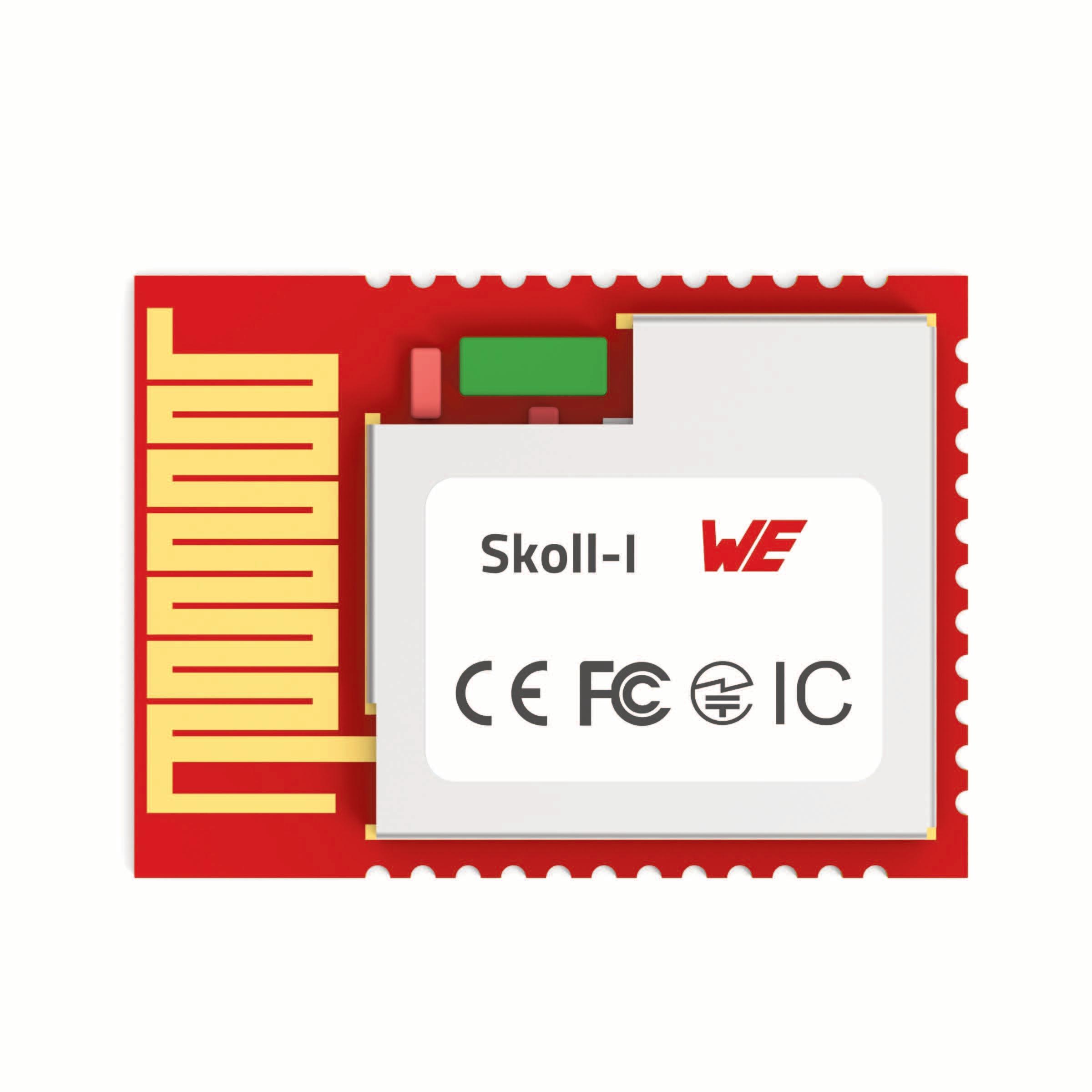
Compact and versatile: The Skoll-I wireless module combines Bluetooth® Classic und Bluetooth® LE in a compact module.
Image source: Würth Elektronik
Manufacturer of electronic and electromechanical components, introduces Skoll-I, a compact wireless module that combines both Bluetooth® Classic and Bluetooth® LE (Low Energy) version 5.4 in a single solution. Measuring just 16.6 × 12 × 1.7 mm, the module is already certified for conformity in all major target markets, accelerating the launch of new applications.
Würth Elektronik’s new Bluetooth® Classic / Bluetooth® LE module with integrated antenna is suitable for use in medical devices, industrial automation and control systems, in security technology and IoT clients such as cost-efficient predictive maintenance. These applications typically require energy-efficient operation.
Small and versatile
Combining Bluetooth® Classic and Bluetooth® LE in a compact module offers a unique opportunity for developing devices that need to connect to both legacy and modern devices. Skoll-I also offers an easy way to replace the Puck-I Bluetooth® module, which can no longer be qualified for new developments due to the withdrawal of the Bluetooth 2.0 specification. Skoll-I complies with Bluetooth® Core Specification Version 5.4 and supports BR, EDR 2/3 Mbps, Bluetooth® LE, and LE 1/2 Mbps. The module is certified to CE, FCC, IC, TELEC, and ETA-WPC standards.
Compelling all-in-one package
The WE Bluetooth® LE Terminal App provides a quick and easy way of testing as well as the basis for developing new, custom apps. Additional services include the Wireless Connectivity software development kit (SDK), the WE UART terminal, and an evaluation board that can be easily connected to a PC to provide access to all module pins for testing.
■ Würth Elektronik eiSos | www.we-online.com

Siemens’
Siemens Digital Industries Software announced that it is expanding its longstanding relationship with Arm and adding support for the newly launched Arm® Zena™ Compute Subsystems (CSS) in its PAVE360™ software, designed for software–defined vehicles (SDV).
Zena CSS, Arm’s first-generation CSS for automotive, is a pre-integrated and validated compute subsystem optimized for performance, power and area and designed to accelerate development for the AI-defined vehicle.
As the automotive industry enters a new phase of SDVs where intelligent, AI-defined functionality provides an opportunity for greater vehicle differentiation, a new development methodology and mindset is required.
“The era of AI-defined vehicles is an opportunity to bring new in-vehicle experiences to life, but it will require a much faster speed of development and deployment,” said Suraj Gajendra, vice president of automotive products and software solutions, Automotive Line of Business, Arm. “With the help of virtual platform solutions like PAVE360 from Siemens, Arm is enabling our partners to begin software development on Zena CSS before physical silicon is available, significantly reducing development time for new software solutions.”
“Our work with Arm demonstrates that it’s no longer enough that vehicle development is software defined – the process now needs to be systems-aware with the full vehicle system developed in parallel to help ensure that the entire system meets requirements and will require continuous verification,” said David Fritz, vice president, Hybrid and Virtual Systems,

Siemens Digital Industries Software. “Siemens is in a unique position to support this new approach as we enable customers to develop multi-domain (across electronics, hardware and application development) digital twin for validation and integration that encompasses the whole System-on-a-Chip (SoC), electronics/ electrical (E/E) system and vehicle development flow.”
Customers can now use Siemens’ PAVE360 to develop software for Zena CSS before silicon availability, and within the SOAFEE community, the virtual prototyping environment will become a key technology to enable SOAFEE Blueprints. . They can then functionally validate software in-system and accurately model SoC algorithms and hardware/ software interaction, helping to mitigate the inevitable challenges posed by software-defined and systems-aware vehicle development.
PAVE360™, as part of Siemens’ SDV framework, brings together the Innexis™ software environment, Veloce™ hardwareassisted verification and validation system, Teamcenter® software for Product Lifecycle, Polarion™ for Application Lifecycle Management (ALM), and Simcenter™ Prescan and Simcenter™ Amesim™ software for simulation to provide a more integrated approach to software-defined development.
The initial support for Zena CSS, based on Innexis Architecture Native Acceleration (ANA), is now available from Siemens as part of PAVE360. Automotive customers can start developing software today and, once silicon is available, continue through the PAVE360 digital twin flow seamlessly transitioning to accurate performance and power analysis using Innexis Developer Pro. In parallel, PAVE360 enables requirements and verification to be linked together providing a digital twin that is systems-aware, mitigating the inevitable system integration storm experienced by vehicle developers today.
• To learn more about how Siemens is supporting Zena CSS and enabling the automotive industry to move towards a software-defined, system-aware working methodology, visit: www.siemens.com/PAVE360blogZenaCSS
■ Siemens | www.siemens.com

Infineon collaborates with Typhoon HIL to accelerate development of xEV power electronic systems using real-time hardware-in-theloop platform
Infineon Technologies AG announced a collaboration with Typhoon HIL, a leading provider of Hardware-in-the-Loop (HIL) simulation solutions, to provide automotive engineering teams with a fully-integrated, real-time development and test environment for key elements of xEV powertrain systems. Customers working with Infineon’s AURIX™ TC3x/TC4x automotive microcontrollers (MCUs) can now use a complete HIL simulation and test solution using Typhoon’s HIL simulator for ultra-high fidelity motor drive, on-board charger, BMS, and power electronics emulation, which provides a plug-and-play interface via the Infineon TriBoard Interface Card.
The solution offered by Infineon and Typhoon HIL includes any of several Typhoon HIL Simulators for real-time digital testing, a suite of testbed hardware and software tools, and the Infineon TriBoard Interface Card, which supports Infineon AURIX TC3xx and TC4xx evaluation boards and plugs directly into a single row of DIN41612 connectors on the front panel of the HIL Simulator. The solution streamlines validation workflows, expedites design and testing processes, and reduces development costs and complexity for customers. Typhoon HIL also offers an “Automotive Communication Extender” product for its HIL Simulator solution based on an AURIX TC3xx processor, which will provide an enhanced communication interface that allows customers to connect to a larger number of heterogenous ECUs under test via CAN, CAN FD, LIN, and SPI protocols.
• The TriBoard Interface Card is available today at: www.infineon.com/cms/en/partners/design-partners/ typhoon-hil
• For more information on using Typhoon HIL’s platform with Infineon AURIX microcontrollers, visit: www.typhoon-hil.com/products/hil-interfaces/hil-infineoninterface-cards
■ Infineon Technologies | www.infineon.com

This article examines the operating principles of isolation amplifiers. It then introduces a transformerbased example that uses iCoupler technology from Analog Devices, reviews its potential applications in EV/HEV development, and presents an evaluation board to help begin the design process.

Author: Rolf Horn, Applications Engineer

Designers of electric vehicles (EVs) and hybrid electric vehicles (HEVs) need to meet the demand for higher performance, faster charging, and greater efficiency. One of the many electronic functions that can help satisfy these demands is accurate voltage sensing for optimal power control.
However, automotive applications are particularly challenging. Power electronics must function reliably for decades despite temperature extremes and the presence of high voltages that demand suitable isolation. Voltage-sensing circuits for these applica-
tions must offer high bandwidth, low error and drift, and high common-mode transient immunity (CMTI) while meeting automotive standards like AEC-Q100. These requirements are especially relevant for critical components in EVs and HEVs, including inverters, DC/DC converters, and onboard chargers.
Transformer-based isolation amplifiers are well suited to these applications. These devices use advanced technology to achieve excellent performance over decades of exposure to harsh conditions.
Operating principles of transformerbased isolation amplifiers
Isolation amplifiers are specialized differential amplifiers that provide electrical isolation between input and output circuits. This isolation can be achieved through several means, but transformerbased isolation amplifiers like the ADuM3195 (Figure 1) offer unique advantages for EV/HEV applications..
In transformer-based designs, isolation is achieved through transformer coupling. The basic principle of operation involves the following steps:
1. The input signal is converted into a high-frequency carrier signal.
2 This carrier signal is then transmitted across the isolation barrier via a transformer.
3. On the secondary side of the transformer, the original signal is reconstructed from the carrier.
The transformer serves two crucial functions. It provides galvanic isolation between input and output circuits, allowing safe measurement of high voltages and protecting sensitive circuitry. It also enables signal transfer without a direct electrical connection across the isolation barrier. Transformer-based isolation offers significant advantages for voltage-sensing applications. These amplifiers effectively reject common-mode voltages, crucial in noisy electrical environments. In addition, modern designs achieve wide bandwidths suitable for many power electronic applications.
Performance advantages of planar micro-transformers for isolation amplifiers
i Coupler, technology, developed by Analog Devices, represents an advancement in isolation amplifier design. iCoupler devices feature planar micro-transformers with a typical diameter of approximately 0.5 millimeters (mm), enabling remarkably compact solutions. The small size also provides inherent resistance to external magnetic fields, enhancing reliability.
Central to iCoupler performance is a polyimide insulation layer (Figure 2). This insulation provides high thermal and mechanical stability, making the device exceptionally durable. It can withstand surge voltages exceeding 10 kilovolts (kV) and offers long-term reliability when operating continuously at 400V root mean square (VRMS).

An essential feature of iCoupler technology is its ability to operate at high frequencies, supporting data transfers up to 150 Mbits/s (megabits per second). This is achieved in part through a highly efficient signal encoding methodology. Data is encoded into 1 nanosecond (ns) pulses that enable fast data transfer and low power consumption, typically less than 1 milliampere (mA) per channel (Figure 3).
This AEC-Q100-compliant version of the ADuM3195 is specifically designed for automotive environments. It has an isolation voltage of 3,000 VRMS, an output offset voltage of ±6 millivolts (mV) (max) at 25°C, a gain error of ±0.5% (max), a bandwidth of 210 kilohertz (kHz), a gain drift of ±27 parts per million per °C (ppm/°C) (max), and an offset drift of -22 microvolts per °C (μV/°C) (typical).

2
ADuM3195 isolation amplifier uses transformerbased isolation.
to iCoupler performance is a polyimide insulation layer that provides high thermal and mechanical stability.

Figure 3 A highly efficient encoding method allows iCoupler devices to transfer data at 150 Mbits/s and draw typically less than 1 mA per channel. ©
Additionally, iCoupler devices incorporate input glitch filters to reduce noise and ensure clean signal transmission, enhancing performance in electromagnetically noisy automotive environments.
Key features of automotive-qualified isolation amplifiers i Coupler technology has been implemented in several devices, including the ADuM3195WBRQZ isolation amplifier.
The device has a CMTI of 150 kV per microsecond (kV/μs) (typical), an operating temperature range of -40°C to 125°C, configurable gain settings, and comes in a 16-lead QSOP.
These features make the ADuM3195 WBRQZ suitable for accurate, isolated voltage measurements in challenging automotive applications, including:
• Voltage monitoring in battery management systems (BMSs)
• Feedback loops in power supplies
• Inverter and motor drive systems
The high accuracy, wide bandwidth, low power consumption, and robust isolation capabilities make the ADuM3195WBRQZ a particularly effective solution for voltage sensing in EV/HEV systems.
Isolation amplifier requirements for inverters, DC/DC converters, and onboard chargers
The ADuM3195WBRQZ isolation amplifier addresses critical challenges in EV/HEV power systems, including inverters, DC/DC converters, and onboard chargers.
Its 210 kHz bandwidth enables sub-5 μs response times, crucial for efficient charging, precise inverter control, and minimized voltage ripple in DC/DC converters. This high bandwidth also allows for smaller passive components and supports wide-bandgap device integration, enhancing overall system efficiency and power density.
The high-impedance input of the ADu M3195WBRQZ minimizes measurementrelated power loss and stabilizes converter and inverter operations. Reducing current draw also decreases stress on auxiliary circuits, improving system reliability.
The ADuM3195WBRQZ’s high temperature tolerance allows it to be placed near heat-generating components like electric motors, onboard chargers, and regenerative braking systems to help prevent thermal runaway, manage thermal cycling, and avoid hotspots in power electronics.
For DC/DC converters handling various output voltages, the ADuM3195WBRQZ’s low offset error and offset drift ensure accurate voltage feedback across temperature variations. This accuracy contributes to precise control, reduced ripple, and improved drivetrain performance.
The 3,000 VRMS isolation voltage of the ADuM3195WBRQZ protects low-voltage electronics and occupants from highvoltage systems (up to 400 V). It provides effective noise rejection between power stages and control circuits in EV battery systems while interfacing with low-voltage systems (12/48 V).
By meeting these critical requirements, the ADuM3195WBRQZ enhances the performance, efficiency, and safety of EV/HEV power systems.
It is worth noting that the ADuM4195 is available for higher voltage system requirements, providing an isolation voltage up to 5,000 VRMS and low-voltage electronics protection up to 800 V.
Jumpstart ADuM3195 development EVAL-ADuM3195EBZ (Figure 4) is a compact evaluation board designed for test
• AC measurement capability: With minor modifications, the board can measure AC voltages, which can be helpful for motor drive inverter output monitoring, AC charging system measurements, and electromagnetic interference (EMI)/noise analysis on high-voltage lines.
• Low-power option: For lower power consumption, the power disable (PDIS) input can disable the internal power supply when energy needs to be used judiciously.

Figure 4
The EVAL-ADuM3195EBZ evaluation board is designed for setup and testing of the ADuM3195.
especially relevant for EV/HEV battery systems. This allows developers to monitor battery pack voltages, measure individual cell voltages in a BMS, and interface with high-voltage DC bus lines.
• Configurable input range: The input voltage divider can be adjusted to accommodate different voltage ranges common in EV/HEV systems. For example, a 400VDC bus is typical in many EVs, 800V systems in newer EV architectures, and lower voltage ranges for 48V mild hybrid systems.
www.digikey.com


Mouser Electronics, Inc., the authorised global distributor with the newest electronic components and industrial automation products, equips engineers with the latest innovative solutions in its extensive online robotics resource centre. Combining engineering and computer science, robotics continues to drive innovation across industries, reshaping automation, manufacturing, healthcare, and more. From precisiondriven industrial systems to AIenhanced automation, robotics is redefining efficiency, safety, and performance in complex applications. Advancements in robotics span multiple domains. Soft robotics, designed to mimic organic movement, have revolutionised prosthetic development, enabling lifelike artificial limbs with enhanced dexterity. Meanwhile, sweeping robotics integrate advanced components like Time-of-Flight (ToF) sensors and antennas to optimise autonomous
cleaning. In industrial settings, robots automate repetitive and hazardous tasks, boosting productivity, while collaborative robots (cobots) optimise workflows and free human workers for strategic roles. As artificial intelligence (AI) and machine learning (ML) advance, robots are becoming smarter and more adaptable, paving the way for seamless human-robot collaboration.
Mouser’s robotics content hub provides comprehensive resources, including articles, blogs, eBooks, and products, designed to guide users through the complexities of robotics. Selecting the right robotic system is crucial to optimising performance in specific environments. Mouser’s expert technical team and trusted manufacturing partners curate technical articles and resources to help engineers identify key differences, such as automated guided vehicles (AGVs) versus autonomous mobile robots (AMRs), helping engineers navigate critical
design decisions and implement the most effective robotic solutions.
Mouser stocks the industry’s widest selection of semiconductors and electronic components, including the following products and solutions for robotics applications:
• The AD-GMSL522-SL Gigabit Multimedia Serial Link (GMSL™) robotics rapid development platform from Analog Devices, Inc.(ADI) is a GMSL-enabled NVIDIA Jetson Xavier™ NX-based carrier board and software solution that allows for simple camera-to-display conversion. This solution creates a scalable, user-friendly GMSL platform for receiving and transmitting data. The platform enables demonstrations and ecosystem development by serving as a hardware platform for software development.
• The VL53L7CH ToF sensor by ST Microelectronics is an 8×8 (64 zones) multizone sensor with an ultrawide 90° diagonal Field of View. This sensor offers a Compact and Normalised Histogram innovative output for AI applications that require multizone raw ToF sensor data. The sensor is used in cup rim detection for coffee machines and beverage dispensers, people-counting for smart buildings, and other applications like floor sensing for robotics and vacuum cleaners.
• The AEAT-901B incremental magnetic encoders by Broadcom provide an integrated solution for angular detection within a complete 360° rotation. These encoders use magnetic technology for motion control and sensing activities, which helps eliminate mechanical contact and free the device from mechanical wear and tear. The magnetic encoders feature 256 to 10,000 CPR resolution, a -40°C to 125°C operating wide temperature range, and a 5V single supply.
• The RA8E2 480MHz microcontrollers by Renesas Electronics achieve 6.39CM/MHz (CoreMarks per MHz), enabling demanding and compute-intensive applications like endpoint AI and robotics. Using the Arm® Cortex® M85 core with a 7-stage superscalar pipeline (vs. 6-stage on the CM7 core) brings an unprecedented 30% higher scalar performance, improving efficiency versus the predecessor.
To learn more, visit: https://resources.mouser.com/robotics
■ Mouser Electronics www.mouser.com

A leading automotive original equipment manufacturer (OEM), Tier 1 suppliers, semiconductor manufacturers and ecosystem partners today announced the formation of the OpenGMSL Association, an initiative bringing together industry leaders to transform SerDes transmission of video and/or high-speed data as an open, worldwide standard across the automotive ecosystem.
The demands of modern automotive systems - from ADAS (Advanced Driver Assistance Systems) to infotainment and autonomous driving - are growing rapidly.
ADAS vision systems heavily rely on high-quality video data to make critical, real-time decisions that improve driver safety and reduce accidents. Meanwhile, touchscreen infotainment systems demand high-speed, low-latency connectivity to deliver seamless, immersive user experiences.
These factors are driving up development costs for new vehicles, complicating integration, stifling innovation, and ultimately slowing advancements in safety.
With the launch of OpenGMSL Association, participation in a worldwide standard allows for innovation in autonomous driving, ADAS, and infotainment, among other applications. OEMs and suppliers can thereby accelerate time to market using solutions that operate efficiently together, thus lowering operational costs.
OpenGMSL’s standard is based on ADI’s industry-leading, road-proven Gigabit Multimedia Serial Link (GMSL) technology.
Paul Fernando, President of OpenGMSL Association, shared, “With over 1 billion GMSL ICs shipped and adoption by more than 25 global OEMs and 50 Tier-1 suppliers, GMSL is one of the most mature and roadproven high-speed video link technologies
in the automotive industry. OpenGMSL builds on this strong foundation to accelerate innovation across autonomous driving, ADAS, and next-gen infotainment - growing an already thriving ecosystem into an open, collaborative future.”
OpenGMSL Association is a non-profit entity with its own independent board of directors and encourages global participation. Products developed using the standard will require mandatory compliance testing to ensure seamless, multivendor interoperability.
For more information, please visit www.opengmsl.org. Automotive OEMs, suppliers, semiconductor manufacturers and ecosystem partners interested in joining the OpenGMSL Association can inquire at info@openGMSL.org
■ Analog Devices www.analog.com

ROHM has developed AI-equipped MCUs (AI MCUs) – ML63Q253x-NNNxx / ML63Q255x-NNNxx – that enable fault prediction and degradation forecasting using sensing data in a wide range of devices, including industrial equipment such as motors. These MCUs are the industry’s first* to independently execute both learning and inference without relying on a network connection.
As the need for efficient operation of equipment and machinery continues to grow, early failure detection and enhanced maintenance efficiency have become key challenges. Equipment manufacturers are seeking solutions that allow real-time monitoring of operational status while avoiding the drawbacks of network latency and security risks. Standard AI processing models, however, typically depend on network connectivity and high-performance CPUs, which can be costly and difficult to install.
In response, ROHM has developed groundbreaking AI MCUs that enable standalone AI learning and inference directly on the device. These network-independent solutions support early anomaly detection before equipment failure – contributing to a more stable, efficient system operation by reducing maintenance costs and the risk of line stoppages.
The new products adopt a simple 3-layer neural network algorithm to implement ROHM’s proprietary on-device AI solution “Solist-AI™.” This enables the MCUs to perform learning and inference independently, without the need for cloud or network connectivity.
AI processing models are generally classified into three types: cloud-based, edge, and endpoint AI. Cloud-based AI performs both training and inference in the cloud, while edge AI utilizes a combination of cloud and on-site systems - such as factory equipment and PLCs - connected via a network.
Typical endpoint AI conducts training in the cloud and performs inference on local devices, so network connection is still required. Furthermore, these models typically perform inference via software, necessitating the use of GPUs or high-performance CPUs.

In contrast, ROHM’s AI MCUs, although categorized as endpoint AI, can independently carry out both learning and inference through on-device learning, allowing for flexible adaptation to different installation environments and unit-to-unit variations, even within the same equipment model.
The data generated by this tool can also serve as training data for the actual AI MCU, supporting pre-implementation validation and improving inference accuracy. To facilitate adoption, ROHM has built an ecosystem in collaboration with partner companies, offering comprehensive sup-

Equipped with ROHM’s proprietary AI accelerator “AxlCORE-ODL,” these MCUs deliver approximately 1,000 times faster AI processing compared to ROHM’s conventional software-based MCUs (theoretical value at 12MHz operation), enabling realtime detection and numerical output of anomalies that “deviate from the norm”. In addition, high-speed learning (on-site) at the point of installation is possible, making them ideal for retrofitting into existing equipment.
These AI MCUs feature a 32-bit Arm® Cortex®-M0+ core, CAN FD controller, 3phase motor control PWM, and dual A/D converters, achieving a low power consumption of approximately 40mW. As such, they are ideally suited for fault prediction and anomaly detection in industrial equipment, residential facilities, and home appliances.
The lineup will consist of 16 products in different memory sizes, package types, pin counts, and packaging specifications. Mass production of 8 models in the TQFP package began sequentially in February 2025. Among these, two models with 256KB of Code Flash memory and taping packaging are available for purchase, along with an MCU evaluation board, through online distributors.
ROHM has released an AI simulation tool (Solist-AI™ Sim) on its website that allows users to evaluate the effectiveness of learning and inference prior to deploying the AI MCU.
These AI MCUs integrate a 32-bit Arm® Cortex®M0+ core (Maximum operating frequency: 48MHz) and ROHM’s proprietary AI accelerator AxlCORE-ODL that performs learning and inference using a 3-layer neural network. On top, leveraging versatile timer functions such as 3-phase motor control PWM along with a wide range of serial interfaces like CAN FD and 12-bit A/D converter enables flexible support for control and data processing in industrial equipment, residential facilities, and home appliances.
ROHM AI MCUs utilize a standard Arm® core, ensuring compatibility with commercially available tools as well as ROHM’s proprietary integrated development environment. To evaluate learning and inference, an AI operation verification simulator is provided, along with a real-time viewer for assessing AI effectiveness.

port for model development and integration. Going forward, ROHM will continue to expand this ecosystem, providing more user-friendly environments by assisting with training data creation and proposing optimal implementation methods.
Solist-AI™ is ROHM’s on-device AI solution designed for edge computing applications. Drawing inspiration from the musical term “Solist (Soloist)”, which signifies solo performance, this innovative solution enables real-time learning and inference directly on standalone edge devices without relying on cloud servers.
Powered by ROHM’s proprietary ondevice learning AI technology, Solist-AI™ is characterized by its compact design and low power consumption, contributing to the expansion of sustainable AI innovation. Solist-AI™ is a trademark or registered trademark of ROHM Co., Ltd.
Further details on the AI MCU development support system and an overview of each product can be found on ROHM’s dedicated AI MCU development system support page (below). www.rohm.com/lapis-tech/product/micon/ solistai-software
ROHM Website Resources
• Solist-AI™ Sim: PC-executable simulator for verifying AI operation
• Solist-AI™ Scope: Real-time viewer for assessing AI effectiveness (included with reference software)
• Reference Software: Sample software for AI MCUs
• Integrated Development Environment: LEXIDE-Ω (developed by ROHM)
* ROHM June 4, 2025 study on MCU products
■ ROHM Semiconductor www.rohm.com


Nowadays, embedded systems are constantly growing their memory requirements because of increasing connectivity functionality and application-level complexity. Many microcontrollers on the market provide storage density in the range of few Megabytes, which only a decade ago would have been regarded as more than sufficient and future-proof for the average application. On the other hand, integrating even more non-volatile memory requires quite a large silicon area, impacting the cost of the product significantly. A suitable alternative solution is using external memory, which can be purchased in volumes at comparably lower prices and with several densities’ options, typically starting from few to tens of Megabytes.

Author: Giancarlo Parodi, Principal Product Marketing Engineer Renesas Electronics
The external memory solution is suitable not only to hold application data but also application code, therefore removing any concern about the supplier roadmap to be able to fulfill future needs. On the other hand, some additional aspects must be taken into consideration like the performance of the code executing from the external memory, and how to protect the application code from cloning or modification. For the first problem, the solution is to use a memory with a wide interface which increases the physical throughput for the serial lines. Memories with an octal inter-
face provide one of the best choices in terms of tradeoff between the number of IO connections and the achievable 2x throughput improvement compared to the legacy quad-spi interface. Normally such modern memories also support slightly higher operating frequencies so that the performance improvement is even more significant.
Protecting the content of the memory requires usage of cryptography techniques to encrypt the code, since otherwise it would be easy for an attacker to connect to

the memory and read out the stored information with small effort. To avoid latencies for the decryption process it is necessary to use design solutions which are fast and performed in line with the instruction fetching process, in other words transparent from the CPU perspective.
The latest Renesas MCUs like the RA8x1 series implement a so-called ‘decryption on the fly’ (DOTF) architecture which serves exactly this purpose. A conceptual representation of the solution can be seen in Figure 1.

The principle is quite simple and based on the AES encryption/decryption standard, using counter mode (CTR) as specified in NIST SP800-38A. The principle of CTR mode operation is shown in Figure 2. In CTR mode, a set of counters are used as input to a block cypher function, to generate a secret output which is then exclusive-
ORed with the plaintext (or cyphertext) to encrypt (or decrypt) the message data. The sequence of counters must be chosen so that every input block in the set is different and unique.
This requirement is valid for all ‘messages’ (i.e. data items) which are encrypted using the same key.


One nice property of CTR mode is that the cypher functions associated with the counter can be performed upfront independently from each other, and do not need to wait for the data block to be available. This helps to reduce latency while reading out the encrypted data from the octa memory, since the generation of the output block can be done in parallel. Also, a certain plaintext block can be recovered independently from any other block, which is convenient for fetching program data, since depending on the program flow the processor might request to read code at non-sequential address locations.
The parameters used to define the counters need to be chosen carefully to ensure their uniqueness. An AES block is 16 bytes (128 bits) in size; therefore, the counter must be also 128 bits wide. Every encrypted block in memory is aligned to 16 bytes too, and to create a unique counter a concatenation of an initial value and the memory address can be used.
The initial value is essentially a nonce (unique, random number used once) and the address of the encrypted block being read has the 4 LSBs masked, to create the counter value according to the following scheme:
counter [127:0] = InitialValue [127:28] || (MemoryAddress [31:4] >> 4).
There are a couple of further interesting features in the implementation which are very useful to make it a flexible and userfriendly solution. First, the application can define an address boundary for which the decryption on the fly will be used, or otherwise bypassed, as shown in Figure 3.
This makes it very convenient if the application wants to partition the flash contents between code and other data, where the code gets decrypted on the fly and the data gets simply read without decrypting. The latter allows also the application to use another key or encryption mode for the data and avoids sharing the application code encryption/decryption key for multiple purposes.
As for the alignment of the DOTF area, even though the AES encryption standard implies a minimum alignment of 16 bytes, given the typical organization of a
flash memory, the boundary shall rather be placed on a sector or block size (the minimum flash unit size which can be erased while programming). In the implementation, the DOTF boundary is configurable to 4KB address alignment; in fact the application shall anyway avoid having a memory block storing both DOTF and non-DOTF data, which would make in-field-updates and factory programming unnecessarily complicated.
The flash memory device is mapped linearly into the addressable space of the MCU, and the Octa IP takes care of issuing the appropriate read commands, this is typically called XiP (execute-in-place) operation mode. For the encrypted area any access to the requested 16-byte blocks can be done efficiently by issuing one time the required address, and then reading the data continuously, thereby reducing the OctaSPI protocol overhead to a minimum.

so these can be stored safely in memory without confidentiality and integrity concerns.
The DOTF engine supports 128-, 192- and 256-bit size keys for maximum flexibility and future-proof choices, and there is no limit on the number of different keys which can be used to decrypt a specific image. The latter implies that any firmware update can use a different key if desired, and there is no need to share the same key between different MCUs.
Preparing the new image can be conveniently done offline on a secure host, before sending the image update to a device in the field or sending the encrypted image to a contract manufacturer for programming. The initial decryption key, or a “key update key” (for updating the decryption key in the field) can be injected securely in the MCU during production. Injected keys, whether in the field or at production stage, are always bound to the specific MCU, so that cloning is prevented.
Furthermore, the IP provides countermeasures to protect against side channel attacks.
All runtime operation is performed transparently by the hardware, and the provided software drivers take care to initialize and load the parameters for the DOTF operation (initial value, boundaries) and the key, before operation can start.
All MCUs which require memory expandability and complex application requirements will benefit from such kind of solution, which ensures the MCU developer will enjoy a solid application roadmap, and at the same time protect the software investment. For more information on the RA MCU family, please visit: www.renesas.com/ra.
Another important aspect is how the decryption key is handled and loaded. In devices supporting DOTF, there is a dedicated AES engine implemented within the IP but the key for the decryption process gets loaded over a private bus connection to the Renesas secure IP; this avoids leaking the key value over the internal MCU bus interconnect.
Additionally, the keys handled by the Renesas secure IP are themselves encrypted,
■ Renesas Electronics www.renesas.com


For the power designer any new technology that makes it possible to improve performance whilst simultaneously making products smaller and more energy efficient is a very exciting conceptwe’re talking holy grail territory. Over the last century the world of power electronics has witnessed many inventions and innovations and without going right back to the Thyratron, the latest major innovation was the move from analog to digital control. However, we are now witnessing a new, huge stride forwards in technology, the implementation of Wide Band Gap (WBG) semiconductors.

Author: Patrick Le Fèvre Chief Marketing and Communication PowerBox
Gallium Nitride and Silicon Carbide have been used in radio power amplifiers and high voltage diodes for years, but it was only a few years ago that they become part of the power switching chain in the form of transistors. Adopting a new technology is full of challenges that somewhat surprisingly are not always technical. Learning is an important part of the road to success but market adoption and
building a new ecosystem are far more complicated than it may seem at first. Let’s take a snapshot of where WBG currently stands and what are the remaining challenges.
The Early Adopters boosted GaN adoption!
Inevitably, for new technologies Time-toMarket is a long process, and from original


research, patenting, technology introduction and market adoption, this could be more than 10 years. We are all aware of the camel-back curve (Figure 1) and for those of us who belong to the Technology Enthusiasts category, the success of a new technology will come from the pragmatists and conservatives.
Introduced in 2005, digital control in power supplies has been broadly adopted but after 20 years it is still considered by skeptics to be a curiosity. In normal circumstances it would have been the same for the adoption of WBG, but market demand for smaller, lower power consumption, industry modernization, emerging technologies and the famous Artificial Intelligence have contributed to the speed of the learning and implementation processes.
As the Applied Power Electronics Conference (APEC) is celebrating its 40th anniversary, it is good to remind that for many technology analysts, the cornerstone of WBG took place at APEC-2018 when ‘challengers’ demonstrated the commercial potential of WBG technology.
It is not possible to name all of them but among the leaders promoting GaN I would say that the Efficient Power Conversion’s (EPC) idea to implement GaN in LiDAR was really interesting, especially with that technology becoming preponderant in the new generation of vehicles (Figure 2).
Their capacity to manage high-currents with minimal losses is paramount for enhancing accuracy and extending range in LiDAR systems. GaN's efficiency and power density advantages enable the development of smaller, lighter LiDAR systems, making it a suitable solution for

LiDAR, an acronym for “Light Detection And Ranging” is a technology that uses laser pulses to map out an environment. When the pulse contacts an object or obstacle, it reflects or bounces back to the LiDAR unit. The system then receives the pulse and calculates the distance between it and the object based on the elapsed time between emitting the pulse and receiving the return beam.
LiDAR systems are capable of processing a high volume of pulses with some systems emitting millions of pulses per second. As the returning beams are processed, the system generates a comprehensive view of the surrounding environment, enabling the use of sophisticated computer algorithms to discern shapes and identify objects such as cars and people.
Due to their high-frequency operation, which enables faster laser pulse modulation, LiDAR applications were part of the early adopter of the GaN technology.
various applications, including automotive, security, robotics, drones, and aerospace. Behind the scenes, the development of LiDAR applications has contributed to the adoption of GaN and is representing a significant volume.
2018 was also the year in which USB adapter manufacturers started to consider implementing WBG technology to offer more power in smaller packaging and to gain a competitive advantage. I mentioned EPC but Navitas Semiconductors is another example of an innovative company that in the early days pushed GaN integration to a higher level by packaging drivers and switches on the same substrate.
Making Complex Simple –
The Key to success!
When first presented, WBG power semiconductor utilization was limited by the number of drivers available, making it
difficult for power designers to consider the technology. Also, new technologies are always questioned regarding reliability and sustainability. Market adoption depends on how simple it is for power designers used to conventional MOSFETs to use WBG, and semiconductor manufacturers’ speed in developing ‘ready-touse’ solutions that include driver, protection, monitoring and many other functionalities into a single chip.
This not only simplifies implementation but also reduces the overall size of the power stage, and combined with higher switching frequencies make it possible to reduce the size of magnetics, thus increasing power density whilst reducing the overall volume and mass of the power supply.
As mentioned, among the many products that could benefit from the implementation of WBG technology, we could pinpoint portable equipment chargers. As end-users we all expect USB chargers to deliver more power, to charge faster and to be smaller and lighter.
In 2020, this wish became a reality and one example of the benefit of using WBG GaN to achieve that is a 110W Mini fast charger that is over 12 times smaller than the 96W charger supplied with the Apple MacBook Pro 16 launched by OPPO (Figure 3). This has been made possible by combining the Navitas GaNFast power ICs with a planar transformer, an optimized topology and a higher switching frequency.
At the same time, EPC released a GaN IC integrating everything to make it simple for power designers to implement into their new designs (Figure 4). Those examples illustrate how WBG GaN manufacturers rapidly moved from ‘complex’ to ‘simple’ to implement the technology, contributing to generate volume and market adoption.
High power GaN setting-up a foundation for future!
As we have seen, driven by the consumer segment, power designers soon realized the benefits offered by GaN to offer more power in smaller packaging. Power designers had to face several challenges to develop high switching frequency using GaN technology in very compact packaging but that was a really exciting time for many of us.
Presented examples addressed low and mid power applications but as well, WBG received high interest for high power applications such as Electric Vehicles (EV), renewable energy and many others.
Electric Vehicles (EV) have seen a significant uptake of WBG technology and as of today it is the dominant technology in battery chargers, power trains and as already mentioned, equipment such as LiDAR.
EV is often presented as the showcase for the adoption of WBG though less wellknown is the role of Information and Communication Technology (ICT) in supporting research on GaN and SiC.
This research aimed to develop the next generation of power supplies to support hyper-processors applications and data centers for Artificial Intelligence (AI). The rapid adoption of AI is accompanied by a


significant growth in data volume and increased computing requirements. By 2025, the data volume is projected to reach 180 zettabytes, up from 15 zettabytes in 2015. According to OpenAI researchers Dario Amodei and Danny Hernandez, the amount of computing power used for deep learning to train state-of-the-art AI models has been doubling every 3.4 months since 2012. This continuous increase in computational power directly impacts electricity consumption, with AI data centers expected to account for up to 7% of global electricity demand by 2030.
Optimizing energy utilization has always been a concern for the ICT manufacturers, requiring all suppliers, from infrastructure to components to reduce energy consumption. From the early days of research to improve the power supplies, AC/DC or DC/DC energy efficiency, power electronics designers explored new technologies and partnerships with semiconductors manufacturers.
Several papers have been presented at APEC and other conferences. It’s worth mentioning Navitas Semiconductors, who at APEC 2022 presented “Electrify Our World” introducing the benefits of WBG in ICT and, in 2024, the materialization of the utilization of that technology in power supplies for datacenters, where they predicted that power demand per unit will ultimately reach 10kW (Figure 5 insert).
Exploring the optimum benefits of combining GaN and SiC, the company released a 8.5kW, 98% efficiency reference design, complying with the with Open Compute Project (OCP), Open Rack v3 (ORv3) specifications and ready for stringent energy efficiency standards (Figure 5). This is a good representation of what has been achieved when combining WBG and other advanced technologies to power today and tomorrow ICT applications and more to be expected.
LiDAR, USB charger and ICT are representing a significant part of the market but other segments such as industrial, railway, medical are also investigating the benefits of that technology though have some concerns about the reliability and availability of new technologies.
As presented by the market analysts, despite GaN having been on the market for several years the market remains fragmented with each GaN manufacturer offering different combinations of products and services addressing specific segments.
To get the best out of GaN, power designers must work in close cooperation with semiconductor manufacturers and embrace one-stop solutions (GaN transistor, driver, protection, etc.) tightened to a single source, albeit raising concerns about the risks of using products from a
new supplier with limited history and financial background.
That, without mentioning some applications e.g., railway apps requiring 25 years lifetime and products availability for maintenance, requiring a solid and sustainable supply chain are part of complex equation when considering a new technology.
Due to that, the adoption in industrial, railway and medical applications may be slower than in EV, ICT and consumers but the obvious benefit of WBG motivated designers to explore that way.


One example is the outcome from COSEL research to combine digital control, GaN and planar magnetics that makes it possible to offer very compact power solutions that are easy to integrate into small space environments (Figure 6).
That will make it possible to house the power supply and a battery backup in the same volume as the conventional version of a similar power supply. As we are moving forwards to new applications requiring higher performances, WBG will gain market shares and follow the same path followed by the early adopters.
Many of the challenges faced by power designers when WBG technology was presented eight years ago at APEC have been overcome and there is no doubt that GaN and SiC successfully crossed the chasm. The number of applications adopting WBG will continue to grow although at the same time new disruptive technologies are reaching the market offering power designers exciting opportunities for research and development.
Starting my career within the power industry more than 40 years ago when moving from linear to switching power conversion, I crossed the chasm several times with passion and I would like to encourage young engineers to do the same, cross the chasm to approach the mythical 99.99% efficiency.
References:
Powerbox (PRBX): https://www.prbx.com
COSEL: https://en.cosel.co.jp
Navitas Semiconductor: https://navitassemi.com
Efficient Power Conversion (EPC): https://epc-co.com/epc
Applied Power Electronics Conference: https://apec-conf.org
GaN Technology – Material, Manufacturing, Devices and Design
(Edited by Maurizio Di Paolo Emilio): https://link.springer.com/book/10.1007/97 8-3-031-63238-9
■ Powerbox (PRBX) www.prbx.com
Standard off-the-shelf line of 425 W supplies are certified to IEC 60601-1 and streamline critical medical device product development
Advanced Energy Industries, Inc., a global leader in highly engineered, precision power conversion, measurement and control solutions, announced the new NCF425 series of CF-rated medical open frame AC-DC power supplies.
The system-level cardiac floating (CF) rating is the most stringent medical device electrical safety classification, with certification needed for equipment that has direct contact with the heart or bloodstream.


Advanced Energy is one of the few innovators providing standard off-the-shelf CF-rated power products. Today’s launch further expands its CF-rated portfolio, which was initially released in September 2024 with the groundbreaking release of the NCF150 series followed by the NCF250 and NCF600 series. Advanced Energy’s NCF series achieves a sub-10 μA leakage current and integrates the high levels of isolation required in critical medical devices.
“The NCF425 is the fourth in our NCF family of off-the-shelf CF-rated AC-DC power products for medical devices,” said Emdrem Tan, Advanced Energy’s Executive Vice President, System Power. “Advanced Energy offers the broadest portfolio of standard CF-rated products in the industry, with this new release offering additional options for designing critical medical systems. It helps reduce the number of isolation components needed, and minimizes system size, cost, and time to market.”
NCF425 seriesThe NCF family is designed to simplify thermal and EMI management, reduce system size and weight, and reduce the bill of materials (BOM). It also includes functionality normally provided at the system level, reducing time and complexity in the development process.
The NCF425, certified to the medical safety standard IEC 60601-1, delivers a maximum output power of 425 W in a 3.5 x 6 x 1.5-inch form factor. It also features 5 kV defibrillator pulse protection and meets the highest possible (2 x MOPP) means of patient protection rating, which requires isolation to 4 kVac and a creepage of at least 8 mm.
Applications include surgical generators, RF ablation, pulsed field ablation (PFA), cardiac assist devices and monitors, and cardiac mapping systems. For more information on the NCF425 family of CF-rated power supplies, click here
■ Advanced Energy www.advancedenergy.com

XP Power continues to make high power flexible for ease of integration across multiple platforms by extending the reach of its HPT5K0 series with the addition of 400VDC and 800VDC models. These new additions cater to engineers designing at higher voltages, including battery charging, renewable energy, and semiconductor manufacturing equipment.
All the models in the HPT5K0 series of programmable, scalable, and configurable AC-DC power supplies, which now spans from 48VDC to 800VDC, deliver 5kW of output power from a 3-phase, three-wire and earth, 180VAC to 528VAC input. This simplifies installation as there is no need for a neutral connection, which is often unavailable in industrial applications. The safety interlock feature provides enhanced safety by providing a safety-stop control that is independent of software, with signal input & outputs ready for integration with an industrial safety controller.
The HPT5K0 supports I²C, RS232 & RS485 serial buses with multiple digital protocols including PMBus™, CANopen, Modbus, and SCPI.
The ability to programme constant voltage from 0 to 105% and constant current from 0 to 110% offers design flexibility, accommodating a wide range of loads. Furthermore, the firmware can be configured through the graphical user interface (GUI), which allows for application design flexibility and tailored system integration, adapting to specific user needs.
The extensive in-built user-defined monitoring and digital controls, such as active current sharing, remote on/off, and AC/DC OK signals, contribute to an optimised system design, which can lead to reduced maintenance and operating costs, streamlining the overall efficiency of operations. Moreover, the provision of fully isolated digital communication ensures both equipment and user safety, while also enhancing the reliability of the system.
The active current sharing capability up to 25kW facilitates easy scalability, making it more straightforward to cater to higher power applications without significant redesign or investment. Additionally, achieving up to 94% efficiency in operation for reduced waste heat dissipation
helps to minimise operating costs, making the system not only effective but also economical in the long run.
Verification testing and quality controls XP Power conducts extensive verification testing and quality controls to ensure long-lasting reliability. The HPT5K0 meets EN61000-4 immunity for greater reliability in harsh electrical environments and complies with the EN55032 EMC standards for conducted (Class B) and radiated (Class A) emissions. These and industrial safety certifications help ease system integration, speeding up the process of obtaining system-level approvals.
The units are available from Avnet Abacus, Digi-Key, Distrelec, Farnell, Mouser, RS, TME, approved regional distributors, or direct from XP Power with a 3-year warranty.
• For further information about the HPT5K0 series, please visit: www.xppower.com/product/HPT5K0-Series
■ XP Power
www.xppower.com

Mouser Electronics, Inc., the authorised global distributor with the newest electronic components and industrial automation products, announces a new interactive eBook in collaboration with TDK, one of the world’s largest electronic components manufacturers, exploring the challenges of efficiency, safety, and sustainability in advanced automation applications.
Modern Industrial Technologies: Driving Efficiency and Innovation gives a deep dive into the ever-increasing demands for precision, speed, and efficiency in modern industrial automation, robotics, energy and sensor technology and how TDK’s technology portfolio empowers engineers to overcome these challenges. With TDK’s solutions already deployed across multiple industrial automation disciplines, this eBook gives insights into various considerations vital to a whole range of automation activities, from simple voltage and current measurements to complex navigational signal analysis and system diagnostics. The eBook highlights many of TDK’s products that help bridge these challenges:
The ERUC23 SMT flat wire coupled inductors feature low-loss ferrite, high-saturation currents, and low DC resistance,
offering self-leaded construction with flat wire winding and lead-free tinned terminals for 48Vinto 12Vout hybrid converters and dual-phase buck, boost, and buck-boost converters. The ERUC23 inductors also provide reduced ripple with improved efficiency in a compact package. The ERUC23 series is RoHS compatible and AEC-Q200 qualified.
The B43659 ultra-compact snap-in capacitors provide high reliability and high ripple current capability for power supplies, frequency converters, uninterruptible power supplies (UPS), medical appliances, and solar inverters. These extremely high CV products feature snap-in solder pins, an aluminium case, and both two-terminal and three-terminal versions to ensure correct installation. The B43659 series is RoHS compliant and offers a rated voltage of 450VDC and a capacitance range of 140μF to 1030μF with ±20% tolerance and operating in a -40°C to +105°C temperature range.
EPCOS / TDK’s PiezoHapt™ and PowerHap™ actuators are ideal for providing haptic feedback to user actions in smartphones and touchpad displays, car navigation systems, controllers, household appliances, industrial equipment, and medical devices. The PiezoHapt actuators consist of a vibra-
tion unit with a multilayer piezoelectric element and vibration plate, while the PowerHap version has multilayer piezo plates with copper inner electrodes. These devices are RoHS compatible and have an operating temperature range of -10°C to +60°C or -40°C to +85°C.
The FLECLEAR Ag-Stacked Film Sheets feature a thin, transparent, conductive Ag alloy layer that is deposited on a film substrate, ideal for light control windows (smart windows) and organic photovoltaics (OPVs), flexible displays and lighting, or transparent electrodes of wearable devices.
• To read the new interactive e-book, visit: https://eu.mouser.com/tdk-transformingindustries-ebook
• To learn more about all the TDK products available from Mouser, visit: https://eu.mouser.com/manufacturer/tdkcorp
• To browse Mouser’s extensive eBook library, visit: https://resources.mouser.com/manufacturer-ebooks
• For more Mouser news and our latest new product introductions, visit: https://eu.mouser.com/newsroom
■ Mouser Electronics www.mouser.com

Murata Manufacturing Co., Ltd. has launched its latest whitepaper, “Evolving Healthcare Technology: Murata’s Role in Advancing Wellness Technology.”
The paper provides insights into the Wellness and Healthcare environment, sharing how Murata’s components can support engineers in meeting challenging goals, continuing to innovate, and driving electronic-based wellness products in this space.
As wellness technologies become increasingly intelligent, wearable, and personalized, engineers face growing pressure to deliver compact, efficient, and interconnected systems. The whitepaper explores the heightened need for miniaturization, focusing on the development of smaller, lighter, and more seamlessly integrated devices that can reduce patient discomfort and enhance clinical effectiveness. It also examines the rise of medical connectivity, a critical consideration in light of the Internet of Medical Things (IoMT) and the increasing demand for continuously connected, energy-efficient devices.
The paper further considers key trends in personalized and precision medicine, highlighting the growing importance of
tailored diagnostics alongside increasing expectations for sustainability. It investigates how engineers can improve device longevity while reducing cost and environmental impact through more energy-efficient design. Available now via the Murata website, the whitepaper presents a range of component solutions designed to address these challenges:
• CELLNETTA is the world’s first metal cell fractionation filter designed to rapidly and accurately select and recover target cells from cell suspensions. Target applications include fractionation, concentration, and filtration in the development of regenerative medicine technologies or cellular pharmaceuticals.
• NeuroStoneTM is a cutting-edge 3Dprinted, interconnected ceramic technology that enables miniaturized, thermally efficient circuit assemblies. Suitable for space-constrained applications, such as implantable devices and endoscopic tools, it supports compact system design without compromising reliability.
• Microblowers are compact and lightweight air pumps capable of delivering high pressure and flow rates with mini-
mal noise. Their precise, steady airflow makes them ideal for use in ventilators, infusion pumps, and systems requiring high-accuracy drug administration.
• Stretchable Printed Circuits (SPCs) reflect the drive toward personalized, connected healthcare. These flexible, skin-conformable circuits enable realtime bio-signal monitoring and are particularly well suited to next-generation wearable devices.
• RFID Solutions support precision medicine by enabling device-level serialisation, secure pairing, and full traceability of medications and components. These features are essential for patient-specific therapies and safer, more transparent medical workflows.
• Ultra-low power Connectivity Modules form the backbone of seamless medical communication across IoMT systems. Offering robust wireless performance with extremely low energy consumption, they allow battery-powered wellness devices to operate reliably over long durations.
■ Murata www.murata.com

All-in-one electronic sensor for safety, process control, and condition monitoring
OMRON Electronic Components Europe has introduced the E8Y-L series of compact pressure displays that combine easy installation with flexible features suited to a variety of industrial process control and equipment monitoring applications.
The 31mm × 30mm × 30mm units display sensed pressure on a 3-digit, 7-segment LED panel as well as open-collector 2-output connections. Some types have a standard industrial 4-20mA analog output. Four options allow designers to select the pressure-measurement range, from 0-200Pa, 0-500Pa, 0-2kPa and 05kPa. There is also a choice of 4.5mm barb pressure port connection or a 1/8” BSPT die-cast threaded connector for standard pipe fittings, available with the two high-pressure variants.
The flexible options let these sensors monitor pressure in diverse scenarios and different zones, such as maintaining the regulated pressure in a clean room, and automatically regulating ducts or valves.
Among typical applications, the E8Y-L sensors are used in semiconductor waferprocessing reactors, to monitor organic gas-flow paths during implantation and in safety systems such as purge-gas leakage detection. Users can easily set thresholds for upper and lower limits of measurement pressure, which can simplify detecting machinery faults such as clogged exhaust or blocked vents.
Special features of the new OMRON E8YL sensors include zero-point adjustment that lets users set the zero point to any value and simplify tracking pressure changes. In addition, automatic teaching lets the user set the pressure at which the sensor turns on or off. Users interact via four simple buttons on the front panel to select the measurement range, displayed channel, and operating mode.
The sensors can operate from -10°C to 55°C with no condensation or icing, and with up to 85% relative humidity, allowing use in a wide variety of industrial environments.

With a wide supply-voltage range from 12V to 24V, and consuming up to 50mA or 75mA, the sensors are ready to operate from popular industrial power rails. In total, the new E8Y-L product line contains 13 members including all options for measurement range, output connection, and pressure port. All variants are in production now and available at distributors or OMRON online.
For further information visit: https://components.omron.com/eu-en/ products/sensors/E8Y-L
■ OMRON Corporation https://omron.eu

The automotive industry is moving toward a more sustainable future, as the industry introduces increasing numbers of hybrid- (HEV) and fully electric vehicles (EV) as well as fuel-cell operated cars. The electrification of critical functions requires reliable solutions to generate, distribute and control high-power systems. As the amount of electrical energy being stored and used by the vehicle increases, so does the need for power density and efficiency. Effective monitoring and control are essential for efficient and reliable operation of electrical subsystems.
Semiconductor suppliers like Microchip offer a broad portfolio of hardware and software, integrated development tools and high-efficiency power solutions enabled by silicon carbide (SiC) to facilitate innovation in EV and HEV systems.
Author: Andreas von Hofen, Marketing Manager - Automotive Products Group Microchip Technology
Designers of automotive subsystems constantly strive to develop innovative solutions to extend the range and reduce the charging time of EVs. In the pursuit of these goals, they have pushed siliconbased technologies close to their physical limits in terms of size, weight and power efficiency and are transitioning to SiC solutions to address these challenges. In comparison to silicon, SiC devices offer lower on-resistance, faster switching speeds, and the ability to withstand larger voltages and currents at higher junction temperatures. Another key benefit of SiC is its smaller size enables greater power density, which is critical in many key EV applications. It is not surprising that the automotive market for widebandgap (WBG) SiC power semiconductors is expected to grow thirteen times its current valuation of $1B until 2030 according Omdia (SiC power semiconductors by application, 2022 Mid Case report).
The trend towards higher voltages like 800V within EVs is driving new designs for traction-inverters, DC-DC converters, onboard chargers, and compressors for heat-pumps and fuel-cells. High-voltage SiC MOSFET’s and diode’s rugged performance are well-suited for EVs, especially in commercial and off road applications where availability is key.
The existing network of 400V charging infrastructure for the mainstream vehicles will also need to accommodate the newer 800V vehicle designs. The increasing need for high voltages is driving the development of booster DC-DC modules in the car to bring the voltage rails together.
SiC technology can also act as the switching element in a solid-state circuit breaker, or E-Fuse, to protect electric components in the vehicle and diagnose fault events before becoming a hard failure. Downtime for repairs and cost can be saved by

improved diagnosis and configuration options compared to mechanical solutions. At the same time there is demand for fast DC charging infrastructure to charge a vehicle quickly. This is particularly important for commercial applications from trucks and buses to mining and construction equipment that have to be working for as long as possible.
Using SiC for a solid-state circuit breaker brings a number of advantages compared to traditional circuit protection

solutions. The technology can switch fast using a software configurable trip profile, e. g. via a LIN interface, to interrupt a circuit in microseconds, 100–500 times faster than traditional mechanical approaches because of its high-voltage solid-state design.
The E-Fuse is resettable to avoid the need to replace physical fuses, which provides a reliable, long-term solution if a circuit is regularly interrupted. The potential risks of electric arcs when switching high voltage DC currents with mechanical contacts are eliminated when using a solidstate E-Fuse solution.
Microchip’s E-Fusetechnology demonstrator with 700V and 1200V mSiC™ MOSFET switches combines current sensing, amplifiers, LIN interface and an 8-bit PIC™ microcontroller featuring core independent peripherals to provide a complete and highly integrated solution.
All components are available with AEC automotive qualification. This design implements a Time-Current Characteristic (TCC) curve that helps designers transition from traditional fuses or contactors and is featuring a short-circuit withstand time up to 10 μs with a rated current up to 30A.
EVs, commercial and off-road vehicles require fast charging capability. While a car can sit on the driveway overnight to charge, busses or construction equipment needs to be operating effectively throughout the day or night.
These are moving to battery packs at 800V or even 1000V to provide the power levels necessary for larger vehicles with heavy hauls.
These onboard charger designs need higher levels of power where SiC technology provides an optimal solution.
A technology demonstrator of an isolated 30 kW DC-DC charger is available, based on avalanche-rated 1200V mSiC MOSFETs and 1200V dual mSiC diodes. The design is featuring >98% peak efficiency, 650–750V input voltage and 150–600V output voltage at 50–60A maximum at 140 kHz

Devices rated at voltages of 1200V and even 1700V provide developers with more design margin. This can translate into higher peak performance for the vehicle, less redundancy and easier manufacturing of elements.
The higher efficiency of SiC compared to silicon IGBTs also means smaller heatsinks are needed, reducing the weight of the vehicle.

switching frequency. The PCB layout is optimized for safety, current and mechanical stress and noise immunity.
In addition, a Three-Phase 30 kW PFC (Power Factor Correction) Reference Design in a Vienna topology is available based on SiC devices. PFCs are generally required to do the AC to DC conversion and to keep the AC input current phase shift within well-defined limits against the AC input voltage, ensuring a near-unity power factor and low total harmonic distortion (THD).
In the future, powering energy from the vehicle battery back into the grid will be a required option. This capability of bidirectional charging can be demonstrated by another 11 kW SiC-based PFC design in a Totem-Pole scheme. Both DC-DC and PFC can be combined modularly.
Building blocks for infrastructure charger up to 150 kW
Silicon carbide is also key for the charging infrastructure. The same advantages of higher voltages and currents coupled with higher efficiency for smaller cooling elements leads to smaller designs of chargers.
While the size of the charger is not as critical for commercial and off-road vehicles that are stored in a depot overnight, it is relevant for domestic bidirectional DC chargers which are gaining popularity.
Similarly public Level 3 DC fast chargers bypass the Onboard Charger (OBC) of the vehicle to directly charge the battery via the EV’s Battery Management System (BMS). Bypassing the OBC enables significantly higher charge rates, with charger output power ranging from 50 to 350 kW.
Using a modular design approach means a PFC front-end is used for the AC-DC conversion, often from higher AC voltages such as 480V, with a series of isolated DC-DC converter modules in parallel to provide the power to the vehicle.
This design approach allows a range of chargers to be developed from the basic modules to meet the different requirements of a vehicle operator. As the needs of the vehicles evolve, requiring higher power for faster charging, so the charging


infrastructure can be varied using SiC devices. This approach is being used for fast charging systems up to 150 kW and for even higher performance systems.
Using digital power management and a combination of SiC MOSFETs and diodes, enables designs that offer high-system efficiency and integration, high-power density, advanced digital control loops and increased flexibility, in various power topologies for DC fast charger applications. These can be coupled with analogue, power management, wireless and wired connectivity, energy metering, memory, security and Human Machine Interface (HMI) devices to complete a L3 DC fast charging design.
Wide bandgap solutions like SiC are key for E-Mobility, enabling higher levels of power conversion efficiency, density and reliability.
Microchip can help designers adopt Silicon Carbide with ease, speed and confidence with its mSiC™ power products and solutions. This portfolio includes SiC bare die, discretes and modules from 700V to 3.3 kV.
In addition, the overall portfolio includes MPUs, MCUs, Wi-Fi® /Bluetooth®and metering chips and the Touch Graphical Screen User Interface for applications within charging piles. On the Vehicle-side its Automotive-Grade Digital Signal Controllers, In-Vehicle-Networking components and drivers to mention a few.
The comprehensive solution also encompasses software suites for enhanced motor- and switch mode power-control algorithms, as well as automotive software stacks and diagnosis libraries for functional safety.
Microchip Technology www.microchip.com


Together with China and the USA, Europe is one of the largest sales markets for electric vehicles, which corresponded to a global share of 95% in 2023.
Experts expect 17 million new electric vehicles to be sold worldwide in 2024, representing growth of 20% compared to the previous year. For these vehicles, it is of course essential that the appropriate charging infrastructure is established in a timely manner. Rutronik, one of Europe's leading distributors of electronic components, goes one step further and sees enormous potential in public charging stations: artificial intelligence can be used to personalise the user experience, establish innovative points of sale and optimise network utilisation.
Lennart Juliusson, Business Development Manager – Business Intelligence at Rutronik, shows how this can be achieved using an EV charging station that the distributor has successfully put into operation together with the manufacturers DFI and Intel: “The future of electric vehicle charging is not just about charging the battery, but also about AI anticipating the customer's needs and enabling a seamless, personalised experience.”
Currently, the majority of charging still takes place at home with personal wall boxes or at work. According to the Federal Network Agency, there were a total of 123,449 public charging points at the beginning of 2024, including over 98,000 AC normal charging stations and
Improved user experience on the road to climate neutrality
There are over 40,000,000 electric vehicles on the world's roads - 600% more than just six years ago. Even though the economy is currently experiencing a slump in the e-mobility market segment, analysts, including those from the International Energy Agency (IEA), expect that the market penetration of electrified vehicles is yet to come - after all, they will play a key role in achieving climate neutrality across the EU by 2050.
25,000 DC fast charging stations. Across Europe, the European Alternative Fuels Observatory (EAFO) of the European Commission recorded growth of 35% in


AC normal charging stations and 75% in DC fast charging stations in 2023. This is a clear sign that fast-charging solutions are becoming significantly more important.
Challenges for customers at conventional charging stations
Until a nationwide, at least Europe-wide, standardised charging infrastructure is established, customers will be confronted with a number of “pitfalls” at charging stations: At the top of the list are technical problems, followed by software and interoperability difficulties and a lack of availability of intact or active charging points or the differences between the various providers, who each rely on individual systems. Another important point is the general user experience during the entire process, which includes the flow of information and the time required: Waiting times of one to two hours on average are unattractive for users, as this represents pointlessly wasted life time. Moreover, the user experience does not begin with the actual charging process, but before a station is even approached.
Accordingly, the developers defined a three-phase model for their demo version of the Charging Station:
• Phase 1: Pre-charging
This primarily includes personalised information on the current charging status of the vehicle transmitted to the onboard computer or smartphone via push notifications, recommendations for the optimal route to a suitable charging opportunity and the reservation of charging slots to avoid waiting times. Another feature is route planning, which serves to relieve customers' range anxiety on a longer journey with optimally placed stopovers and, depending on the stop, to offer an experience.
• Phase 2: Mid-Charging
This area is characterised by multimodular customer interaction and could include diagnostic functions networked with the vehicle, proactive troubleshooting during the charging process including the appropriate solution suggestions, as well as automated charging initiation. Other options include the implementation of a dynamic pricing model, adjustment of the charging rate and correspondingly optimised grid usage, the offering of multichannel advertising measures, social
media integration and even gamification offers to reduce waiting times.
• Phase 3: Post-charging
After charging is before charging, which is where the AI comes in and provides the customer with a comprehensive summary of the charging process or offers aftersales promotion of nearby catering and entertainment options. This service serves to build a close customer relationship and thus long-term commercial success.
Re-parking in your head: innovative design for increasing requirements
Conventional charging stations have so far been technologically reduced to the essentials: System management using a microprocessor unit (MPU) takes centre stage. Equipped with CAN and SPI interfaces for charging plugs, the power supply unit and RJ-45 connectors for the integration of an LC display, it is completely functional. The vehicle can be chargedbut nothing more.
The increasing number of e-vehicles and the associated growing demands on the charging infrastructure require a rethink in the design and layout of future-orientated charging stations.
The combination of digital signage, POS and interactive kiosk functionalities with AI applications in a charging station revolutionises their use and opens up a variety of new business opportunities. The solution, implemented by DFI, Intel and Rutronik, consolidates four different workloads and runs large voice models locally to enable real-time customer service, vehicle and behavioural analytics, fault detection and facial recognition. With three displays tailored to different needs, it generates revenue streams, increases customer loyalty, facilitates sustainability initiatives (ESG; Environmental, Social and Governance) and optimises digital operations through virtualisation technology.
On the hardware side, the developers of this charging station rely on the DFI ATX RPS630 mainboard, the 13th generation Intel Core i9 processor and the Intel Arc A380E graphics processor, which ensure smooth, trouble-free operation of the complex but clearly structured software architecture. Unlike the previous, so-called legacy designs, three virtual machines (VM) with different workflows are operated in parallel, running via a type 2 hypervisor:
1. Real-time operating system for AI-based customer service functions: The Linux operating system Ubuntu 22.04 forms the basis for this VM, which runs the AI processes for GDPR-compliant facial recognition using the Intel RealSense™ camera and speech recognition based on OpenAI Whisper. An AI chatbot is also integrated here, which uses Mistral 7B, an open source large language model (LLM) that can process longer input sequences better than alternative models. Intel is also contributing OpenVINO™, an open source toolkit that accelerates AI inference with lower latency and higher throughput, while maintaining accuracy, reducing the model footprint and optimising hardware usage. It streamlines AI development and the integration of deep learning in areas such as computer vision, large language models (LLM) and generative AI. The PyTorch model includes the definition for different models and includes the definition for different tasks, such as in this case image classification, pixel segmentation, or playback quality of videos and also serves to reduce latency. Combined with high-quality microphones, loudspeakers and a 10.1" sound monitor, the interaction between the Charging Station and users becomes significantly more efficient and intuitive, which considerably improves the user experience.
2 Advertising placements:
This VM contains the content management system for personalised advertising measures and works with a Windows 10 operating system. A 21.5" display, for example, ensures optimum presentation.
3 Kiosk:
The Charging Station Demo utilises the entire available area of the display and also integrates the rear for the multipurpose approach. A 32" screen makes it easy to improve the mid- and post-charging process by integrating social media, gamification or after-sales promotion. This VM also runs on Ubuntu.
The user experience “behind the scenes” is also taken care of in the new design: thanks to an integrated module for outof-band management, it is possible to reactivate a charging station that has been completely switched off using remote maintenance. This eliminates unnecessary journeys and reduces maintenance and servicing costs.
As the system relies on workload consolidation, whereby multiple tasks are compressed onto fewer platforms, there is no need to integrate a separate board for each operation, which reduces overall system costs. Thanks to the integration of three VMs, it is also possible to keep the station online almost continuously, as system repairs or maintenance work can be carried out in the background.
Charging stations designed in this way offer endless options for further development, e.g. for nationwide, embedded smart city applications that are significantly less susceptible to interference than previous
offerings. As the system complies with various communication standards, it is already Wi-Fi or 6G-capable for future extended applications. Thanks to the hardware concept used and the integration of various security standards, the station also forms a closed system, which massively increases security in terms of payment processing and data protection.
It is also possible, for example, not to switch the camera on all the time, but to couple it with an infrared sensor so that facial recognition only starts when a user is within a defined area. The reinforced screens also ensure sufficient security against vandalism and other external influences.

A Europe-wide regulation on the expansion of the infrastructure for alternative fuels (Alternative Fuels Infrastructure Regulation, AFIR) came into force on 13 April 2024. The aim of this regulation is to standardise the design of charging stations and simplify the charging process for customers, thereby placing a strong obligation on charging station operators.
The aim is to avoid the inefficient, unecological and inconvenient search for the right charging station - in short, to improve the user experience for e-vehicle drivers in order to make the switch to emobility more attractive. Another area of the regulation stipulates that fast-charging infrastructure is to be installed at regular intervals on all major European roads. These measures are intended to counteract the notorious (German) range and availability anxiety and normalise charging processes.
The solution presented takes this regulation one step further by placing the user at the centre of the charging process, while at the same time using its analysis capabilities to stabilise the power grid. A vehicle that is known not to be driven for at least the next three hours because the driver is visiting a nearby exhibition or a recommended restaurant can be charged more slowly.
Rutronik acts as a reliable distribution partner that understands the needs of both original equipment manufacturers (OEMs) and manufacturers, can provide the right solutions and is involved from component selection to design-in. The extensive line card, coupled with the complementary expertise of the Rutronik product managers, creates the best fit for the customer.
Thanks to the extensive experience gained from its own research and development work as part of Rutronik System Solutions, Rutronik understands all the more what developers need and how to get it.
■ Rutronik www.rutronik.com


Authors:
Richard Anslow, Senior Manager, Analog Devices
Danail Baylov, Staff Engineer, Analog Devices
There are multiple approaches to adding more intelligence to industrial systems, including edge and cloud artificial intelligence (AI) matched to sensors with analog and digital components. With the diversity of AI approaches, the sensor designer needs to consider several competing requirements, including latency for decision-making, network usage, power consumption/battery life, and AI models fit for machines. This article series focuses on the design of an intelligent AI wireless motor monitoring sensor, and answers key questions such as how can edge AI extend the sensor battery life? And what is the improvement in my system insights and decision-making? The sensor presented uses an edge AI algorithm to detect anomalous motor behavior, triggering machine diagnostics and maintenance, and enabling longer motor operating life.
Condition-based monitoring (CbM) of robotics and rotating machines, such as turbines, fans, pumps, and motors, records real-time data related to the health and performance of the machine to enable targeted predictive maintenance, as well as optimized control. Targeted predictive maintenance, early in the machine life cycle, reduces the risk of production downtime resulting in increased reliability, significant cost savings, and increased productivity on the factory floor. CbM of industrial machines can utilize a range of sensor data, such as electrical measurements, vibration, temperature, oil quality, acoustic, magnetic, and process measurements such as flow and pressure. However, vibration measurement is the most common by far, as it can provide the most reliable
indication of mechanical issues such as imbalance and bearing failure. This article introduces the Voyager4 evaluation kit (EV-CBM-VOYAGER4-1Z), a robust, low power, wireless vibration monitoring platform that enables designers to rapidly deploy a wireless solution to a machine or test setup. The Voyager4 sensor uses an edge artificial intelligence (AI) algorithm to detect anomalous motor behavior, triggering machine diagnostics and maintenance, and enabling longer motor operating life. This is Part 1 of a series of three articles documenting the Voyager4 sensor, which can be used as a template to accelerate design efforts and understand tradeoffs in intelligent system design.
• Part 1 of this article series will introduce the Voyager4 wireless condition monitoring sensor, including key elements of sensor architecture, hardware design, power profiling, and mechanical integration.
• Part 2 of this article series will focus on the software architecture and AI algorithm. A complete system-level approach for AI model development and deployment on the Voyager4 is described.
• Part 3 of this article series will look at the practical implementation of the AI algorithm and the different faults Voyager4 can detect such as imbalance, misalignment, and bearing defects.
Wireless industrial sensors currently available on the market typically operate on very low duty cycles. The user sets the sensor sleep duration, after which the sensor wakes up and measures temperature and vibration, and then sends the data over the

radio back to the user’s data aggregator. Commercially available sensors typically quote a 5-year battery life, based on one data capture per 24 hours, or multiple data captures per 24 hours. See Figure 1. In most cases, sensors operate in sleep mode more than 90% of the time. The Voyager4 sensor will operate in a similar fashion but take advantage of edge AI anomaly detection (using the MAX78000 AI microcontroller) to limit the use of the radio. When the sensor wakes up and measures data, the data is only sent back to the user if the microcontroller detects an anomaly in the data. By using AI at the edge, the battery life can be increased by at least 50% (see the Hardware System and Power Profiling section).

© ADI Figure 1
Industrial wireless sensor typical operation.
The Voyager4 sensor principle of operation is shown in Figure 2. The ADXL382 triaxial 8 kHz digital micro electronic mechanical systems (MEMS) is used to gather vibration data. First, the raw vibration data follows Path A to the MAX32666 Bluetooth® low energy (BLE) processor.
The data can be sent to the user over BLE radio, or via USB. This raw vibration data is used to train an edge AI algorithm using MAX78000 tools
Using the MAX78000 tools, the AI model is synthesized into C code. The edge AI algorithm is sent in a BLE over-the-air (OTA) update to the Voyager4 sensor and stored in memory using the MAX78000 processor with edge AI hardware accelerator.

After this initial Voyager4 training phase, the ADXL382 MEMS data can follow Path B shown in Figure 2.
However, if faulty vibration data is predicted, then Path C is followed, with a vibration anomaly alert sent to the user over BLE. Part 2 of this article series will explain this edge AI implementation in more detail.
Hardware System and Power Profiling Figure 3 provides an overview of the Voyager4 hardware system. The ADXL382 is a low noise density, low power, 3-axis MEMS accelerometer with selectable measurement ranges. The device supports ±15 g, ±30 g, and ±60 g ranges and a wide 8 kHz measurement bandwidth. The ADG1634 single-pole double-throw (SPDT) CMOS switch is used to route the MEMS raw vibration data to either the MAX32666 BLE radio or the MAX78000 AI microcontroller. The BLE microcontroller is used to control the SPDT switch. Several other peripherals are wired to the MAX32666, including a MAX17262 fuel gauge used to monitor battery current, and an ultra low power ADXL367 MEMS accelerometer. The ADXL367 is used to wake up the BLE radio from Deep Sleep mode in a high vibration shock event. It consumes only 180 nA of current in motion-activated wake-up mode. The BLE microcontroller can stream the ADXL382 MEMS raw data to the host using either BLE or USB using the FTDI FT234XD-R.

The MAX78000 edge AI algorithm will predict faulty or healthy machine operation based on the vibration data gathered. If the vibration data is healthy, then there is no need to use the MAX32666 radio. The Voyager4 sensor operation can follow Path D shown in Figure 2, where the MEMS returns to sleep mode.
The Voyager4 sensor uses the MAX20335 power management integrated circuit (PMIC), as shown in figures 3 and 4. The PMIC features two ultralow quiescent current buck regulators and three ultralow quiescent current low dropout (LDO) linear regulators. Each LDO and buck regulator output voltage can be individually enabled and disabled, and each output voltage value can be programmed through I2C with the default preconfigured. The BLE processor is used to enable or disable individual PMIC power outputs for different Voyager4 operating modes. The different Voyager4 sensor operating modes are detailed in Table 1.
Output ON, 0 = Output OFF
Table 1: Voyager4 Sensor Operating Modes and Corresponding MAX20335 PMIC Power Configuration
Table 2 provides a breakdown of features based on the MAX32666 and MAX78000 active or inactive modes. For example, for training mode, the BLE microcontroller


must first advertise its presence in the BLE network and then make a BLE connection with the network manager. The Voyager4 then streams the ADXL382 MEMS raw data over the BLE network for training an AI algorithm on the user’s PC. Then the Voyager4 sensor returns to a Deep Sleep mode. In Normal (AI) mode, the BLE radio advertising, connection, and streaming features are disabled by default. At periodic intervals, the MAX78000 wakes up and runs an AI inference. If no anomaly is detected the Voyager4 returns to Deep Sleep mode. The Voyager4 evaluation kit is characterized for average power consumption based on the time between events for the Deep Sleep, Training, and Normal/AI modes. Figure 5 shows a summary of the average power consumption.
The Voyager4 evaluation kit (EV-CBM-VOYAGER4-1Z) includes several components (LEDs, pull-up resistors) used for customer evaluation convenience. These contribute to the 0.3 mW Deep Sleep current on the LDO1OUT voltage rail, as illustrated in Figure 5. When the evaluation kit operates in training mode, over 0.65 mW of power is consumed when the BLE is active, advertising, connecting, and transmitting data once per hour. If the Voyager4 sensor operates in AI mode the power consumption is closer to 0.3 mW, even when the sensor is active once per hour.

The Voyager4 sensor measures 46 mm in diameter, and 77 mm minimum height, with an M6 threaded hole in the base for a screw stud or adhesive mount to a motor casing. Figure 6 provides an exploded view of the mechanical assembly with an aluminum base and wall housing, and an ABS plastic lid to mitigate against antenna shielding for BLE data transmission. The BLE and edge AI microcontroller PCB is vertically mounted with a battery attached to a standoff. The MEMS sensor and power PCB is placed on the base, close to the monitored vibration source.

A well-constructed mechanical enclosure design for a MEMS accelerometer will ensure that high quality vibration data for CbM is extracted from the monitored asset. Designing a good mechanical enclosure requires an understanding of modal analysis.
For vibration sensors, the natural frequencies of the enclosure must be greater than that of the applied vibration load measured by the MEMS sensor. For Voyager4, the 3 dB bandwidth across the X, Y, and Z axes is 8 kHz. The sensor enclosures should not have any significant resonances at less than 8 kHz.
ANSYS and other simulation tools provide modal analysis plugins, which enable the designer to explore the effect of geometry, material selection, and mechanical assembly on the frequency response of the sensor enclosure. The sensor enclosure mass, stiffness, and natural frequencies are interrelated. The mass matrix [M], stiffness matrix [K], angular frequency ωi, and mode shape {∅i} are related by Equation 1 used in FEM programs like ANSYS. The natural frequency fi is calculated by dividing ωi by 2π, and the mode shape {∅i} provides the relative deformation patterns of the material at specific natural frequencies.

For a single degree of freedom system, the frequency is simply expressed by Equation 2.

Figure 5 shows that a sensor, which does not have to transmit raw BLE data, can consume up to 50% less power. At approximately 0.3 mW power consumption, up to two years battery life is possible with one 1500 mAh battery (for example, using TinyCircuits’ rechargeable ASR00073), or over 7 years if using two standard AA size 2.6 Ah LS14500 Saft batteries. Saft’s LS 14500 cell is ideally suited for long-term applications (typically from 5 to 20+ years), featuring low base currents and periodic pulses.
Modal analysis is used to understand the vibration characteristics of structures. It provides the natural frequencies and normal modes (relative deformation) of a design. The primary concern in modal analysis is to avoid resonance, where the natural frequencies of a structural design closely match that of the applied vibration load.
Equation 2 provides a simple intuitive way to evaluate a design. As you reduce the height of the sensor enclosure, the stiffness increases and the mass decreases, therefore the natural frequency increases. Also, as you increase the height of the enclosure, the stiffness reduces and the mass increases, resulting in a lower natural frequency. Most designs have multiple degrees of freedom. Some designs have hundreds. Using the finite element method provides quick calculations for Equation 2, which would be very time-consuming to do by hand. Using simulation tools and equations 1 and 2, along with careful material selection ensures that the design meets frequency response targets. The article “How to Design a Good Vibration Sensor Enclosure Using Modal Analysis” provides a complete overview of modal analysis for further reading.
The mode participation factor (MPF) is used to determine which modes and natural frequencies are the most important for your design.
The mode shape {∅i}, mass matrix [M], and excitation direction vector D are related by Equation 3 MPF. The square of the participation factor is the effective mass.

The MPF and effective mass measure the amount of mass moving in each direction for each mode. A high value in a direction means the mode will be excited by forces, such as vibration, in that direction. To complete the interpretation of modal analysis, it’s important to understand that all points on a structure vibrate at the same frequency (global variable), but the amplitude of vibration (or mode shape) at each point is different.
For example, an 18 kHz frequency can affect the top of the mechanical enclosure more than the bottom.
The Voyager4 sensor assembly was simulated using 3003 aluminium alloy for the enclosure bottom, mid-section, and ABSPC plastic for the lid.
The modal analysis simulation results are shown in Table 3, with a total of 14 mode results captured in the frequency of interest. The MPFs in the X, Y, and Z directions are tabulated. The strongest modes are highlighted in blue. The simulation results are used to examine the deformation locations for these relatively strong modes.
Modes 1 and 2 are similar and affect the ABS-PC lid as shown in Figure 7. Based on the location of Mode 1, far away from the sensor PCB located at the base,
it is predicted that this small resonance should not affect the ADXL382 MEMS performance. Mode 7 is also highlighted in Table 3. This occurs at approximately 7.25 kHz on the Z (vertical) axis. Figure 8 shows some appreciable effects on the vertical wall of the enclosure. However, the base is not strongly affected by Mode 7.
Mass Participation (Normalized)
Table 3: Modal Analysis Simulation Results


This modal simulation shows that there are no modes that will have an appreciable effect on the ADXL382 sensor PCB located on the enclosure base, and the 3 dB, 8 kHz bandwidth of interest should not have significant mechanical resonances.
To validate the simulation results, the Voyager4 sensor was placed on a modal shaker, with a constant 0.25 peak (g) input vibration, and frequency sweep from 0 kHz to 8 kHz. The frequency response of the Voyager4 sensors is within ±1.5 dB up to 8 kHz as shown in Figure 9.
Microcontrollers with embedded AI hardware accelerators provide a path to better decision-making and longer battery life for wireless sensor nodes. By using AI at the edge, the battery life can be increased by at least 50%. Modal analysis for vibration sensor enclosures accelerates the sensor development cycle and ensures good quality vibration data captured from monitored assets.
■ Analog Devices www.analog.com

Engage with like-minded members and ADI technology experts in our online community, EngineerZone®. Expand your network, ask your tough design questions, share your expertise, browse our rich knowledge base, or read about new technologies and the engineers behind them in one of our blogs. Visit https://ez.analog.com


Author: Hermann Reiter, Senior Director, Supplier Business Development
As technological advancement rapidly propels us forward, the pressure to build a more sustainable future has never been greater. The road to a greener tomorrow is filled with environmental and logistical challenges that require a unified approach across manufacturers, distributors and supply chains to create effective new approaches and systems.
Traditional manufacturing models are known for prioritizing efficiency over sustainability – and being resource-intensive. A truly sustainable future demands a paradigm shift. Flexible manufacturing systems offer a promising path forward.
As technological advancement rapidly propels us forward, the pressure to build a more sustainable future has never been greater. The road to a greener tomorrow is filled with environmental and logistical challenges that require a unified approach across manufacturers, distributors and supply chains to create effective new approaches and systems.
By embracing adaptability and agility, manufacturers can reduce waste, optimize resource utilization and start adopting principles of circularity where resources are continuously recycled and reused. While there is still much work to be done, many leaders and companies in the manufacturing industry are already collaborating and using their innovative technologies to leverage data, analytics and automation to help customers make more informed decisions, choose smarter products, implement sustainable practices, reduce greenhouse emissions and more. As a leading global electronic components distributor, along with several of our supplier partners, DigiKey has firsthand insight into the positive impact of
the digitalization movement and how it’s helping reduce everything from energy use to water consumption, inefficient labor hours and excessive costs in manufacturing facilities across sectors.
The European Imperative: Prioritizing a Sustainable Future
While the global manufacturing industry is gaining significant momentum on sustainability goals, European leaders and government officials are leading the charge. The European Union aims to be an economy with net-zero greenhouse gas emissions. Parliament adopted the EU Climate Law in June 2021 to reduce emissions by 55% by 2030 and climate neutrality by 2050.
These ambitious targets necessitate a fundamental shift across all sectors of the economy, with manufacturing playing a pivotal role.
While the pressure to decarbonize has been high, the European Union is on the road to streamlining and simplifying its sustainability rules, such as reporting requirements and compliance deadlines, for corporations through a new proposed omnibus regulation. If approved, the goal is to reduce administrative and reporting burdens on companies and unlock more business investment in sustainability efforts,
With important drivers in place, the shift to flexible manufacturing is positively impacting sustainability and efficiency efforts.
One DigiKey supplier – Analog Devices Inc. (ADI), a global semiconductor leader in security, AV and low-voltage products – is seeing this impact. ADI customers are investing in adaptable manufacturing within their own plants.
This enables production lines to be changed quickly when necessary, building capabilities to react faster to different regional requirements.
• Optimize resource utilization: Updating production lines to incorporate renewable energy sources, optimizing material usage, and minimizing energy consumption can have strong benefits. I recently visited Schneider Electric, which is treating its wastewater to produce hydrogen and cut CO2 emissions. They are also using solar panels to generate electricity – all of which are impressive efforts to drive change.
Digital technologies are crucial to sustainable manufacturing.

We know meeting sustainability targets requires a holistic approach, meaning “everybody is in scope” – calling for every individual, department and process within an organization to contribute to the sustainability journey.
According to the 2023 IDC Global Sustainability Readiness Survey, 45% of EMEA manufacturers noted sustainabilityrelated requirements from business partners were a top driver for operationalizing sustainability, followed by mitigating risks associated with non-sustainable operations and improving brand reputation.
Flexible manufacturing is a production method that allows manufacturers to quickly pivot with changes in product demand. It uses automation to manage production processes and can enable the following outcomes:
• Reduce waste: By responding quickly to changing market demands and minimizing overproduction, manufacturers can reduce material waste and lower environmental impact. For example, if battery longevity in the electronics market can be improved, products like mobile phones can last longer or be more readily recycled.
Digital signals are data points generated by sensors and machines in a factory.
These signals are then converted into a digital format to be analyzed and used to monitor, control and optimize production processes, provide real-time insights and improve efficiency levels. Reports generated by connected solutions can indicate machine status, product quality, material levels and other measures in real-time through embedded vision systems. This allows for better quality control, predictive maintenance scheduling and overall process efficiency.

By connecting digital signals and data across the value chain, manufacturers can gain valuable insights into their environmental footprint. An example is a smart dust collector in a manufacturing facility that provides real-time updates on airflow quality, differential pressure and production runs from a single dashboard.
Engineering a More Sustainable Future: Logistics as a Lever
When considering how to optimize operations, it’s fundamental to begin by looking at material flow, industrial vision and automated robotic systems – key areas that are helping move the industry toward a more sustainable future.
Optimizing material flow within and between facilities minimizes transportation distances, reduces fuel consumption and lowers emissions. For example, ADI is implementing a net-zero warehouse to equalize energy from renewable sources as it consumes them. In our warehouses, DigiKey uses automation to increase productivity, utilize space better and maintain inventory accuracy in our distribution center. We also bundle orders to save on
packaging, space and freight costs when shipping products. Every sustainable action or practice put into action adds up from an environmental perspective.
Another area driving sustainable manufacturing innovation is automated robotic systems that improve warehouse efficiency, reduce labor costs, lower the risk of errors and minimize the environmental impact of transportation. Vision systems are also optimizing warehouse operations and improving inventory management.
Managing logistics can be complex, but using them to support your company’s sustainability plan can result in significant ROI and increase long-term profitability.
The path to a more sustainable future is challenging, but by taking key steps, it is within reach. By embracing innovation, fostering collaboration and recognizing the responsibility of “everybody in scope,” European organizations have taken steps to lead and inspire a global movement toward a more sustainable and prosperous future.
However, it takes a collective effort. Governments, businesses and individuals must work together to drive innovation and accelerate the transition to a low-carbon economy.
At DigiKey, we understand the importance of having the right products and components available to help connect our industry and customer base on their quest to build a more sustainable world for generations to come.
Learn more about our work and partnerships by watching our new Sustainable Futures video series.
DigiKey is recognized as the global leader and continuous innovator in the cuttingedge commerce distribution of electronic components and automation products worldwide, providing more than 15.9 million components from over 3,000 quality name-brand manufacturers.
■ DigiKey www.digikey.com


Most of the global internet traffic, which is growing due to AI and data centres, is routed via more than 400 submarine cables. These form the main artery of the international network, spanning around 1.2 million km.

Author: Tomohide Yamazaki, Ph.D Assistant Manager, Anritsu
A typical submarine optical cable system comprises the optical fibre cable, repeater, and beach manhole to connect the submarine and land cables, as well as the cable landing station, a dedicated facility for pulling up submarine cables that house power supply, monitoring, and circuit-termination equipment. The repeater functions encompass optical amplification using an Erbium-Doped Fibre Amplifier (EDFA), point-of-failure monitoring, and optical distribution function.
The subsea portion from the beach manhole is called the wet plant and the portion on land is called the dry plant.
Recently, there has been a trend towards increasing use of the open-cable model, where the wet and dry plants are operated by separate communications providers, clarifying the demarcation points of responsibility at the beach manhole. Submarine cables typically remain in service for 25 years or longer, but the cable landing station is upgraded frequently as technology advances.
Submarine cable testing requirements
Signal transmission loss and the repeater operation are monitored when ultralongdistance submarine cables are deployed. However, since the cables can also be damaged by ship anchors or natural dis-

asters, identifying the exact failure location is important before incurring the costs of pulling up and repairing cables.
A C-OTDR (Coherent Optical Time Domain Reflectometer) with heterodyne detection is considered the best instrument to accurately detect location faults in an optical submarine cable over ultralong distances. The C-OTDR detects the Rayleigh backscatter light caused by impurities inherent in the optical fibre, like a common OTDR. The EDFAs installed on repeater systems used on submarine cables can only amplify optical signals in the transmission direction. This means that the backscattered light in the EDFA can’t be returned to its original path.

Instead, submarine cables incorporate optical fibre return paths that connect the uplink and downlink EDFA outputs –enabling the C-OTDR to detect all backscattered light ahead of the repeater to identify faults.
The C-OTDR uses the same basic principles of a common OTDR, which transmits light into the optical fibre and then detects the
reflections (or backscatter) from the fibre under test. The light emitted from the laser source is split into two optical paths using an optical coupler. In one path, the light is converted to pulsed light by an A/O modulator and injected into the submarine optical cable.
The most important function of the COTDR is coherent detection, which is a method of re-injecting the original transmitted wavelength so that the test result only shows information at exactly that wavelength. Although each amplifier used in a submarine network to boost

The light in the other path, designated the local oscillator (LO), is combined with the backscattered light returning from the fibre under test. Before the combination, the backscattered light is filtered to remove the active DWDM (Dense Wavelength Division Multiplexing) signals as well as extra noise.
The C-OTDR measures and calculates the power of the beat light, which is the interference light between the two, and displays the measured waveform on the screen.
optical power also increases the Amplified Spontaneous Emission (ASE) noise power, the coherent detection method enables the C-OTDR to detect the backscattered light below the ASE noise. The C-OTDR can also adjust the wavelength of the pulsed light injected into the submarine cable, enabling the test of practical DWDM wavelengths.
In a common live network system, the input optical power to an EDFA is flat across the DWDM wavelengths. On the other hand, C-OTDR is often used on the no-traffic (no-optical signal) system.

In this system, the EDFA gain control cannot maintain a stable output due to the pulsed light generated by the C-OTDR. To address this, the C-OTDR outputs a probe and dummy light to ensure a constant optical power input to the EDFA.
A submarine network consists of optical fibre pairs comprising an uplink and downlink, which are connected via the optical return path at each repeater. As backscattered light is returned only in the

The C-OTDR probe and dummy light are normally placed as far away from the active DWDM wavelengths, minimising any chance of interference between the C-OTDR light and DWDM signals.
opposite direction to the transmission signal, testing for the true fault location must be done in the same direction as the transmission link optical fibre (transmitter side).

If either the uplink or downlink cable is broken (i.e. A to B but not B to A), testing from the receiver end side, the fault will show the end location of the repeater directly following the cut location.
As a result, the location could be inaccurate by as much as the distance of the repeater sections (up to 90 km). This is because the C-OTDR only ’sees’ backscatter light propagated towards the receiver from the repeater after the cut.
A major cause of optical fibre cuts is due to seabed movement. This movement can cover a large geographical area and affect a large section of cable. When a cable is broken in two locations, fully understanding this situation is very important.
To help engineers locate optical submarine cable faults, Anritsu offers the Coherent OTDR MW90010B, which can measure ultra-long submarine cables of up to 20,000 km with a 10 m resolution and with optical-amplifier repeaters separated by distances of 80 km or more.
Using coherent detection, the MW90010B evaluates fault location, cable and bending loss, fibre length, and so on. Setting the built-in tunable light source with a wavelength accuracy of ±0.05 nm to a wavelength range of 1527.60 to 1567.13 nm supports the testing of the DWDM submarine cables.
C-OTDR offers the best technology for testing submarine fibre optical cables. Newer generation instruments enable extremely accurate distance measurements as well as full characterisation of optical events.
Combining C-OTDR coherent technology and the submarine cable feedback path ensures thousands of km of fibre can be characterised quickly and efficiently.

