https://ebookmass.com/product/wide-bandgap-semiconductorpower-devices_-materials-physics-design-and-applications-b-
Instant digital products (PDF, ePub, MOBI) ready for you
Download now and discover formats that fit your needs...
The IGBT Device: Physics, Design and Applications of the Insulated Gate Bipolar Transistor 2nd Edition B. Jayant Baliga
https://ebookmass.com/product/the-igbt-device-physics-design-andapplications-of-the-insulated-gate-bipolar-transistor-2nd-edition-bjayant-baliga/ ebookmass.com
Quantum Physics of Semiconductor Materials and Devices Debdeep Jena
https://ebookmass.com/product/quantum-physics-of-semiconductormaterials-and-devices-debdeep-jena/
ebookmass.com
Pyroelectric Materials : Physics and Applications Ashim Kumar Bain
https://ebookmass.com/product/pyroelectric-materials-physics-andapplications-ashim-kumar-bain/
ebookmass.com
Orpheus: A Greek Mythology Gay Retelling (Book 3 of the Mythologay Series) B.J. Irons
https://ebookmass.com/product/orpheus-a-greek-mythology-gay-retellingbook-3-of-the-mythologay-series-b-j-irons/
ebookmass.com
Experimental Film and Photochemical Practices Kim Knowles https://ebookmass.com/product/experimental-film-and-photochemicalpractices-kim-knowles/
ebookmass.com
Train Me Daddy: An Age Play Mafia Daddy Romance (Mafia Daddies NYC Book 1) Zack Wish
https://ebookmass.com/product/train-me-daddy-an-age-play-mafia-daddyromance-mafia-daddies-nyc-book-1-zack-wish/
ebookmass.com
Where Did the Universe Come From? And Other Cosmic Questions Ferrie Chris
https://ebookmass.com/product/where-did-the-universe-come-from-andother-cosmic-questions-ferrie-chris/
ebookmass.com
Essential C# 12.0, 8th Edition Mark Michaelis
https://ebookmass.com/product/essential-c-12-0-8th-edition-markmichaelis/
ebookmass.com
Sustainable Alternatives for Aviation Fuels Abu Yousuf
https://ebookmass.com/product/sustainable-alternatives-for-aviationfuels-abu-yousuf/
ebookmass.com
Enhancing Student Support in Higher Education: A SubjectFocused Approach 1st Edition Nick Pilcher
https://ebookmass.com/product/enhancing-student-support-in-highereducation-a-subject-focused-approach-1st-edition-nick-pilcher/
ebookmass.com
WideBandgapSemiconductorPowerDevices RelatedTitles TheIGBTDevice:Physics,DesignandApplicationsoftheInsulatedGateBipolarTransistor (ISBN978-1-4557-3143-5)
PowerElectronicsHandbook,ThirdEdition (ISBN978-0-12-382036-5)
WideBandgapPowerSemiconductorPackaging:Materials,Components,andReliability (ISBN978-0-08-102094-4)
WideBandgap SemiconductorPower Devices Materials,Physics,Design, andApplications Editedby
B.JayantBaliga
WoodheadPublishingisanimprintofElsevier
TheOfficers’MessBusinessCentre,RoystonRoad,Duxford,CB224QH,UnitedKingdom
50HampshireStreet,5thFloor,Cambridge,MA02139,UnitedStates
TheBoulevard,LangfordLane,Kidlington,OX51GB,UnitedKingdom
Copyright © 2019ElsevierLtd.Allrightsreserved.
Nopartofthispublicationmaybereproducedortransmittedinanyformorbyanymeans,electronicor mechanical,includingphotocopying,recording,oranyinformationstorageandretrievalsystem,without permissioninwritingfromthepublisher.Detailsonhowtoseekpermission,furtherinformationaboutthe Publisher’spermissionspoliciesandourarrangementswithorganizationssuchastheCopyrightClearance CenterandtheCopyrightLicensingAgency,canbefoundatourwebsite: www.elsevier.com/permissions.
ThisbookandtheindividualcontributionscontainedinitareprotectedundercopyrightbythePublisher (otherthanasmaybenotedherein).
Notices
Knowledgeandbestpracticeinthisfieldareconstantlychanging.Asnewresearchandexperiencebroadenour understanding,changesinresearchmethods,professionalpractices,ormedicaltreatmentmaybecome necessary.
Practitionersandresearchersmustalwaysrelyontheirownexperienceandknowledgeinevaluatingandusing anyinformation,methods,compounds,orexperimentsdescribedherein.Inusingsuchinformationormethods theyshouldbemindfuloftheirownsafetyandthesafetyofothers,includingpartiesforwhomtheyhavea professionalresponsibility.
Tothefullestextentofthelaw,neitherthePublishernortheauthors,contributors,oreditors,assumeany liabilityforanyinjuryand/ordamagetopersonsorpropertyasamatterofproductsliability,negligenceor otherwise,orfromanyuseoroperationofanymethods,products,instructions,orideascontainedinthe materialherein.
BritishLibraryCataloguing-in-PublicationData
AcataloguerecordforthisbookisavailablefromtheBritishLibrary LibraryofCongressCataloging-in-PublicationData AcatalogrecordforthisbookisavailablefromtheLibraryofCongress
ISBN:978-0-08-102306-8(print)
ISBN:978-0-08-102307-5(online)
ForinformationonallWoodheadPublishingpublications visitourwebsiteat https://www.elsevier.com/books-and-journals
Publisher: MatthewDeans
AcquisitionEditor: KaylaDosSantos
EditorialProjectManager: ThomasVanDerPloeg
ProductionProjectManager: DebasishGhosh
CoverDesigner: GregHarris
TypesetbyMPSLimited,Chennai,India
ListofContributors CorneliusArmbruster FraunhoferInstituteforSolarEnergySystemsISE, Freiburg,Germany
B.JayantBaliga NorthCarolinaStateUniversity,Raleigh,NC,UnitedStates
IshwaraBhat ElectricalComputerandSystemsEngineeringDepartment, RensselaerPolytechnicInstitute,Troy,NY,UnitedStates
SubhashishBhattacharya NorthCarolinaStateUniversity,Raleigh,NC, UnitedStates
T.PaulChow RensselaerPolytechnicInstitute,Troy,NY,UnitedStates
SrabantiChowdhury ElectricalandComputerEngineering,UCDavis,Davis, California,UnitedStates
ChaoFei CenterforPowerElectronicsSystems,VirginiaTech,Blacksburg,VA, UnitedStates
ZhiboGuo RensselaerPolytechnicInstitute,Troy,NY,UnitedStates
AndreasHensel FraunhoferInstituteforSolarEnergySystemsISE,Freiburg, Germany
PatrickHercegfi FraunhoferInstituteforSolarEnergySystemsISE,Freiburg, Germany
NoriyukiIwamuro UniversityofTsukuba,FacultyofPureandAppliedSciences, Tsukuba,Ibaraki,Japan
TsunenobuKimoto KyotoUniversity,Kyoto,Japan
DirkKranzer FraunhoferInstituteforSolarEnergySystemsISE,Freiburg, Germany
FredC.Lee CenterforPowerElectronicsSystems,VirginiaTech,Blacksburg, VA,UnitedStates
QiangLi CenterforPowerElectronicsSystems,VirginiaTech,Blacksburg,VA, UnitedStates
StefanScho ¨ nberger FraunhoferInstituteforSolarEnergySystemsISE,Freiburg, Germany
Ju ¨ rgenThoma FraunhoferInstituteforSolarEnergySystemsISE,Freiburg, Germany
YuchenYang CenterforPowerElectronicsSystems,VirginiaTech,Blacksburg, VA,UnitedStates
Preface In1979,Iderivedatheoreticalrelationshipbetweenthespecificon-resistanceof unipolarsemiconductorpowerdevicesandthebasicpropertiesofthesemiconductormaterialwhileemployedbytheGeneralElectricCompany.Mytheoryproduced theBaliga’sfigure-of-merit(BFOM)forpowerdevicesthatcanbeusedtopredict theperformanceenhancementproducedbyreplacingsiliconwithwidebandgap semiconductors.Themosttechnologicallymaturesemiconductoraftersiliconwas galliumarsenide(GaAs)atthattimeduetoitsapplicationsforinfraredlasersand lightemittingdiodes.TheBFOMpredicteda13.6-foldreductioninthespecificonresistanceofunipolarpowerdevicesbyreplacingsiliconwithGaAsextendingtheir applicationstohighervoltagesandpowerlevels.TheexistingmanufacturinginfrastructureatGEforGaAsdevicesprompteditsmanagementtoassignateamof10 scientistsandtechnicianstoworkundermyguidancetocreateaGaAs-basedpower devicetechnologyintheearly1980s.IorganizedafocusedefforttocreateGaAs epitaxiallayerswithlowerdopinglevelstomakehighvoltagedevices,createaprocessplatformtomakehighperformanceohmicandSchottkycontacts,andinnovate noveldevicestructurestoexploitthematerial.Thiseffortculminatedinthefirst widebandgapsemiconductorpowerdevices—Schottkyrectifiersandvertical metal semiconductorfield-effecttransistors—inthe1980sthatvalidatedthetheoreticalpredictions.
Myequationpredictedareductioninresistancebyafactorof200-timeswhen replacingsiliconwithsiliconcarbideusingtheknowpropertiesinthe1980s.By theearly1990s,siliconcarbidewafersbecamecommerciallyavailableallowingthe demonstrationofthefirsthighvoltageSchottkydiodesatthePowerSemiconductor ResearchCenterundermyleadershipin1992.Wewereabletodemonstrateahigh performanceSiCpowermetal-oxide-field-effecttransistor(MOSFET)usingavailable6H-SiCmaterialin1997.Measurementsoftheimpactionizationcoefficients forsiliconcarbideundermydirectionprovideddatathatincreasedtheBFOMto 1000forsiliconcarbide.Thesebreak-throughsencouragedmajorinvestmentsin developmentofbettermaterialanddevicesintheUnitedStates,Europe,andJapan. ThefirstcommercialSiCproduct,ahighvoltageJunctionBarrierSchottky(JBS) diode,becameavailableintheearly2000s.Themarketforthesedeviceshasnow growntoover$200millionduetotheirapplicationsasantiparalleldiodesforsiliconinsulatedgatebipolartransistors(IGBTs)innumerousapplications.
Aftermanyyearsofefforttoimprovetheinterfacepropertiesbetween4H-SiC andthermallygrownoxide,itbecamefeasibletointroducethefirstSiCpower MOSFETsintothemarketin2011.Theinitialconcernsofapplicationengineers regardingthereliabilityofthesedeviceshavebeenovercomebyrigoroustestingby
theindustry.ThedevicesarenowfindingacceptanceinapplicationssuchasPV invertersandpowersupplies.Thedevicesmustcompeteagainstmaturesilicon powerdevices—theIGBTandthesuperjunctionFETs.Themainimpedimentto marketgrowthhasbeenthemuchhighercostofSiCpowerdevices.Considerable effortisunderwayaroundtheworldtodrivedownthecostofSiCpowerdevices whichportendsahealthymarketprojectionintothefuture.
TheevolutionofGaNpowerdevicestookanunusualpathwiththegrowthof GaNlayersonsiliconsubstratesbyusingatransitionlayertoaccommodatethelatticemismatch.ThisbreakthroughhasmadetheGaNhighelectronmobilitytransistor(HEMT)structurepossiblewithahighlyconductivetwo-dimensionalelectron gaslayer.Theselateraldevicesoffermuchsuperiordriftregionresistance. However,ithasbeenachallengetocreatenormally-offdevicesandeventhe normally-onstructuresstillsufferfromdynamicon-resistanceissues.Somecompanieshavetakentheapproachofbuildingnormally-onGaNHEMTproductsusing theBaliga-PairorCascodeconfiguration.Othershaveemployedstructuralmodificationstoobtainapositivethresholdvoltage.Thesedeviceshavebeenshownto enablepowercircuitstooperateatmulti-MHzswitchingfrequenciestomakevery compactelectronicspossible.Theabilitytointegratemultipledevicesonasingle chipcreatesopportunitiestomakepowerICproductsaswell.
Thisbookonwidebandgapsemiconductorpowerdeviceswasmotivatedbythe successofmybook“TheIGBTDevice”publishedbyElsevierin2015,whichwon theprestigiousPROSEawardforthebestbookpublishedthatyearinengineering andtechnology.TheIGBTbookprovidedanextensivedescriptionoftheapplicationsoftheIGBTinallsectorsofoursocietyanditssocialimpactduringthelast 25years.
Forthisbookonwidebandgapsemiconductorpowerdevices,Iwantedtocover theentirespectrumfrommaterialpropertiestodevicestructurestotheirapplications.IwaspleasedthatallthepeopleIapproachedtomakecontributionstothe bookenthusiasticallyacceptedmyproposal.Unfortunately,someoftheauthors failedtofulfilltheirpromisesduetocommitmentstotheiremployers.Despitethis, thecontentsofthisbookprovideacomprehensivediscussionofthestateoftheart forwidebandgapsemiconductorpowerdevicesthatisbeneficialtothepowerelectronicscommunity.
ThebookbeginswithanintroductorychapterwhereIhaveprovidedanoverviewofthebenefitsofwidebandgapsemiconductormaterialsforpowerdevices. Varioustypesofpowerdevicestructuresaredescribedinthechaptertofamiliarize thereaderwiththetechnologydiscussedinmoredepthintherestofthebook.
Chapter2,SiCmaterialproperties,preparedbyProfessorKimotofromKyoto University,providesinformationonthebasicpropertiesofsiliconcarbidematerial thatisrelevanttopowerdevicedesignandanalysis.Theemphasisisonthe4H-SiC polytypebecauseofitsdominanceformanufacturingSiCpowerdevices.ThediscussionincludesdefectsthatinfluencetheminoritycarrierlifetimeduetoitsrelevanceforbipolarSiCpowerdevicessuchasveryhighvoltageIGBTs.
Chapter3,PhysicalpropertiesofgalliumnitrideandrelatedIII Vnitrides,preparedbyProfessorBhatfromRensselaerPolytechnicInstitute,providesinformation
onthebasicpropertiesofgalliumnitridematerial.Theelectricalpropertiesofthe two-dimensionalelectrongasintheAlGaN/GaNheterojunctionstructureare includedbecauseofitsimportancetothelateralGaNHEMTdevicesthathave beencommercialized.AdiscussionofdefectsproducedduringthegrowthofGaN layersonsiliconsubstratesisincludedhereduetoitsrelevancetothereliabilityof thesedevices.
Chapter4,SiCpowerdevicedesignandfabrication,preparedbyProfessor IwamurofromtheUniversityofTsukuba,providesacomprehensivediscussionof siliconcarbidepowerdiodesandtransistors.ThephysicsofoperationofSiC P i NdiodesandJBSrectifiersisdescribedandtheirperformanceisquantified forvariousblockingvoltages.Thedesignofarobustedgeterminationiscriticalto maximizingtheirperformance.AnextensivediscussionoftheSiCpowerMOSFET structurewitheithertheplanarortrenchgateapproachisprovided.Goodshortcircuitcapabilityforthesedevicesisessentialtotheiracceptanceinapplications. ThepotentialtodevelopveryhighvoltageSiCIGBTsisanalyzedhereaswell.
Chapter5,GaNsmartpowerdevicesandICs,preparedbyProfessorChowfrom RensselaerPolytechnicInstitute,providesathoroughdiscussionofgalliumnitride powerdevices.LateralpowerdevicesbaseduponGaN-on-Sitechnologywiththe HEMTstructurearecoveredindetailhere.ProspectsformakingGaN-basedpower ICsareincludedinthechapter.
Chapter6,GaN-on-GaNpowerdevicedesignandfabrication,preparedby ProfessorChowdhuryfromUniversityofCaliforniaDavis,describesrecentprogresswithdesignandfabricationofverticalGaNdevicesusingbulkGaNsubstrates. ThechallengesofmakingtheCAVETstructurewithenhancement-modeoperation aredescribedhere.
Chapter7,Gatedriversforwidebandgappowerdevices,preparedbyProfessor BhattacharyafromNorthCarolinaStateUniversity,highlightstheimportanceof providingadequategatedrivecapabilityforwidebandgapsemiconductorpower devices.Thechallengesandsolutionsfordrivingthesedevicestoachievehigher operatingfrequenciesaredescribedhere.TheoperationofSiCandGaNdevicesat higherfrequenciesoffsetsthehighercostofthedevicesduetoreductionofsize, weight,andcostofpassiveelements.ThechapteralsoprovidesinsightintodesigningdriversforveryhighblockingvoltageIGBTswithextremelyhighdV/dttransientsinpowercircuits.
Chapter8,ApplicationsofGaNpowerdevices,preparedbyagroupofprofessorsfromVirginiaPolytechnicInstitute,describespotentialapplicationsforGaN powerdevices.Anumberofconverterdesignsimplementedbytheauthorsfor powersupplyapplicationsaredescribedhere.Theimprovementinefficiencyby replacingsiliconwithGaNdevicesisquantifiedhere.
Chapter9,ApplicationsofSiCdevices,preparedbyauthorsfromtheFranhaufer Institute,providesafocusedperspectiveofthebenefitsofsiliconcarbidepower devicesonsolar(PV)inverters.ThebenefitsofreplacingsilicondeviceswithSiC devicesforinverterefficiencyarequantifiedhere.
Inthefinalchapter,Ihaveprovidedaperspectiveonthehistoryofwidebandgapsemiconductorpowerdevicedevelopmentsince1980.Sometechnologytrends
thatareanticipatedareprovidedhere.Thegrowthintheapplicationsforsilicon carbideandgalliumnitridepowerdevicesisprognosticatedwithsystemrequirementsdefinedtomakethishappen.Theprojectedmarketsizethathasmotivated theinvestmentsinthistechnologyisprovidedintothefutureuntil2025.Inaddition,pricetargetsforsiliconcarbidepowerdeviceswithvariousblockingvoltage ratingsaredefinedfollowedbyamanufacturingstrategytoachievethem.
Ithasbeenmyprivilegetohaveinitiatedtheworldwideinterestincreatinga quantumleapinpowerdeviceperformancebyreplacingsiliconwithwidebandgap semiconductors.Althoughthemeritsofachievingthisgoalwereimmediatelyrecognized,ithastaken35yearsofefforttodevelopthewafermaterialtechnology andreengineerthedevicestructurestomakecommerciallyviableproducts.
B.JayantBaliga
NorthCarolinaStateUniversity,Raleigh,NC,UnitedStates
June2018
Introduction B.JayantBaliga
NorthCarolinaStateUniversity,Raleigh,NC,UnitedStates
1.1Siliconpowerdevices 1 Efficientelectricalpowergeneration,distribution,andmanagementhasbecome essentialinmodernsociety.Thesefunctionswerefirstservedbythedevelopment ofbipolarsiliconpowerdevicestodisplacevacuumtubesinthe1950s.Theratings ofsiliconbipolartransistorsandthyristorsgrewrapidlytoserveaneverbroader systemneed.However,theirfundamentallimitationsintermsofthecumbersome controlandprotectioncircuitryledtobulkyandcostlysolutions.Anewclassof devicesevolvedinthe1970sforpowerswitchingapplicationswiththeadventof metaloxidesemiconductor(MOS)technologyfordigitalcircuits.Thesesilicon powermetaloxidesemiconductorfieldeffecttransistors(MOSFETs)havefound extensiveuseinhighfrequencyapplicationswithrelativelylowoperatingvoltages (under100V).ThemergerofMOSandbipolarphysicsenabledcreationofyet anotherclassofsilicondevicesinthe1980s.Themostsuccessfulinnovationinthis classofdeviceshasbeentheinsulatedgatebipolartransistor(IGBT) [1].Thehigh powerdensity,simpleinterface,andruggednessoftheIGBThavemadeitthetechnologyofchoiceforallmediumandhighpowerapplications.
Inthe1990s,theconceptoftwo-dimensionalchargecouplingwasintroduced usingtwobasicapproachestosignificantlyreducetheon-stateresistanceofsilicon powerdevices.Thefirstapproachutilizedasourceconnectedelectrodeembedded insideadeepverticaltrench.Thismethodenabledanewgenerationofsilicon powerdevicesthathavebeencommercializedwithvoltageratingsof30 200V. ThesecondapproachutilizedalternatingverticalcolumnsofP-andN-typesilicon regions.Productswithblockingvoltagearound600Vhavebeencommercialized usingthismethod.Anywidebandgapsemiconductorpowerdevicesmustoutperformtheseadvancedsiliconpowerdevicesnowavailableinthemarket.
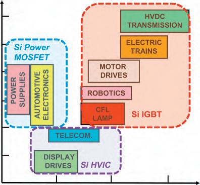
1.2Siliconpowerdeviceapplications Powerdevicesareusedinallsectorsoftheeconomywithsystemsthatoperateover abroadspectrumofpowerlevelsandfrequencies.Theapplicationsforpower devicesareshownasafunctionofoperatingfrequencyin
Fig.1.1.Highvoltage directcurrent(HVDC)powerdistributionandlocomotivedrivesthatrequirethe
controlofmegawattsofpoweroperateatrelativelylowfrequencies.Thepowerratingsdecreaseforthedeviceswhentheoperatingfrequencyincreaseswithtypical microwavedeviceshandlingabout100W.Alloftheseapplicationsareservedby silicondevicestoday.PowerMOSFETsarepreferredforthehighfrequencyapplicationsoperatingfromlowpowersourcevoltages.Theseapplicationsinclude powersuppliesforcomputersandlaptops,powermanagementinsmartphones,and automotiveelectronics.Untilrecently,thyristorsweretheonlydevicesavailable withsufficientvoltageandcurrentratingsfavoredfortheHVDCpowerdistribution applications.TheratingsofIGBTshavenowgrowntolevelswheretheyarenow preferredoverthyristorsforvoltagesourceconvertersandflexiblealternatingcurrenttransmission(FACTs)designs.Themediumfrequencyandpowerapplications suchaselectrictrains,hybrid-electriccars,homeappliances,compactfluorescent lamps,medicalequipment,andindustrialmotordrivesalsoutilizetheIGBT. Siliconpowerdevicescanalsobeclassifiedbasedontheircurrentand voltage-handlingrequirementsasshownin Fig.1.2 .Thyristorsareavailablethat canindividuallyhandleover6000Vand2000Aenablingthecontrolofover
Figure1.1 Applicationsforpowerdevicesoverabroadrangeoffrequencies.
Applicationsforsiliconpowerdevicesusingsystemvoltageandcurrentratings.
10MWofpowerbyasinglemonolithicdevice.Thesedevicesaresuitablefor theHVDCpowertransmissionapplications.Duringlast10years,siliconIGBT moduleshavebeendevelopedwithblockingvoltagesofupto6500Vandcurrenthandlingcapabilityabove1000A.ThishasallowedthesiliconIGBTto replacethyristorsinHVDC.ThesiliconIGBTistheoptimumsolutionfora broadrangeofsystemsthatrequireoperatingvoltagesbetween300Vand 3000Vwithsignificantcurre nthandlingcapability.These applicationsspanall sectorsoftheeconomyincludingconsumer,industrial,transportation,lighting, medical,defense,andrenewableenergygeneration [1] .Itisfeasibletointegrate multiplesilicondevicesonasinglemonol ithicchipwhenthecurrentrequirementsfallbelow1Atoprovidegreaterfunctionalityforsystemssuchastelecommunicationsanddisplaydrives.However,whenthecurrentexceedsafew amperes,itismorecosteffectivetousediscretepowerMOSFETswithappropriatecontrolICstoserveapplicationssuchasautomotiveelectronicsand switchmodepowersupplies.
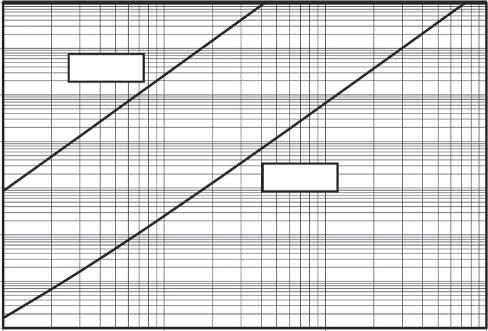
1.3Siliconcarbideidealspecificon-resistance Theidealspecificon-resistanceforthedriftregioninaverticalunipolarpower devicesisgivenby [2]:
Figure1.2
Figure1.3 Idealspecificon-resistanceforsiliconcarbidepowerdevices.
where εS isthedielectricconstantofthesemiconductor, μn istheelectronmobility, and EC isthecriticalelectricfieldforbreakdowninthesemiconductor.ThedenominatoriscalledBaliga’sfigure-of-merit(BFOM) [3,4]:
Itisameasureofthepower-handlingcapability(W/cm2)ofapowerdevice. Unipolarsiliconcarbidepowerdeviceshavelowon-statevoltagedropduetoits largeBFOM.Thisismainlyduetotheapproximatelytenfoldincreaseincritical electricfieldforbreakdownforSiCcomparedwithsilicon.
Theidealspecificon-resistanceforthedriftregionin4H-SiCdevicesiscomparedwiththatforsiliconin Fig.1.3 forbreakdownvoltagesfrom100to 100,000V.Asignificantreductioninthespecificon-resistanceofdriftregionsis predictedbyreplacingsiliconwith4H-SiC.Theratioofthespecificon-resistance forsilicontothatfor4H-SiCincreasesfrom527atabreakdownvoltageof100V to1280forbreakdownvoltagesabove40,000V.
1.4Siliconcarbidepowerrectifiers SiliconbipolarpowerP i Ndiodesoperatewiththeinjectionofminoritycarriers duringon-statecurrentflow [2].Thesecarriersmustberemovedwhenswitching thedevicefromtheon-statetotheoff-state.Thisisaccomplishedbythereverse recoveryprocessthatproducesalargereversecurrentduringturnoff.Thiscurrent producessignificantpowerlossesinthediodeandtheswitchesinthecircuits.
SCHOTTKY CONTACT METAL (ANODE) OHMIC CONTACT METAL (CATHODE) Itisthereforepreferabletoutilizeunipolarcurrentconductioninapowerdiode. ThecommonlyusedunipolarpowerdiodestructureistheSchottkyrectifierthatutilizesametal-semiconductorbarriertoproducecurrentrectification.ThehighvoltageSchottkyrectifierstructurecontainsadriftregion,asshowin Fig.1.4,whichis designedtosupportthereverseblockingvoltage.Theresistanceofthedriftregion increasesrapidlywithincreasingblockingvoltagecapability.SiliconSchottkyrectifiersarecommerciallyavailablewithblockingvoltagesofupto150V.Beyondthis value,theon-statevoltagedropofsiliconSchottkyrectifiersbecomestoolargefor practicalapplications.SiliconP i Nrectifiersarefavoredfordesignswithlarger breakdownvoltagesduetotheirloweron-statevoltagedropdespitetheirslower switchingproperties.
SiliconcarbideSchottkyrectifiershavemuchlowerdriftregionresistance enablingdesignofveryhighvoltagedeviceswithlowon-statevoltagedrop.These devicesareexcellentreplacementsforsiliconP i Nrectifiersusedasfly-backor free-wheelingdiodeswithIGBTsininverters.However,amajorproblemobserved inSiCSchottkyrectifiersisthelargeincreaseinthereverseleakagecurrentwith increasingreversebiasvoltage.Anincreaseinreverseleakagecurrentbyfive ordersofmagnitudeoccursduetoSchottkybarrierloweringandtunneling.Thisis aseriousproblemforhightemperatureoperationandstabilityfortheserectifiers.
TherapidincreaseinleakagecurrentforSchottkyrectifierswithincreasing reversebiasvoltagecanbemitigatedbyusingthejunction-barriercontrolled
Figure1.4 ThebasicSchottkyrectifierstructure.
Figure1.5 ThesiliconJBSrectifierstructure.
Schottky(JBS)structure [5,6] shownin Fig.1.5.ThisstructurecontainsP1 regions surroundingtheSchottkycontacts.Adepletionregionextendsfromthejunction andformsapotentialbarrierundertheSchottkycontact.ThissuppressestheelectricfieldattheSchottkycontact.ThelowerelectricfieldattheSchottkycontact reducestheSchottkybarrierloweringandtunnelingatthecontact [7]
1.5SiliconpowerMOSFETs ThecommerciallyavailablesiliconpowerMOSFEThasbeenwidelyusedforlower powerapplicationswherethesupplyvoltagesarebelow200V.Thecommercially availablesiliconpowerMOSFETproductsarebaseduponthestructuresshownin Fig.1.6.IntheD-MOSFETstructure,theP-baseregionandtheN1 sourceregions areself-alignedtotheedgeofthepolysilicongateelectrodebyusingionimplantationofboronandphosphoruswiththeirrespectivedrive-inthermalcycles. TheN-typechannelisdefinedbythedifferenceinthelateralextensionofthejunctionsunderthegateelectrode.Thedevicesupportspositivevoltageappliedtothe drainacrosstheP-base/N-driftregionjunction.Thevoltageblockingcapabilityis determinedbythedopingandthicknessofthedriftregion.Althoughlowvoltage ( , 100V)siliconpowerMOSFEThavelowon-resistances,thedriftregionresistanceincreasesrapidlywithincreasingblockingvoltagelimitingtheperformance ofsiliconpowerMOSFETstobelow200V.ThesiliconU-MOSFETstructurehas agatestructureembeddedwithinatrenchetchedintothesiliconsurface.The N-typechannelisformedontheside-wallofthetrenchatthesurfaceoftheP-base region.Thechannellengthisdeterminedbythedifferenceinverticalextensionof
theP-baseandN1 sourceregionsascontrolledbytheion-implantenergiesand drivetimesforthedopants.ThesiliconU-MOSFETstructurewasdevelopedto reducetheon-stateresistancebyeliminationoftheJFETcomponentwithinthe D-MOSFETstructure [2].
Thechargecouplingconceptwasanimportantinnovationforsiliconpower MOSFETs.Italterstheelectricfielddistributioninthedriftregionandallowssupportinghighvoltageswithlargedopingconcentrationsinthedriftregion [8].The firstchargecoupledverticalsiliconpowerMOSFETwastheGD-MOSFETstructureshownin Fig.1.7 ontheleft-handside [9,10].Thedevicecontainsadeep trenchregionwithasourceconnectedelectrode.Auniformelectricfieldcanbe generatedinthedriftregionbyusingagradeddopingprofileinthedriftregion withhighdopingconcentrations [11].Breakdownvoltageswellabovetheparallelplanebreakdownvoltagecanbeachievedusingthisidea.Thespecificonresistanceofthesedeviceshasbeenshowntobewellbelow(5to25times)that fortheconventionalsilicondevicesforblockingvoltagesrangingfrom50to 1000V [6].Manycompanieshavereleasedproductsusingthisapproach.
Analternatecharge-coupledsiliconpowerMOSFETistheCOOLMOSstructure shownin Fig.1.7 ontheright-handside.Here,thechargecouplingisaccomplished acrosstheverticalP NjunctionformedbetweencolumnsofPandNdriftregions [12].Manystudieshavebeenperformedtooptimizethisdevicestructureforblockingvoltagesof500 1000V [6].IthasbeendemonstratedthattheCOOLMOS structurehasabout3to10timeslowerspecificon-resistancethantheconventional
Figure1.6 ThesiliconpowerMOSFETstructures.
Thesiliconcharge-coupledpowerMOSFETstructures.
siliconpowerMOSFETsatabreakdownvoltageof600V.Manycompanieshave commercializedthisdevicestructureundervariousnames.
AnyproposedGaNorSiCpowerswitchtechnologymustcompetewithnotonly theconventionalsiliconpowerMOSFETstructuresbutalsothenewchargecoupled siliconpowerMOSFETs.Thechargecoupledsilicondevicesoffermuchbetterperformancebutrequireamoreexpensivefabricationprocess.Thisdifferencemust alsobetakenintoaccount.
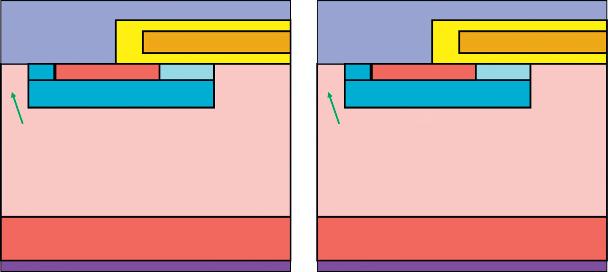
1.6SiliconcarbidepowerMOSFETs ThesiliconD-MOSFETstructurecannotbereplicatedinsiliconcarbideforseveral reasons.First,thedopantsinsiliconcarbidedonotdiffuseevenatveryhightemperatures.Consequently,thechannelinsiliconcarbideplanarpowerMOSFETsis createdbystaggeringtheP-baseandN1 sourceionimplants [13].Thishasbeen calledthedouble-implantedorDI-MOSFETstructure [14].Second,alargeamount ofdepletionoccursintheP-baseregionofsiliconcarbidedevicesduetothelarge electricfieldattheblockingjunction [15].Thisleadstoverylargechannellength resultinginpooron-resistanceofdevices.Thisproblemcanbesolvedbyusingthe shieldedSiCplanarpowerMOSFETstructures [16] shownin Fig.1.8 witheither aninversionlayeroranaccumulationlayerchannel.AdeepP1 shieldingregion hasbeenincorporatedintothestructurestopreventthedepletionofthebase regions.Inthecaseofthestructurewiththeinversionlayerchannel,theP1 shieldingregionextendsunderboththeN1 sourceregionaswellasundertheP-base region.Inthecaseofthestructurewiththeaccumulationlayerchannel,theP1 shieldingregionextendsundertheN1 sourceregionandtheN-baseregionlocated underthegate.ThisN-baseregioncanbeformedusinganuncompensatedportion
Figure1.7
Figure1.8 TheshieldedSiCpowerMOSFETstructures.
oftheN-typedriftregionoritcanbecreatedbyaddingN-typedopantsnearthe uppersurfacewithionimplantationorepitaxialgrowthtoindependentlycontrolits thicknessanddopingconcentration.
Anotherimportantproblemforsilic oncarbidepowerMOSFETsisthelarge electricfieldgeneratedinthegateoxideduetothelargeelectricfieldinthe semiconductorwhenblockinghighvoltages.Thisproblemcanbeovercomeby usingtheshieldedstructuresshownin Fig.1.8 .ThegapbetweentheP 1 shieldingregionsisoptimizedtoobtainalowspecificon-resistancewhilesimultaneouslyshieldingthegateoxideinterfacefromthehighelectricfieldinthedrift region.
Ithasbeendemonstratedthatsignificantlylargermobilityforelectronsis observedinthechannelforaccumulation-modeSiCpowerMOSFETswhencomparedwithinversion-modeSiCpowerMOSFETs [17].Thisallowsreducingthe specificon-resistanceofSiCpowerMOSFETswithblockingvoltagesbelow3kV. Fordeviceswithlargerblockingvoltages,thedriftregionresistancebecomesdominant [18].Atpresent,mostoftheSiCpowerMOSFETcommercializationeffortis focusedondeviceswithblockingvoltagesof1.2and1.7kV.
1.7SiliconcarbidepowerjunctionbarrierSchottkyfield effecttransistors(JBSFETs) Mostapplicationsforpowerdevicesrequirecurrentflowinnotonlythefirst quadrantbutalsointhethirdquadrant.Onecommonsuchapplicationisthe
H-bridgecircuitusedformotorcontrol.Thepresenceofthebodydiodeinthe powerMOSFETstructureprovidesaconvenientpathforcurrentflowinthe thirdquadrant.Alternately,thegatecanbeturnedonevenwhenthedrainvoltagehasanegativepotentialallo wingcurrentflowviathechannel. Unfortunately,theperfectsynchroni zationofthegatesignalwiththeswitching ofthedrainvoltageintothethirdquadrantisnotpossibleproducingcurrent flowviathebodydiode.ForSiCpowerMO SFETs,theon-statevoltagedropfor thebodydiodeexceeds4Vproducinghigh conductionlosses.Inaddition,the bodydiodeconductionintroducesminoritycarrierinjectionandstoredchargein thedriftlayer.Theremovalofthestoredchargeisaccompaniedbyareverse recoverycurrentthatproducesenhancedturn-onswitchinglossesinthe MOSFETs.Ithasalsobeenfoundthat powerMOSFETcharacteristicscanbe degradedwhenthebodydiodeisturned-onduetothegenerationofstacking faultsatbasalplanedislocations.
TheaboveproblemshavebeenovercomebycreatingtheSiCjunctionbarrier controlledSchottkyfieldeffecttransistor(JBSFET)structurewhereaJBSdiode isintegratedintothepowerMOSFETstructure [19,20] asillustratedin Fig.1.9 IthasbeendemonstratedthattheJBSdiodeinsidetheJBSFETcanbefabricated usingasinglemetaltomaketheohmiccontactstotheN 1 sourceregionandthe P-baseregionwhileproducingaSchottkycontacttotheN-drainregion.TheJBS diodehasavoltagedropofonly2Vwhenconductingcurrentinthethirdquadrantwhichpreventsturn-onoftheMOSFETP Njunctionbodydiode.
Figure1.9 TheSiCpowerJBSFETstructure.
1.8SiliconcarbidepowerMOSFETswithimprovedhigh frequencyperformance InordertomaximizethebenefitsofreplacingthesiliconIGBTwithSiCpower MOSFETs,itisnecessarytoincreasethecircuitoperatingfrequencytoreduce thesizeandcostofpassiveelements.SiCpowerMOSFETsmustbeoptimizedto reducetheirswitchinglosses.Thiscanbeachievedbyreducingthereversetransfer capacitance(CGD)withinnovationsinthegatestructure.Twodevicestructuresthat produceasignificantlyimproved(smaller)high-frequencyfigures-of-merit (HFFOM),definedby[Ron CGD]and[Ron QGD],areshownin Fig.1.10
Thesplit-gate(SG)-MOSFETstructurehasapolysilicongatewithan openinginthemiddleofthegateelectrode whereitoverlapsthedriftregion.This structurecanbefabricatedusingthesameprocessusedtomaketheconventional SiCplanar-gatepowerMOSFET.ThemeasuredHFFOM[Ron CGD ]forthe SG-MOSFEThasbeenfoundtobe1.3times smallerthanfortheconventional MOSFETwhileitsHFFOM[R on QGD]is2.4timessmallerthanfortheconventionalMOSFET [21]
Thebuffered-gate(BG)-MOSFETstructurehasapolysilicongatewithanopeninginthemiddleofthegateelectrodewhereitoverlapsthedriftregion.Inaddition,theP1 shieldingregionisextendedbeyondtheedgeofthegateelectrodeto completelyscreenitfromthedrain.TopreventcompletedepletionoftheN-type regionabovetheP1 shieldingregion,itisnecessarytoaddasecondjunctionfield effecttransistor(JFET)2regionwithhigherdopingconcentrationthanintheJFET 1region.ThemeasuredHFFOM[Ron CGD]fortheBG-MOSFEThasbeenfound
tobe3.6timessmallerthanfortheconventionalMOSFETwhileitsHFFOM [Ron QGD]is4.0timessmallerthanfortheconventionalMOSFET [22].
1.9Siliconcarbidebidirectionalfieldeffecttransistor Matrixconvertersrequirepowerdevicesthatcanblockhighvoltageinthefirstand thirdquadrantsandcarrygatecontrolledcurrentinbothquadrants [23].Thedevelopmentandcommercializationofthesetypesofconvertershasbeenhinderedby thelackofavailabilityofacost-effectivebidirectionalswitchwithlowon-state voltagedropandswitchinglosses.Manyapproachestocreatingabidirectional switchhavebeenproposedusingsiliconIGBTsandSiCpowerMOSFETs.They requiremultipleindependentlypackageddeviceswithahighneton-statevoltage drop.
TheSiCbidirectionalfieldeffecttransistor(BiDFET)wasproposedtoaddress thisapplication [24].ItconsistsoftwoSiCJBSFETsconnectedinseriesasshown in Fig.1.11.Thesedevicescanalsobemonolithicallyintegratedbybuildingthem adjacenttoeachotheronthesameSiCwafer.TerminalT1servesasthereference terminaloftheBiDFETwithhighACvoltagesappliedtoterminalT2.Bothgates G1andG2areusedtocontroltheoperationofthedeviceinthefirstandthird quadrant.Itisworthemphasizingthat,unlikeconventionalpowerMOSFETs,no externalelectricalconnectionisperformedtotheN1 substrate(drain)intheproposedBiDFET.
HighblockingvoltagecapabilityinthefirstquadrantisachievedintheBiDFET withzerobiasappliedtogateG1withrespecttoterminalT1.Underthese
conditions,thebodydiodeofpowerJBSFET2isforwardbiasedandthehighvoltageissupportedacrosspowerJBSFET-1anditsedgetermination.Highblocking voltagecapabilityinthethirdquadrantisachievedwithzerobiasappliedtogate G2withrespecttoterminalT2.Undertheseconditions,thebodydiodeofpower JBSFET1isforwardbiasedandthehighvoltageissupportedacrosspower JBSFET-2anditsedgetermination.
CurrentconductioninthefirstquadrantisachievedintheBiDFETbytheapplicationofapositivegatedrivevoltagetobothgatesG1andG2withreferenceto thecorrespondingterminalsT1andT2.Thisturns-onthechannelforbothSiC powerJBSFETs.Theon-resistanceoftheBiDFETisthenthesumoftheonresistanceofbothSiCpowerJBSFETs1and2.Itcanbereducedasdesiredby scalingtheareaofbothpowerJBSFETstoachievealowon-statevoltagedrop.
Gatevoltage-controlledcurrentsaturationwithexcellentoutputcharacteristicsis achievedintheBiDFETaspreviouslydemonstratedforSiCpowerMOSFETs.The BiDFETalsohasfastswitchingcapabilityaspreviouslydemonstratedforSiC powerMOSFETs.Thesefeaturesmakeitwellsuitedformatrixconvertersoperatingathighfrequenciestoachievehighpowerdensity.
Oneoftheproblemsthatcanbeencounteredinbidirectionalswitchesusedin matrixconvertersoccursduringthedead-timeorcommutation-time.Thiscanlead tocurrentconductionviathebodydiodeintheMOSFETs.Ithasbeendocumented thatcurrentflowviathebodydiodeofSiCpowerMOSFETscanleadtobipolar degradationofthedevices.ThisproblemiscircumventedintheBiDFETbyimplementingitusingSiCJBSFETs.Inthiscase,thecurrentflowoccursviatheintegratedJBSdiodeswithintheJBSFETstructurepreventingcurrentfollowviathe P Nbodydiodetocompletelysuppressthebipolardegradationphenomenon.
TheBiDFEThasbeenexperimentallydemonstratedwith1.2kVratedJBSFETs [25].Thedeviceswereshowntoexhibitgatevoltage-controlledoutputcharacteristicsinthefirstandthirdquadrantwithblockingvoltagesofupto1650V.Theonresistanceofthedevicesinbothquadrantsisthesumoftheresistanceofeachof theJBSFETswiththeon-stategatebiasof20V.Theon-statecharacteristicsexhibit akneeofabout1Vifthegatevoltageisnotappliedtothedevicewiththeforward biasedJBSdiode.TheBiDFETrequiresonlyasinglepackageincontrasttopreviousbidirectionalswitchesthatneed4 6separatelypackageddevices.Itson-state voltagedropcanbereducedtoonly0.5Vbyscalingtheon-resistanceofthe JBSFETscomparedwithmorethan1.25Vforthepriordevices.
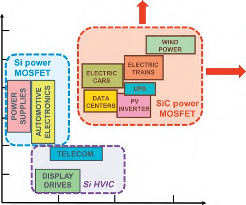
1.10Siliconcarbidepowerdeviceapplications Inprinciple,siliconcarbidepowerMOSFETsareexcellentcandidatestoreplace siliconIGBTsinalltheirapplicationsbecauseoftheirlowon-resistanceand reducedswitchinglosses.However,thecostoftheSiCpowerMOSFETsissubstantiallylargerthanthatofthesiliconIGBT.Asaconsequence,SiCpower MOSFETshavebeensuccessfullyusedinselectedapplicationsasshownin
ApplicationsforSiCpowerMOSFETstructures.
Fig.1.12.Oneoftheseapplicationsisinvertersforsolarpowergeneration.The replacementofsiliconIGBTswithSiCpowerMOSFETshasbeenshownto increasetheefficiencyby1% 2%.Thismodestgaininenergygenerationoffsets thelargerinitialcostoftheSiCdevices.
AnotherpromisingapplicationforSiCpowerMOSFETsisininvertersforelectricandhybrid-electricvehicles.Theimprovedinverterefficiencyallowsextending therangeofthevehicles.Inaddition,theSiCinverterscanbeoperatedathigher frequenciesthanthosebasedonsiliconIGBTs.Thisallowsreductionofpassive componentsizeandweight,animportantbenefitforinelectricvehicles.
AsthecostofSiCpowerMOSFETisreducedinthefuture,itisanticipatedthat theirapplicationswillexpandasindicatedbythearrowsin Fig.1.12.ThepenetrationofSiCpowerMOSFETsintoapplicationsservedbytheSiIGBTwillbeacceleratedbymakingproductswithsuperiorHF-FOMs,suchastheSG-MOSFETand BG-MOSFET.
1.11Galliumnitridepowerdevices Thecommercializationofgallium nitridedeviceswasacceleratedbythesuccessful growthofhighqualitygalliumnitridelayersonsiliconsubstratesbyusingatransitionlayerasillustratedin Fig.1.13 toamelioratethelatticemismatchbetweenthe materials.ThecostofthewafersisgreatlyreducedincomparisonwithSiCorGaN
Figure1.12
SOURCE DRAIN substratesbytheuseoflargediametersiliconsubstrates.Athinaluminum gallium nitridelayerisformedontopofthegalliumnitridelayertoproducethetwodimensionalelectrongasinthegalliumnitride.Theelectronsinthetwo-dimensional electrongashaveahighmobility(B2000cm2/Vs)andcharge(B1013 cm 2).This createsahighconductivitycurrentpaththroughtheGaNdriftregionwithlowspecificon-resistancedespitethelateraldevicestructure.Thisallowscreatinglateral deviceswithhigh-blockingvoltagesandlow-specificon-resistance.
GaNHEMTstructureshavebeendemonstratedwithveryhighblockingvoltages.However,commercialdeviceshaveblockingvoltagesintherangeof 600 900V.TheinterdigitatedcellstructureforthelateralGaNHEMTdeviceis difficulttoscaletohighercurrentlevels.Thisisrestrictedthecurrentratings between50Aand100A.Furthermore,ithasbeendifficulttoachievean enhancement-modelateralGaNHEMTdevice.Unfortunately,normally-ondevices areunacceptableforpowerelectronicsapplications.Normally-offGaNdevices havebeenrealizedbyusingtheBaliga-Pairorcascodeconfiguration.IntheBaligaPair [26],anormally-onsiliconcarbidehighvoltageJFET/MESFETdeviceora GaNHEMTdeviceisusedtogetherwithalowvoltagesiliconMOSFETtocreatea configurationwiththedesiredfeaturesforahigh-qualitypowerswitch.Thebasic ideaisillustratedin Fig.1.14.ItconsistsofahighvoltagesiliconcarbideJFETor MESFETstructurewithitssourceelectrodeconnectedtothedrainelectrodeofa lowvoltagesiliconpowerMOSFET.Animportantfeatureofconfigurationisthat thegateofthesiliconcarbidedeviceisconnectedtothesourceofthesiliconpower MOSFETwhichservesasthegroundorreferenceterminalincircuits.Gatesignals areexclusivelyappliedtothegateofthesiliconpowerMOSFET.Thedrainofthe siliconcarbidedeviceisconnectedtotheloadinpowercircuitsaswouldbedone withthedrainofsiliconpowerMOSFETs.TheBaliga-PairconfigurationisathreeterminalpowerswitchwithanMOS-inputinterfaceprovidedbythesiliconpower
SILICON SUBSTRATE
Figure1.13 TheGaNHEMTstructureformedonasiliconsubstrate.