Wearable Bioelectronics
Edited By Onur Parlak
Postdoctoral Research Fellow, Materials Science and Engineering, Stanford University, Stanford, CA, United States Alberto Salleo
Associate Professor of Materials Science, Stanford University, Stanford, CA, United States Anthony Turner
Emeritus Professor of Biotechnology, SATM, Cranfield University, Cranfield, Bedfordshire, United Kingdom
Elsevier
Radarweg 29, PO Box 211, 1000 AE Amsterdam, Netherlands
The Boulevard, Langford Lane, Kidlington, Oxford OX5 1GB, United Kingdom
50 Hampshire Street, 5th Floor, Cambridge, MA 02139, United States
© 2020 Elsevier Ltd. All rights reserved.
No part of this publication may be reproduced or transmitted in any form or by any means, electronic or mechanical, including photocopying, recording, or any information storage and retrieval system, without permission in writing from the publisher. Details on how to seek permission, further information about the Publisher’s permissions policies and our arrangements with organizations such as the Copyright Clearance Center and the Copyright Licensing Agency, can be found at our website: www.elsevier.com/permissions
This book and the individual contributions contained in it are protected under copyright by the Publisher (other than as may be noted herein).
Notices
Knowledge and best practice in this field are constantly changing. As new research and experience broaden our understanding, changes in research methods, professional practices, or medical treatment may become necessary.
Practitioners and researchers must always rely on their own experience and knowledge in evaluating and using any information, methods, compounds, or experiments described herein. In using such information or methods they should be mindful of their own safety and the safety of others, including parties for whom they have a professional responsibility.
To the fullest extent of the law, neither the Publisher nor the authors, contributors, or editors, assume any liability for any injury and/or damage to persons or property as a matter of products liability, negligence or otherwise, or from any use or operation of any methods, products, instructions, or ideas contained in the material herein.
Library of Congress Cataloging-in-Publication Data
A catalog record for this book is available from the Library of Congress
British Library Cataloguing-in-Publication Data
A catalogue record for this book is available from the British Library
ISBN: 978-0-08-102407-2
For information on all Elsevier publications visit our website at https://www.elsevier.com/books-and-journals
Publisher: Matthew Deans
Acquisition Editor: Kayla Dos Santos
Editorial Project Manager: Joshua Mearns
Production Project Manager: Maria Bernard
Cover Designer: Christian J. Bilbow
Typeset by SPi Global, India
Contributors
Yuanyuan Bai Suzhou Institute of Nano-tech and Nano-bionics, Chinese Academy of Sciences, Beijing, China
Lourdes Basabe-Desmonts BIOMICs Research Group, Lascaray Ikergunea, Research Center, University of the Basque Country, Vitoria-Gasteiz; Ikerbasque, Basque Foundation for Science, Bilbao, Spain
Fernando Benito-Lopez Analytical Microsystems & Materials for Lab-on-a-Chip (AMMa-LOAC) Group, Microfluidics Cluster UPV/EHU, Analytical Chemistry Department, University of the Basque Country UPV/EHU, Vitoria-Gasteiz, Spain
Vincenzo F. Curto Electrical Engineering Division, Department of Engineering, University of Cambridge, Cambridge, United Kingdom
Sergio Curto Radiation Oncology, Erasmus MC Cancer Institute, Rotterdam, The Netherlands
Ravinder Dahiya School of Engineering, University of Glasgow, Glasgow, United Kingdom
Sam Emaminejad Interconnected and Integrated Bioelectronics Lab, Department of Electrical and Computer Engineering, University of California, Los Angeles, CA, United States
Edwin W.H. Jager Division of Sensor and Actuator Systems, Department of Physics, Chemistry and Biology (IFM), Linköping University, Linköping, Sweden
Jose G. Martinez Division of Sensor and Actuator Systems, Department of Physics, Chemistry and Biology (IFM), Linköping University, Linköping, Sweden
Sina Moshfeghi Interconnected and Integrated Bioelectronics Lab, Department of Electrical and Computer Engineering, University of California, Los Angeles, CA, United States
William Navaraj School of Engineering, University of Glasgow, Glasgow, United Kingdom
Edilberto Ojeda Analytical Microsystems & Materials for Lab-on-a-Chip (AMMa-LOAC) Group, Microfluidics Cluster UPV/EHU, Analytical Chemistry Department, University of the Basque Country UPV/EHU; BIOMICs Research Group, Lascaray Ikergunea, Research Center, University of the Basque Country, Vitoria-Gasteiz, Spain
Onur Parlak Department of Materials Science and Engineering, Stanford University, Stanford, CA, United States
Nils-Krister Persson Smart Textiles, Swedish School of Textiles (THS), University of Borås, Borås, Sweden
Sanaz Pilehvar Interconnected and Integrated Bioelectronics Lab, Department of Electrical and Computer Engineering, University of California, Los Angeles, CA, United States
Punit Prakash Electrical and Computer Engineering, Kansas State University, Manhattan, KS, United States
Contributors
Kamyar Salahi Interconnected and Integrated Bioelectronics Lab, Department of Electrical and Computer Engineering, University of California, Los Angeles, CA, United States
Alberto Salleo Department of Materials Science and Engineering, Stanford University, Stanford, CA, United States
Alina Sekretaryova Department of Chemistry, Uppsala University, Uppsala, Sweden
Clara Smith School of Engineering, University of Glasgow, Glasgow, United Kingdom
Phoenix Stout Interconnected and Integrated Bioelectronics Lab, Department of Electrical and Computer Engineering, University of California, Los Angeles, CA, United States
Minyoung Suh Textile and Apparel, Technology and Management, North Carolina State University, Raleigh, NC, United States
Gerard van Rhoon Radiation Oncology, Erasmus MC Cancer Institute, Rotterdam, The Netherlands
Shuqi Wang Suzhou Institute of Nano-tech and Nano-bionics, Chinese Academy of Sciences, Beijing, China
Bo Wang Interconnected and Integrated Bioelectronics Lab, Department of Electrical and Computer Engineering, University of California, Los Angeles, CA, United States
Andrew Wilhelm Interconnected and Integrated Bioelectronics Lab, Department of Electrical and Computer Engineering, University of California, Los Angeles, CA, United States
Aaron Wilhelm Interconnected and Integrated Bioelectronics Lab, Department of Electrical and Computer Engineering, University of California, Los Angeles, CA, United States
Ting Zhang Suzhou Institute of Nano-tech and Nano-bionics, Chinese Academy of Sciences, Beijing, China
Yong Zhong Division of Sensor and Actuator Systems, Department of Physics, Chemistry and Biology (IFM), Linköping University, Linköping, Sweden
Preface
We are delighted to introduce the very first book on Wearable Bioelectronics, to serve the global community with topical critical and tutorial reviews covering aspects of bioelectronic technology and engineering.
Wearable technologies are one of the most important and recent breakthroughs in the bioelectronics field and have attracted considerable attention because of their potential to change classical and established approaches in medicine and biotechnology. Wearable bioelectronics offer huge promise due to their ease of miniaturization, the possibility of rapid and in situ analysis, and the potential for low-cost fabrication. With more innovation and further attention to overcome technical hurdles, novel approaches and methodologies are expected to open up new and exciting avenues for the maintenance of well-being and the delivery of personalized health care. However, achieving these paradigm shifts requires significant progress and research into new materials, interfaces, circuit designs, power sources, and data processing, together with new business models. With this book, we aim to survey recent trends in wearable bioelectronics and their implications for health-care applications. In Chapter 1, Ting Zhang et al. provide an overview of the importance of materials and systems for wearable designs, introducing the reader to different materials and how they influence device performance. The following chapters (Chapter 2 by Emaminejad et al. and Chapter 3 by Parlak et al.) piece together different types of wearable sensors, including physical and (bio)chemical sensors, to highlight and discuss challenges, early breakthroughs, and key developments in point-of-care diagnostics. These chapters also draw attention to sample handling strategies for various wearable sensor systems. In Chapter 4, Alina Sekretaryova stresses the importance of powering strategies for wearable bioelectronic devices and outlines various different approaches. Moving toward applying these principles to develop innovative devices for the bioelectronic world, Dahiya et al. review the fascinating field of e-skin for health care in Chapter 5, and Suh et al. introduce the new concept of wearable devices for thermotherapies in Chapter 6. Finally, Jager et al. describe textile-based artificial muscles in Chapter 7, where electronic methods are employed to yield functional wearable devices. Each of these chapters concludes with a discussion of key examples in their respective areas and their implications in the field of wearable bioelectronics.
Preface
We hope you enjoy this book as much as we have enjoyed putting it together. It remains for us to thank all the contributing authors for their enthusiasm and patience and the editorial publishing team of Elsevier for all diligent work, and particularly Joshua Mearns and Kayla Dos Santos for enabling the publication of this book.
Onur Parlak, Anthony P.F. Turner, Alberto Salleo
CHAPTER 1
Materials, systems, and devices for wearable bioelectronics
Shuqi Wang1, Yuanyuan Bai1, Ting Zhang*
Suzhou Institute of Nano-tech and Nano-bionics, Chinese Academy of Sciences, Beijing, China
Chapter Outline
1.1 Introduction 1
1.2 Materials and structural design for flexible/stretchable sensors 2
1.2.1 Flexible/stretchable substrate 3
1.2.2 Functional/active materials 5
1.2.3 Stretchable electrodes 12
1.2.4 Structural approaches for flexibility/stretchability 14
1.3 Flexible/stretchable sensor devices for wearable bioelectronics 18
1.3.1 Pressure/strain sensors 19
1.3.2 Temperature sensors 24
1.3.3 (Bio)chemical sensors 29
1.4 Conclusions and perspectives 33
References 34
Further reading 44
1.1 Introduction
Wearable bioelectronics, research on sophisticated state-of-the-art wearable devices which enable real-time monitoring of individuals’ physiological parameters, has attracted much interest from researchers and clinicians in the recent years [1–5]. Researchers and clinicians believe that wearable devices could not only lead to significant improvements in personal health monitoring, to track one’s metabolic status in real time for timely and effective diagnosis and treatment of diseases, but also bring tremendous benefits by building more advanced health-care systems. By using sophisticated wearables, a wide range of physical and (bio) chemical signals such as heart rate, blood pressure, respiration, body motion, body temperature, electrophysiological signs [e.g., electrocardiogram (ECG) and electroencephalogram (EEG)],
* Corresponding author.
1 These authors contributed equally.
Wearable Bioelectronics. https://doi.org/10.1016/B978-0-08-102407-2.00002-3
and biofluids’ (e.g., sweat, tears, saliva) components (e.g., electrolytes and metabolites) are available for real-time monitoring with clinical or health-care importance [6–9]. This makes it possible for portable and systematic home monitoring, which holds the promise to be used for remote medicine practices by connecting with the Internet of Things [10].
Wearable bioelectronic devices are basically represented by several components including the sensor module, processing module, communication module, and powering module, which are required to be mounted on soft skin, curved surfaces, or moving joints. Therefore, flexibility and stretchability are essential for their intimate and comfortable wearability. Thanks to the progress in this field, dedicated operating system, low-power wireless technologies, miniaturized and flexible sensor units that meet the requirements for wearable bioelectronics are available now. In the recent years, several groups have bridged the gap between those technologies and developed fully integrated wearable bioelectronic device prototypes for on-body physiological signal analysis [11–13]. However, the development of wearable sensors and systems is still in its infancy, researchers have been engaged in developing the technologies of sensing, computing, and processing to enable wearable bioelectronics to revolutionize the way medicine and health care are practiced.
This chapter focuses on the essential component of the flexible/stretchable sensor module in wearable bioelectronic device. Traditional sensors consisted of transducer (e.g., conductive electrode, semiconductor, piezoelectric, and piezoresistive materials) and active materials (e.g., sensitive inorganic materials, enzyme, ion-selective membrane) are rigid and planar (the hybrid materials of sensors have high Young’s modulus about 100 GPa), which are mechanically incompatible with soft and curvilinear human body (human tissues have low Young’s modulus from < 10 kPa of brain to hundreds kPa of skin), resulting in unreliable results due to the mismatch with skin [3]. Advances have been made in the recent years to develop flexible and stretchable sensors that can be attached intimately to the clothing or directly mounted on the skin for stable and accurate measurements. The following part of this chapter will address the latest strategies of using high-quality materials, novel processing approaches, and special configuration designs for fabrication of flexible/stretchable sensors. Moreover, lightweight wearable bioelectronic devices which can be conformably worn on human body for not only physical activities and vital signs monitoring (e.g., heart rate, respiration, body motion, body temperature), but also for biochemical signal analysis at molecular level (e.g., pH, electrolytes, metabolites) are demonstrated. Challenges and future prospects of flexible sensors are also discussed.
1.2 Materials and structural design for flexible/stretchable sensors
Conformal contact between flexible/stretchable sensor devices and human body can be achieved by matching the mechanical properties of the devices with those of the human tissues. The mounted sensor devices should maintain stable electrical properties under certain level of deformation (e.g., strain tolerance of more than 80% on knuckle, 50% on knee joint, and 30% on arm angle) [4, 14]. Generally, mechanical flexibility and stretchability
Materials, systems, and devices for wearable bioelectronics 3 can be achieved by using intrinsically flexible/stretchable materials, or by special structural design. Various intrinsically flexible/stretchable materials such as elastomeric polymers and nanocomposites have been used as substrates, active elements, and stretchable electrodes for wearable bioelectronics. Besides, advances in the development of nanomaterials have enabled a broad range of functional/active sensing materials to change from bulk rigid material to deformable nanomaterials. Other than these, the special structural design approach shows fascinating ability to engineer the traditional bulk rigid materials (metal and semiconductor) into “flexible/stretchable” electronic component by processing rigid materials as thin films or introducing special structures like serpentine, fractal, helical, and wavy ribbons [15–18]. The specially designed electronic devices can accommodate external deformations while maintaining electrical properties [16]. The following sections summarize commonly used materials and structural design for flexible/stretchable sensors.
1.2.1 Flexible/stretchable substrate
A flexible/stretchable substrate plays an important role in integrating various sensors and actuators for wearable bioelectronics. To provide significant weight and thickness decrease of traditional electronics, and afford compatible interfaces with human tissues to offer the potential for large-area, multimodal, and multipoint sensing on curvilinear surfaces [4], the mechanical properties of the substrate are particularly important. Other aspects including transparency, thermal stability, and chemical resistance should also be taken
Table 1.1: Characteristics of typical flexible substrate materials.
Materials
PI
Stretchable/ bendable Transparency/ dielectric constant
Bendable Low transparency (yellow color)
2.8–3.5
PET Bendable High transparency (> 85%)
2.5–3.5
PEN Bendable High transparency (> 85%)
Silicone (PDMS, Ecoflex)
Metal foil
Paper
2.9–3.2
Stretchable High transparency (> 95%)
2.3–2.8
Bendable No Good conductivity
Bendable No
2.3–3.0
Thermal Stability/coefficient of thermal expansion Chemical resistance
Resist temperature (< 450°C)
≈5 × 10 5/K
Resist temperature (< 100°C)
≈7 × 10 5/K
Resist temperature (< 180°C)
≈2 × 10 5/K
Resist temperature (< 100°C)
≈30 × 10 5/K
Resist temperature (≈ 250°C)
Thermal stable
Weak acids and alkali
Ethanol and acetone
Dissolvable in acetone
Easily permeated by oxygen and water
Ethanol and acetone (in short time)
Ethanol and acetone
Moisture and oxygen
Resist temperature (< 100°C) No
Reproduced with permission from X.W. Wang, Z. Liu, T. Zhang, 2017. Flexible sensing electronics for wearable/attachable health monitoring. Small 13 (2017), 1602790.
into consideration for selecting appropriate substrate materials. The chemical and physical properties of typical flexible substrate materials are summarized in Table 1.1.
Among various polymer substrates, polyimide (PI) has been broadly used due to the characteristics like lightweight, flexible, and easy processing and most importantly, PI has a Tg of 275–450°C [19], endowing it with an excellent thermal stability to maintain its performance and slowdown the degradation. Besides, PI has good chemical resistance to weak acids/alkalis, and commonly used organic solvents like alcohols and acetone, making it compatible with the manufacturing processes of micro-electromechanical system (MEMS). However, despite that the stretchability of PI could reach over 120%, a relatively large force is usually needed to stretch it, which restricts its application fields. In addition, normally PI is yellow colored with low transmittance to visible light, making it not suitable for transparent devices. In contrast, polyethylene terephthalate (PET) and polyethylene naphthalate (PEN) are colorless materials with high transmittance (> 85%) to visible light. However, PET and PEN has much lower working temperature limit with a Tg of only 120°C and 150°C [19], respectively, and they present poor flexibility with a stretchability of only 1.8%–2.7%.
Commercially available silicone elastomers, such as polydimethylsiloxane (PDMS) and Ecoflex, are the most commonly used flexible and stretchable substrate materials, due to the merits including excellent biocompatibility, high stretchability, and good processability at low temperatures. Creating microstructures on PDMS films can endow the sensing devices with larger stretchability, higher sensitivity, and faster response time than unstructured PDMS films [20–23]. During a typical fabrication procedure, a micropatterned mold is first prepared using MEMS processing technology, and then degassed and premixed PDMS liquid of the base and cross-linker is spin coated onto the mold, thermally cured, and peeled off from the mold to obtain PDMS film with inversed micropattern. The MEMS technology can create various microstructures including hemispheres, pyramids, microrods, and microlines with high accuracy and reproducibility, but are somehow of high cost. In contrast, some natural materials with microstructures on the surfaces, like lotus leaf [22] and silk-based textiles [24] have been used as cost-effective molds. The versatile textile molds not only provide luxuriant microstructures, but also produce anisotropic microstructures on PDMS films, which will be beneficial for creating smart flexible sensors that can detect the direction of the excitation source.
Besides the synthetic materials, some natural flexible/stretchable materials have also been incorporated as substrates for wearable electronics. For example, textile-based clothing is an essential item of human daily life which plays the role of protection and aesthetics. In the recent years, smart textiles integrated with sensing, monitoring, and information-processing devices have been proposed as a new class of wearable electronic systems for innovative applications in the military, public safety, health care, space exploration, sports, and consumer fitness fields [25–27]. Silk is an intriguing and abundant biomaterial as substrates of flexible electronics, with the advantages of mechanical flexibility, biocompatibility, and biodegradability, which can provide new opportunities for implantable and surgical devices [28]. There are also many new
Materials, systems, and devices for wearable bioelectronics 5 strategies to fabricate paper-based sensors, conductive electronic art, interconnects and antennas, complementary metal-oxide-semiconductor (CMOS) inverters, etc. [29, 30]. Electronic components can be fabricated on paper directly by writing or printing. Paper is widely available and inexpensive, lightweight, flexible, and biodegradable, which offers many advantages for printable and disposable electronic devices.
1.2.2 Functional/active materials
Wearable sensors mounted on human body for physiological data monitoring should be performed with accuracy, repeatability, and stability during skin motion and deformation. Therefore, the functional and active sensor materials for flexible/stretchable sensor should be extensively studied and optimally selected. Active materials mainly refer to materials with specially required performance for functional elements in electronic devices, for example, materials with variable electrical properties to external stimuli (e.g., pressure, strain, humidity, temperature) for sensing. Graphene, carbon nanotubes (CNTs), metallic and semiconductive nanowires (NWs), conducting polymers, and polymer-based composites are some of the most commonly used active materials for wearable electronic devices including flexible sensors, batteries, and field-effect transistors (FETs).
1.2.2.1 Graphene
Graphene is a two-dimensional (2D) sheet of sp2-hybridized carbon atoms packed in hexagonal structure, with extraordinary properties including high in-plane charge mobility (~ 2 × 105 cm 2 V 1 s 1) [31], thermal conductivity (~ 5000 W m 1 K 1) [32], superior mechanical flexibility and stability (an in-plane tensile elastic strain of up to 25% and Young's modulus of ~ 1 TPa) [33], high restorability, and also good transparency to visible light (optical absorbance of 2.3% per layer) [34, 35]. Multiple techniques have been developed to produce graphene, such as mechanical/liquid-phase exfoliation, solution-based reduction of graphene oxide (GO), epitaxial growth, and chemical vapor deposition (CVD). The success in producing large-area, high-quality, and patterned graphene with unique properties has promoted the development of graphene-based flexible sensors, FETs, and many other flexible/stretchable electronic devices for wearable bioelectronics.
Mechanical exfoliation utilizes the friction and relative movement between an object and graphite to obtain thin layers of graphene. The method is simple, and can produce graphene samples with thickness down to a single layer. A carrier mobility in excess of 2 × 105 cm 2 V 1 s 1 was achieved [31], which in principle would enable the fabrication of high-speed electronic devices even at today’s integrated circuit (IC) channel lengths [34]. The very thin thickness of single-layered graphene combined with its unique ambipolarity also make it useful for single molecule detection (e.g., NO2, NH3, and H2O) [36]. However, the mechanical exfoliation process is time consuming, low throughput, and not suitable for mass
production. An improved method for high-yield production of graphene is the liquid-phase exfoliation of graphite [37, 38]. The graphene dispersions can be deposited on substrates, be formed into free-standing graphene films by vacuum filtering, or be incorporated into polymers to form composites [39–41], which have been demonstrated to be able to fabricate sensitive, high-strain, and high-rate bodily motion sensors [39].
Solution-based reduction of GO generally refers to creating stable aqueous GO dispersions and depositing GO films, which are then reduced either chemically or by means of thermal annealing to get reduced graphene oxide (r-GO) [34, 42]. Deposition of uniform and reproducible GO films is one key step to obtain high-quality graphene films, various techniques including drop casting, dip coating, spin coating, inject-printing [43], layer-by-layer assembly, and Langmuir-Blodgett (LB) assembly of GO sheets has been developed [42, 44–47]. Wafer-scale r-GO ultrathin films or graphene-based fibers could be obtained, which are useful for fabrication of wearable, highly sensitive strain sensors [48–51], and transparent wearable multifunctional electronic systems integrating stretchable sensors, actuators, light-emitting diodes, and other electronics [52]. Flexible noncontact sensing devices for human-machine interaction applications [53] flexible flash memory [45] and flexible electric circuits and hydrogen peroxide chemical sensors [43] have also been reported.
Epitaxial growth is to form multilayered graphene on single-crystal SiC substrate via sublimation of silicon atoms and reconfiguration of carbon atoms at high temperatures in ultrahigh vacuum or moderate vacuum conditions with controlled background gas [54, 55] In contrast, the CVD technique uses organic molecules containing carbon as sources to form carbon-saturated surfaces on transition metal substrates at temperatures of hundreds to thousands of degree centigrade, which then decompose into thin layers of graphene upon cooling. Various transition metals have been reported for growing graphene, including crystalline substrates like Ni [56], Pt, Ru, Cu, Co, Ir, Pd, Pt, Fe, Au, Rh, and polycrystalline Ni and Cu substrates. The experiments and theories about epitaxial and CVD growth of graphene are thoroughly reviewed by Tetlow et al. recently [57]. Both the two substrate-based techniques can produce high-quality wafer-scale graphene, which can also be patterned using standard lithography methods for microelectronic and wearable electronic applications [56, 58–60]. The remaining challenge is to conduct systematic studies about the process parameters (e.g., growth temperature and process parameters) to better control the film structure (e.g., strain, defect density, and number of layers) and prevent secondary crystal formation.
1.2.2.2 CNT
CNTs can be considered as sheets of graphene bent into a cylindrical shape forming onedimensional (1D) nanostructure, which are classified into single-walled carbon nanotubes (SWCNTs) and multiwalled carbon nanotubes (MWCNTs) according to the number of graphene layers. Because of the unique 1D structure of CNT with large aspect ratio,
individual CNT possesses high thermal conductivity, large Young’s modulus and tensile strength, as well as favorable flexibility and elasticity [61–63], making CNTs quite suitable as reinforcing materials in composites. CNTs may be either metallic or semiconducting depending on its spatial chirality and diameter. Besides, the electronic property varies with mechanical deformation of CNTs, which means CNTs also possess interesting electromechanical properties. These unique properties endow CNTs with a great many potential applications in electronic devices and strain sensors [64, 65]. For better integration with electronic devices, CNTs are usually assembled into macroscopic forms; the intrinsic properties of individual CNT would be lost to some degree, while new properties would be imparted as well. In the recent years, much effort has been devoted to fabricating flexible macroscopic CNT materials (e.g., films [66], fibers [67]) and related electronic devices for wearable electronics [65, 68–70].
Macroscopic CNT films are commonly produced using CVD technique. The growth is often carried out on rigid substrates since high growing temperatures are required, and either randomly distributed or aligned [66, 71–73]. CNT films can be obtained by controlling the growth parameters. The CNT films can also be produced at low temperatures (< 100°C) by directly depositing CNT dispersions onto a substrate by dip coating, spray coating [69], spin coating, “LB” deposition, vacuum filtration [74], self-assembly, or electrophoretic deposition. The deposition can be carried out directly on flexible substrates, or be transferred to other highly flexible substrates with the assistance of a stamp or an energy source like laser, heat, or microwave for flexible or wearable electronics [75]. For example, randomly distributed SWCNT films with modified microstructure were directly deposited on PDMS by spray coating, which can accommodate strains of up to 150% as electrodes for pressure/strain sensors [69]. Aligned SWCNT thin films grown by CVD technique were transferred to dog-bone-shaped PDMS substrates to form strain sensors that are capable of measuring strains up to 280% for human motion detection [76]. Other flexible devices including flexible circuits, flexible displays, flexible solar cells, skin-like pressure sensors, and conformable radio frequency identification (RFID) tags have also been demonstrated [77].
Macroscopic CNT fibers (or yarns, strands, threads, ropes) with aligned and even super-aligned CNTs can be produced by several approaches, mainly including wet spinning of SWCNT fibers from nanotube dispersions [35, 45, 78], dry-state spinning of SWCNT and MWCNT fibers from nanotube forests grown by CVD technique [79–83], and twisting/ rolling of CNT films [50, 84]. Mechanical strength and flexibility are usually enhanced compared with individual CNTs [81, 85, 86], and by slight over-twisting of CNT yarns to make spring-like ropes, significant elongations, and sustain tensile strains of up to 285% was achieved [87]. Those macroscopic fibers have been used for various wearable devices [42], such as strain sensors, field electron emitters, electrochemical actuators, supercapacitors, and also been woven into self-supporting nanotube sheets [88] or smart textiles [35, 42] for wearable electronics.
1.2.2.3
Semiconductor NWs
Semiconductor NWs, such as Si, Ge, CdS, GaAs, In2O3, and CdSe, exhibit interesting mechanical flexibility, piezoresistivity, and optical transparency compared with their bulk counterparts through shape, size, and atomic-composition control, and have been broadly used as materials for FETs, sensors, photodetectors, high-speed circuitry in flexible, and printable electronics [49].
CVD is commonly used to grow semiconductor wires, which is a “bottom-up” approach to grow NWs with desired atomic composition but random orientation. To achieve highly aligned, parallel arrays, the NWs are then harvested and suspended in an organic solvent for the assembly on the desired substrate. Some generic approaches, such as flow-assisted alignment [89], LB assembly, bubble-blown techniques, and electric-field-directed assembly, have been developed for the assembly of NWs on various substrates. However, certain limitations mainly including the scalability, uniformity, and/or the complexity of the processes for use in certain applications still exist. To obtain large-scale and controllable assembly of highly aligned NW parallel arrays, the contact printing technology has been developed by Javey et al. to direct transfer the NWs from the growth to the desired substrate (receiver) [48]. Patterned printing can be achieved by using receiver substrates with lithographically pre-patterned photoresist [48, 90], electron-beam resist [48], or molecular monolayer resist [91]. NW superstructures for integrated electronic and photonic nanotechnologies can also be realized through a multistep printing process [92–94]. Another way to fabricate patterned arrays semiconductor NWs is the “top-down” approach mainly involving conventional lithographic techniques and anisotropic chemical etching with highquality bulk semiconductor wafers. Elastomeric stamps can be used to transfer the wire arrays to plastic substrates [95, 96].
Various oriented semiconductor NW thin films could be produced at room temperature using the two techniques discussed above, which have been exploited as promising channel materials to build FETs/thin film transistors (TFTs) on plastic substrates for wearable, printable, and disposable electronics. For example, Goldman et al. reported the fabrication of high-performance TFTs on plastics using oriented Si NW thin films or CdS nanoribbons as semiconducting channels [43]. Rogers et al. reported mechanical flexible metal-semiconductor FETs built with GaAs wires [97] and demonstrated their ability to build various elemental units of functional circuits on plastic substrates including inverters and logic gates and diodes [98]. By sequential and repeated transfer printing of semiconductor wires, lateral distributed and vertically stacked layers of NW FETs can be fabricated on plastic substrates for heterogeneous three-dimensional (3D) multifunctional electronic applications [1, 99]. A series of transistor-based electronic devices and circuits, such as flexible pressure-sensor arrays integrated with Gi/Ge NW-array FETs as the active-matrix backplane for low-voltage macroscale artificial skin application [100]. Transistors based
Materials, systems, and devices for wearable bioelectronics 9 on In2O3 for detection of NO2 down to ppb levels [101]. Image sensor circuitry integrated with optically active CdSe NW-based photodiodes and high-mobility Ge/Si NW-based transistors that is capable of detecting and amplifying an optical signal with high sensitivity and precision [94] has also been demonstrated. The FETs generally use the printing and transfer technique to assemble oriented NW thin films as the channel, and the conventional microfabrication processing to fabricate the contact materials and gate dielectrics. In the future, all-printed FETs and FET-based devices and circuitry might be developed to simplify the fabrication process and further reduce the cost.
1.2.2.4 Polymers
Polymers have been widely used as active materials in flexible sensors for wearable electronics for years due to their excellent mechanical flexibility/stretchability and diversity in species. Several kinds of polymers frequently used are described below, including piezoelectric polymers, pyroelectric polymers, conducting polymers, and dielectric elastomers (DEs).
Piezoelectric polymers are polymers that can generate electric charges on the surface under pressure/strain thus convert mechanical energy into electrical energy, while pyroelectric polymers are polymers that can generate electric charges changes on the surface under temperature changes thus convert thermal energy into electrical energy. In this way, piezoelectric and pyroelectric polymers are quite suitable materials for self-powered pressure/strain/temperature sensors. Polyvinylidene fluoride (PVDF) and its copolymer with trifluoroethylene P(VDF-TrFE) are not only piezoelectric but also pyroelectric, and with the merits of superior mechanical flexibility and ease of processing, they have been used in flexible sensors for detection of pressure [102–105], strain [106, 107], or temperature [108]. Sometimes, piezoelectric ceramic nanopowders such as BaTiO3 and PbTiO3 are introduced to form nanocomposites for performance improvement [59, 109]. The polymers are mainly fabricated in the form of thin films, with electrodes on the surfaces to form planar capacitors. Under applied pressure, strain, or temperature, voltage responses at the electrodes are generated to achieve sensing. Commonly, the electrodes can be connected to the gate of a transistor amplifier to read out the sensing signals [59, 105]. For example, Stadlober reported a smart active-matrix sensor array based on P(VDF-TrFE), which was connected to an electrochemical transistor or an organic thin film transistor (OTFT) as the read-out unit to form a touchless control interface [105]. The devices are printable and flexible, but have large areas and complicated structures. Correspondingly, Lee and coworkers [103, 107–109] developed flexible OTFTs integrated directly with P(VDF-TrFE) and P(VDF-TrFE)-BaTiO3 as the gate dielectric layers. The sensing mechanism can be explained as follows: under applied pressure, strain, or temperature, the remnant polarization or equivalent voltage inside the piezoelectric/pyroelectric gate dielectric changes, which modulates the intensity of charges at the semiconductor channel/gate dielectric interface and changes the source-drain
read-out current. The devices can not only detect pressure/strain or temperature separately [104, 107, 108], but also be able to respond to static/dynamic pressure/strain and temperature simultaneously and disproportionally [103, 109], which show great potential to be applied as multifunctional e-skins for biomonitoring of humans and robotics. These pressure/ strain or temperature sensors, however, still require input power to drive the OTFT devices. Contrastively, high-performance piezoelectric devices based on free-standing sheets of aligned electrospun nanofibers of P(VDF-TrFE) have been developed by Rogers et al., which are flexible, lightweight, and self-powered, providing prominent application opportunities in wearable electronics.
Conducting polymers, such as poly(3,4-ethylenedioxythiophene):polystyrene sulfonate acid (PEDOT:PSS), polypyrrole (PPy), and ionic hydrogels, play an important role in flexible conductors, electrodes, pressure/strain sensors, etc. PEDOT:PSS is commercially available as an aqueous dispersion of two ionomers: PEDOT and PSS. PEDOT:PSS thin films can be obtained by spin coating or printing for organic electronic applications as transparent conductors in electroluminescent devices or conductive layers in OTFTs [110]. Carlo et al. reported a low-cost flexible polymeric sensor fabricated with PEDOT:PSS thin film on PI substrate, which had a gauge factor (GF) of 17.8 ± 4 that well above the typical value for commercially available flexible metallic strain gauges on PI substrates [111]. The sensor also exhibited a linear response in resistance to bending angle from 0 degree to 60 degree, and a high reproducibility with low hysteresis. PEDOT:PSS can also be electrospun into nanofibers by mixing with a spinable polymer polyvinyl alcohol (PVA) [112]. Strain sensors fabricated with the electrospun PEDOT:PSS-PVA nanofibers on PI substrates have been reported by Zhao et al., which exhibited excellent stability, fast response, and a high GF of up to about 396. The capability to detect the bending of a finger was demonstrated for tiny and quick human motion monitoring. Other intrinsically conductive polymer, for example, PPy with hollow-sphere microstructure, is also used for resistive pressure sensor for detection of pressures of less than 1 Pa with a short response time, good reproducibility, excellent cycling stability, and temperature-stable sensing [113]. Ionic polymers, such as hydrogels and ionogels, have also been exploited as highly stretchable, fully transparent, and sometimes, biocompatible and self-healing materials for wearable electronics. Generally, hydrogels are cross-linked macromolecule networks filled with water. By tuning the way and degree of cross-linking of the polymer networks, the hydrogel can be stretched beyond 20 times its initial length along with high fracture energy of ~ 9000 J m 2, comparable to that of natural rubber [114]. Besides, water plays a crucial role in keeping the flexibility as well as conductivity of hydrogels. Humectants are usually introduced to enhance the water retention capacity of hydrogels, while coating helps prevent the loss and gain of water due to the daily fluctuation of ambient relative humidity (RH) [7, 115]. With water, ions can transport in hydrogels over long distances and at high speeds. Hydrogel-based ionic cables that can transmit electrical signals up to 100 MHz [116] and transparent hydrogel electrodes capable
Materials, systems, and devices for wearable bioelectronics
of driving artificial muscles [8, 26, 117] have been demonstrated both experimentally and theoretically. Suo et al. developed ionic transparent ionic skin based on hydrogels, which can monitor large deformation (strain of 1%–500%), dynamic bending of fingers, and pressure of touch as low as 1 kPa [118]. Recently, a bioinspired mineral hydrogel was exploited by Wu et al. as a self-healable and mechanical adaptable ionic skin, which can detect subtle pressure changes for monitoring human motions such as gentle finger bending, throat motion, and blood pressure [119].
DEs, which are insulating polymers with low mechanical modulus and high elasticity, such as PDMS and acrylic rubbers, are ideal materials for the dielectric layers of capacitive pressure and strain sensors with parallel-plate capacitor structures. DEs can be directly used in the form of planar thick films. A wide strain range of 1%–300% was realized by the sensors using PDMS as the dielectric layer and CNTs as the electrodes, which had a sensitivity smaller than 1 and a response time of ≤ 100 ms [24]. While Suo et al. have expanded the detection range of strain to 1%–500% and lowered the minimum detection pressure down to 1 kPa by using a kind of “very-high-bond” acrylic rubber as the dielectric layer and ionic hydrogel as the electrodes [118]. The developed sensory sheets can work as highly stretchable, transparent, and biocompatible ionic skins for wearable or implantable electronics. To further lower the detection limit and enlarge the sensitivity of capacitive pressure sensor, dielectric layers with specially designed structures are developed. For example, Bao et al. reported a pressure sensor with porous PDMS combined with air gap as the dielectric layer that was capable of detecting a pressure as low as 2.5 Pa, with an average sensitivity of 0.7 kPa 1 in the pressure region < 1 kPa [120]. The group also reported pressure sensors based on PDMS with microhairy structures, which had sensitivities between 0.55 and 0.58 kPa 1 [121]. Pressure sensors based on OTFTs with microstructured PDMS as the gate dielectrics were also developed by Bao and coworkers [122, 123]. A maximum sensitivity of 8.4 kPa 1 and a short response time of < 10 ms was achieved. However, the sensitivity of these OTFT sensors is still limited by the elasticity of the rubber-based gate dielectrics. Di and Zhu et al. demonstrated an OTFT-based pressure sensor with an air gap dielectric layer and suspended gate electrode, which shown an ultrahigh sensitivity of 192 kPa 1, a low limit-of-detection pressure of < 0.5 Pa, and a short response time of < 10 ms [124]. These high-performance pressure sensors can be fabricated in large area and be used as promising intelligent elements in wearable electronics.
1.2.2.5 Elastomeric nanocomposites
Conductive nanoparticles (e.g., graphene [21, 125] and carbon black [126–128]), NWs (e.g., Ag NWs [5], CNTs [129–134], and carbon nanofibers [135]), or polymers (e.g., PPy [136] and PEDOT:PSS [31]) can be introduced as fillers into insulating plastic rubber matrix to form elastomeric nanocomposites with tunable electrical and mechanical properties for flexible electronics. As the load of conductive filler increases, resistance of the
nanocomposite decreases. When the filler load reaches a critical value, named the percolation threshold, resistance of the nanocomposite decreases drastically due to the formation of percolating networks, causing electric conduction of the material. After that, resistivity of the nanocomposite does not increase much, or sometimes, even decreases with the increasing of filler load, which might result from the introduction of air gaps [137]. Nanocomposites with conductive filler load lower or just higher than the percolation threshold commonly exhibit variable resistance with strain (or piezoresistivity), which are potential as sensing materials for pressure/strain sensors, and the specific performances of which depend on a couple of parameters, such as the material type and morphology, concentration and dispersion of the conductive filler, as well as the filler/matrix interactions [138]. Based on the above principles, it is possible to obtain high piezoresistivity, superior mechanical flexibility or stretchability, as well as multifunctionality in elastomeric nanocomposites. For example, Ko et al. reported multifunctional stretchable electronic skins based on MWCNT/PDMS nanocomposites with interlocked microdome structures [130, 131], which are capable of detecting various mechanical stimuli including normal, shear, stretching, bending, and twisting forces. The electronic skin can detect lateral strain over the range of 0%–120% with a sensitivity as high as 9617, normal pressure of 0.2 Pa–59 kPa with a sensitivity of 15.1 kPa 1, and shear force of 0–3 N with a sensitivity of 0.15 N 1 (applied normal pressure: 58.8 kPa). Petras et al. reported flexible multifunctional sensors based on CNT/polyurethane (PU) nanocomposites which are not only able to detect mechanical strain over the range of 0%–400% with a sensitivity of nearly 69, but also to detect organic solvent vapors including ethanol and heptane [133, 134]
1.2.3 Stretchable electrodes
Conductors are materials with low resistivity (or high conductivity) that allow the flow of electric charges. Commonly, resistance (conductance) of a conductor increases (decreases) under strain due to the appearance of cracks in conductive paths. For wearable electronics, stretchable electrodes or conductors that could maintain high conductance over a large strain are essential for transmitting signals as electrical interconnects. Available stretchable electrodes or conductors include metal films, NWs, carbon-based nanomaterials, conducting polymers and nanocomposites, and ionic conductors.
Metal is the most conventional conductor with low resistivity of 10 8–10 6 Ω m. However, free-standing metal thin films usually have high Young’s modulus of tens to hundreds of GPa and poor ductility with small net elongation typically less than a few percent [69, 70, 139–142]. By contrast, metal thin films fully bonded to polymer substrates can theoretically deform uniformly to large strains, despite that experimentally the failure strains are strongly influenced by several factors such as the adhesion strength between the film and substrate, the metal film quality, and thickness. Generally, stronger interface adhesion, thicker metal film lead to larger failure strain [143–146]. Most polymer-supported metal thin films sustain
Materials,
elongations of 10% [2, 72, 147], while a few can be stretched up to 20% [60, 145, 146], but only few with a thickness up to 1 μm can reach strain beyond 50% [148]. To acquire reversibly stretchable conductors with more stable conductance over large strains, serpentine electroplated metal wires have been developed. For example, Chen et al. reported tortuous Au wires encased by PDMS elastomer, which were able to accommodate much higher linear strains (~ 54%) compared with that of straight Au wires (~ 2.4%) [58]. Similarly, Schnakenberg et al. reported meander Au patterns covalently bonded to extra soft PDMS (Young’s modulus of 50 kPa), which could sustain static strain up to 60%. Furthermore, Vanfleteren et al. compared the stretchability of elliptical, “U” shape, and horseshoe-shaped Au interconnects embedded in silicone elastomer, and the modeling results showed that a horseshoe-like shape was the optimal, while the experimental results showed that circuit of narrow metallizations could have a stretchability above 100% [56]. Highly stretchable geometrical metal thin films can be produced by using structured substrates. For example, Lacour et al. deposited Au thin film on soft microcellular PU foam, which exhibited conformability and large stretchability of 120%, much higher than those of Au thin films on plain PU (~ 25%) and less softer PU foam (~ 55%) [149]. Suo et al. developed wavy/ buckled Au strips by using prestretched PDMS substrates, which could sustain strains ranging from 10% to 100% [150]. By metallization of silicone wires maintained under twisting and stretching constraints, and then releasing the system, helical Au tracks were produced, which were electrically stable within strain range of 0%–43% [19]. Other techniques to produce geometrical metal thin films have also been reported, for example, Suo and coworkers developed highly stretchable and transparent Au nanomesh electrodes on elastomers using grain boundary lithography, which showed a modest change in sheet resistance to a strain of up to 160% [63]. These highly stretchable geometrical metallizations have been demonstrated as interconnects for epidermal electronics [151].
Metal NWs (e.g., Ag and Cu NWs) with high electrical conductivity and aspect ratio can form elastic films of percolation networks on plastic substrates which are quite promising as transparent and flexible electrode materials [38, 75, 152–155]. The conductivity and transparency of NW network films are greatly influenced by the film thickness and the NW aspect ratio. Commonly, increasing thickness leads to increasing conductivity (till saturation) but decreasing film transparency [38], while high NW aspect ratio is critical for achieving both high conductivity and transparency [156]. For example, with the same sheet resistance (10 Ω/□), networks of long Ag NWs (20–50 μm) had a transparency of about 80%, improved by 5%–10% within the visible light range than that of short Ag NW (4–10 μm) networks [156]. Mechanical flexibility of NW network films is also related to the film thickness and the NW aspect ratio [152], but the dominating factors are the mechanical properties of the substrates and the interface interactions. Ag NW networks on PET substrates remain conductive upon bending up to 160 degree, while by casting liquid polymer monomer onto prefabricated Ag NW network on a flat substrate and then curing the polymer, Ag NWs can
be partially buried in the polymer, resulting in strong interface interactions and a flexibility of the NW/polymer comparable to that of pure polymer [155, 157]. The main drawback of the Ag NW electrode is its scarcity and high price. Therefore, metal NWs using less expensive and more abundant materials are being developed. For example, films of Cu NWs with a sheet resistance of 15 Ω/□, a transmittance of 65%, superior flexibility with no change in sheet resistance after 1000 bending cycles have been reported, which are potential as flexible and transparent electrode materials [154]. However, the problem of aggregation of the NWs needs to be solved, and Cu NWs with higher aspect ratio are required.
1.2.4 Structural approaches for flexibility/stretchability
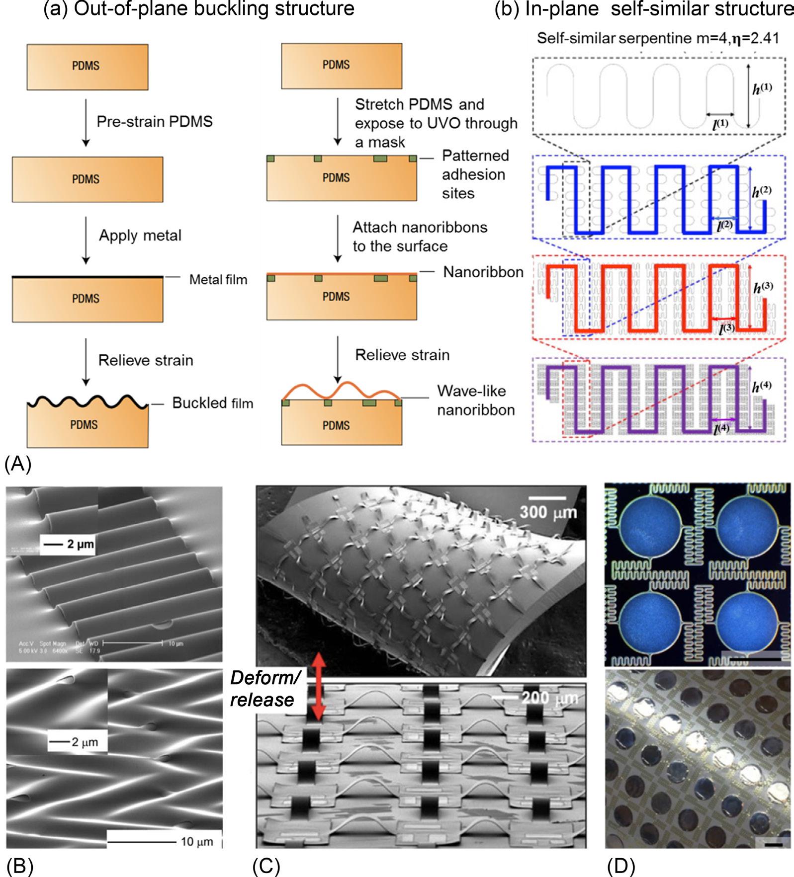
Inorganic electronic materials (e.g., metals and semiconductors) possess outstanding properties as electrodes, sensors, interconnects, contact pads, transistors, and diodes. However, their brittleness makes them tend to fracture under a very little tensile strain (1%), so it is hard to incorporate them directly onto flexible/stretchable substrates [158]. It is reported that once the thickness and size of rigid inorganic materials are reduced to nanometer level, they become deformable and flexible [159]. To achieve tolerance to certain levels of deformation on flexible/stretchable substrate, thin films and special structural configuration design of rigid materials have been developed. Basically, two forms of structural configurations have been widely used: one is out-of-plane buckling structures by compressive buckling strategy (a prestrained substrate during thin film deposition followed by strain release method), including wavy and island-bridge design [158, 160]; the other is in-plane self-similar serpentine or fractal interconnects design [161, 162], as shown in Fig. 1.1A.
Out-of-plane buckling structures are fabricated by compressive buckling strategy, which commonly uses the transfer-printing technique to fabricate a thin film or island-bridge designed mesh layer of inorganic materials on a prestretched elastomeric substrate, and then release of the prestrain leads to formation of wave-like or island-bridge structures on the substrate, as illustrated in Fig. 1.1 A(a). The main difference in the fabrication process of wave-like structure and island-bridge is that the island-bridge mesh is transfer printed onto a prestrained elastomeric substrate with strong chemical bonds at the locations of island (commonly as active area) and weak bonds at the locations of bridge (commonly as interconnect), and when release the prestrain, the bridge buckles out of the plane to accommodate the deformation, while the island experiences very small deformations [163] . However, the thin film layer of wave-like structure is all strongly bonded on the prestrained substrate.
Wavy structure can accommodate external deformations along the prestretched direction (including 1D wavy ribbons layout along one direction and 2D wavy layout in all directions, as shown in Fig. 1.1B) via changing the wavelength (λ) and amplitude (A) in
Materials, systems, and devices for wearable
the waves. Both theoretical and experimental results demonstrate that the wavelength and amplitude of wavy structure are well determined by Eq. (1.1) in small deformation:
See figure legend on next page.
Fig. 1.1
In which hf is the thickness of the rigid film, E f is the Young’s modulus of the film, E s is the Young’s modulus of the elastic substrate, εpre is the prestrain of the substrate, and εc is the critical strain to form wavy structure:
When εpre < εc, no wave forms. Once εpre > εc, wave-like structure will form and according to Eqs. (1.1), (1.2), the wavelengths of the wave-like structure are constant and strain independent. When the prestrain of the elastomeric substrate is relatively large, the wavelength will decrease with the increase of the prestrain [164]. Overall, by varying the material properties (e.g., moduli and thickness) of the rigid film and the compliant substrate, buckling wavy structure systems could be designed with controlled strain direction and level in stretchable electronics applications. Different films such as CNT [165], graphene [166], gold [167], platinum [168], and silver NW [169] are used to fabricate stretchable electronics. Wavy structures provide larger area coverage of active materials on the elastomeric substrate than the island-bridge, which is beneficial for sensors. However, most of them only offer large stretchability in one major direction or small stretchability in all direction on one plane [30]. In addition, the moduli mismatch between rigid film and the elastic substrate, the large strain concentration appearing on the peaks and valleys of the wavy structure could deteriorate the mechanical stability of the electronic device, which are still limitations for certain applications [170].
Fig. 1.1
(A) Structural configuration design strategies of rigid inorganic on stretchable substrate, including (a) out-of-plane buckling structure and (b) in-plane self-similar structure design. (B) Wave-like Si nanomembrane films on a compliant substrate, including 1D sinusoidal wave (upper) for 1D stretch/compression and herringbone wave (below) for 2D stretch/compression. (C) Out-of-plane mesh designs integrated with elastomeric substrate. (D) Al electrode pads and self-similar interconnects on Si wafer (upper) and the transfer printing on a sheet of silicone (below) for a stretchable Li-ion battery. Part (A) reprinted with permission from X. Lu, Y. Xia, Electronic materials: buckling down for flexible electronics. Nat. Nanotechnol. 1 (2006) 163–164 and Y. Zhang, H. Fu, Y. Su, S. Xu, H. Cheng, J.A. Fan, K.-C. Hwang, J.A. Rogers, Y. Huang, Mechanics of ultra-stretchable self-similar serpentine interconnects. Acta Mater., 61 (2013) 7816–7827; (B) reprinted with permission from J. Song, H. Jiang, Y. Huang, J.A. Rogers, Mechanics of stretchable inorganic electronic materials. J. Vac. Sci. Technol. A, 27 (2009) 1107–1125; (C) reprinted with permission from D.-H. Kim, J. Song, W.M. Choi, H.-S. Kim, R.-H. Kim, Z. Liu, Y.Y. Huang, K.C. Hwang, Y.-W. Zhang, J.A. Rogers, Materials and noncoplanar mesh designs for integrated circuits with linear elastic responses to extreme mechanical deformations. Proc. Natl. Acad. Sci. 105 (2008) 18675–18680; (D) reprinted with permission from S. Xu, Y. Zhang, J. Cho, J. Lee, X. Huang, L. Jia, J.A. Fan, Y. Su, J. Su, H. Zhang, H. Cheng, B. Lu, C. Yu, C. Chuang, T.-I. Kim, T. Song, K. Shigeta, S. Kang, C. Dagdeviren, I. Petrov, P.V. Braun, Y. Huang, U. Paik, J.A. Rogers, Stretchable batteries with self-similar serpentine interconnects and integrated wireless recharging systems. Nat. Commun. 4 (2013) 1543.
An island-bridge design has been developed to increase the stretchability of the inorganic electronics comparing to wavy structure, which requires the interconnects (bridge) to be stretchable and suspended out-of-plane, while the island to be rigid, as shown in Fig. 1.1C [160]. The maximum strain in the interconnect is
In which L0 bridge is the distance between islands before relaxation, hbridge is the interconnect thickness, and εpre is the prestrain of the substrate. Eq. (1.3) shows that the maximum strain in the bridge is proportional to the ratio of the interconnect thickness to its length, hbridge/L0 bridge. To increase the stretchability of the interconnects, the maximum strain in the interconnects should be reduced, therefore, thin and long interconnects are preferred. For island, the maximum strain is
In which hisland is the island thickness, visland is the Poisson’s ratio of the island, and Ebridge and Eisland is the Young’s modulus of the interconnect and the island, respectively. Eq. (1.4) shows that stiff and thick island could reduce its strain. As experimental and theoretical studies concluded that long interconnects, short islands, large prestrain could increase both the stretchability and compressibility of the island-bridge system.
To further increase the deformability of the island-bridge system, serpentine interconnects have been developed because they are much longer than straight interconnects. Moreover, serpentine interconnects could be stretched much further when the applied strain reaches the prestrain because structure twist exists to accommodate further deformation. Recently, more advanced 3D out-of-plane buckling design including free-standing helical structure [171], paper folding based spatial structures [64], porous sponge [172], and complex mesostructures [173] have been developed for deformable and stretchable electronics. Within this out-of-plane design, various electronic materials of high moduli can be applied to fabricate stretchable devices, including sensors, energy harvesting, and storage device [51, 174, 175].
Out-of-plane buckling structures can markedly broaden the stretchability and deformability of the flexible electronics. However, the methods involve expensive and complex fabrication processes. Besides, they may easily be broken by scratching from surface, which not suit with well-processed flat technology such as screen printing, lithography in traditional electronics. Therefore, in-plane design of 2D structure would be a good solution for constructing flexible and stretchable electronics. Serpentine structures as a typical in-plane layout have been widely designed and fully fabricated onto elastic substrate as interconnects/electrodes,
which can accommodate an exceptional level of large applied strain without physical damage compared with traditional straight structures [56]. The mechanism to accommodate mechanical strain well is to rationally control the geometric parameters of the serpentine, including wire width, thickness, arc radius and angle, and so on [176]. The systematical simulations and experimental measurements of this structure have been deeply investigated by John Rogers’ group [176, 177]. More advanced in-plane layouts are also developed. For example, a typical self-similar serpentine fractal structure (Fig. 1.1A(b)) shows multiple scale repeated “U”-shaped units [162]. This type of self-similar design expands the lithiumion battery to a biaxial stretchability of up to ~ 300%, which possesses improved level of stretchability compared with traditional networks of periodic serpentine structures with a given spacing between adjacent islands. Moreover, the system can reach even higher stretchability by increasing the fractal order (self-similar orders) of the system, and also can be engineered to accommodate strain along a selected dimension, biaxial, radial, and other deformation modes [46]. These strategies enable thin films of hard electronic materials on flexible and stretchable substrates to be designed for various (bio)electronic devices such as mechanical sensors, radio frequency antennas, heating devices, and so on [178–181]. Future applications lie in broadening the material versatility to other functional materials such as high-quality semiconductors, piezoelectric materials, and 2D layered materials [182]
1.3 Flexible/stretchable sensor devices for wearable bioelectronics
Wearable bioelectronics enables the noninvasive and real-time detection of human physiological information, which mainly includes two categories, one is the physical stimuli signals such as body temperature, heart rate, wrist pulse, respiration, electrophysiological signal (ECG and EEG), and body motions of human activity (subtle movement of face, swallowing and large bending movement of hands, arms, legs, etc.) and the other is biological/chemical stimuli signals, mainly referring to body fluids (sweat, tears, and saliva). For physical signals, plenty of flexible and stretchable physical sensors including pressure/ strain sensors, temperature sensors have been widely developed in the recent years and have shown great application prospects in fitness monitoring, human-machine interfaces, electronic skin (e-skin), and medical diagnostics [4, 29, 65, 183, 184]. Relatively, the developments of (bio)chemical sensors that directly contact with skin for continuous monitoring of biochemical signals are limited, which is due to their complexities in fabrication and performance (molecular level of sensitivity, selectivity, stability of wearable sensors, sample complexity, etc.) [11]. Great efforts have been made to develop wearable flexible and stretchable (bio)chemical sensors in the recent years to obtain more comprehensive, molecular-level information of human body, such as wearable ion-selective electrode sensors, enzyme-based biosensors, wearable microfluidic sensors, and so on. The following part of this chapter will present advanced flexible and stretchable physical and (bio)chemical sensor devices based on the above strategies for wearable bioelectronics.