TerahertzBiomedical andHealthcare Technologies
MaterialstoDevices
Editedby
AMITBANERJEE,PHD
Scientist
MicroelectronicTechnologies & Devices
DepartmentofElectricalandComputerEngineering NationalUniversityofSingapore
Singapore
BASABICHAKRABORTY,PHD
ProfessorandHead
PatternRecognitionandMachineLearningLaboratory DepartmentofSoftwareandInformationScience
IwatePrefecturalUniversity
Japan
HIROSHIINOKAWA,PHD
Professor
DoctorofEngineering
ResearchInstituteofElectronics
ShizuokaUniversity Hamamatsu,Shizuoka,Japan
JITENDRANATHROY,PHD
ProfessorandDean(Science) DepartmentofPhysics
KaziNazrulUniversity
Asansol,WestBengal,India
Elsevier
Radarweg29,POBox211,1000AEAmsterdam,Netherlands TheBoulevard,LangfordLane,Kidlington,OxfordOX51GB,UnitedKingdom 50HampshireStreet,5thFloor,Cambridge,MA02139,UnitedStates
Copyright 2020ElsevierInc.Allrightsreserved.
Nopartofthispublicationmaybereproducedortransmittedinanyformorbyanymeans,electronicor mechanical,includingphotocopying,recording,oranyinformationstorageandretrievalsystem,without permissioninwritingfromthepublisher.Detailsonhowtoseekpermission,furtherinformationaboutthe Publisher’spermissionspoliciesandourarrangementswithorganizationssuchastheCopyrightClearance CenterandtheCopyrightLicensingAgency,canbefoundatourwebsite: www.elsevier.com/permissions
ThisbookandtheindividualcontributionscontainedinitareprotectedundercopyrightbythePublisher(other thanasmaybenotedherein).
Notices
Knowledgeandbestpracticeinthis fieldareconstantlychanging.Asnewresearchandexperiencebroadenour understanding,changesinresearchmethods,professionalpractices,ormedicaltreatmentmaybecome necessary.
Practitionersandresearchersmustalwaysrelyontheirownexperienceandknowledgeinevaluatingandusing anyinformation,methods,compounds,orexperimentsdescribedherein.Inusingsuchinformationormethods theyshouldbemindfuloftheirownsafetyandthesafetyofothers,includingpartiesforwhomtheyhavea professionalresponsibility.
Tothefullestextentofthelaw,neitherthePublishernortheauthors,contributors,oreditors,assumeany liabilityforanyinjuryand/ordamagetopersonsorpropertyasamatterofproductsliability,negligenceor otherwise,orfromanyuseoroperationofanymethods,products,instructions,orideascontainedinthe materialherein.
LibraryofCongressCataloging-in-PublicationData
AcatalogrecordforthisbookisavailablefromtheLibraryofCongress
BritishLibraryCataloguing-in-PublicationData
AcataloguerecordforthisbookisavailablefromtheBritishLibrary
ISBN:978-0-12-818556-8
ForinformationonallElsevierpublicationsvisitourwebsiteat https://www.elsevier.com/books-and-journals
Publisher: MatthewDeans
AcquisitionsEditor: KaylaDosSantos
EditorialProjectManager: MarianaC.Henriques
ProductionProjectManager: SreejithViswanathan
Coverdesigner: MilesHitchen
TypesetbyTNQTechnologies
Contributors
AmitBanerjee,PhD Scientist
MicroelectronicTechnologies & Devices DepartmentofElectricalandComputerEngineering NationalUniversityofSingapore
Singapore
SouravBanerjee,PhD AssistantProfessor
KalyaniGovernmentEngineeringCollege Kalyani,WestBengal,India
SuranjanaBanerjee,PhD,MTech,BTech,BSc Electronics DumDumMotijheelCollege Kolkata,WestBengal,India
Electronics & TelecommunicationEngineering IndianInstituteofEngineering Science & Technology Kolkata,WestBengal,India
TanmoyBasu,PhD ResearchFellow CentreforAdvanced2DMaterials NationalUniversityofSingapore
Singapore CentreforIonBeamApplications DepartmentofPhysics NationalUniversityofSingapore
Singapore
NurniharBegum,PhD ResearchScholar DepartmentofEngineering & TechnologicalStudies UniversityofKalyani Kalyani,WestBengal,India
BasabiChakraborty,PhD ProfessorandHead PatternRecognitionandMachineLearningLaboratory DepartmentofSoftwareandInformationScience IwatePrefecturalUniversity
Japan
ChinmayChakraborty,PhD Doctor
BirlaInstituteofTechnology Electronics & CommunicationEngineering Deoghar,Jharkhand,India
SulagnaChatterjee,MSc,MTech,PhD(Tech) AdamasUniversity Kolkata,WestBengal,India
DebashisDas,MTech StudentMember KalyaniGovernmentEngineeringCollege Kalyani,WestBengal,India
SubalKar,MTech,PhD(Tech) FulbrightScholar,FormerProfessorandHead InstituteofRadioPhysicsandElectronics UniversityofCalcutta Kolkata,WestBengal,India
BrightKeswani,PhD Professor DepartmentofComputerApplications SureshGyanViharUniversity Jaipur,Rajasthan,India
PoonamKeswani,PhD AssistantProfessor AkashdeepPGCollege Jaipur,Rajasthan,India
IlyaKrasnikov,PhD DepartmentofPhysics AmurStateUniversity Blagoveshchensk,Russia HannoverCentreforOpticalTechnologies Hannover,Germany
YogeenthKumaresan,PhD SchoolofMaterialsScienceandEngineering GwangjuInstituteofScienceandTechnology Gwangju,RepublicofKorea
AshisKumarMandal DepartmentofSoftwareandInformationScience IwatePrefecturalUniversity Morioka,Japan
AmbarishG.Mohapatra,PhD SeniorAssistantProfessorandHead DepartmentofElectronicsandInstrumentation Engineering SiliconInstituteofTechnology Bhubaneswar,Odisha,India
RahulMondal,PhD ResearchScholar DepartmentofEngineering & TechnologicalStudies UniversityofKalyani Kalyani,WestBengal,India
M.Mukherjee,MSc,MTech,PhD(Tech),PDF AdamasUniversity Kolkata,WestBengal,India
NileshMukherjee,PhD ResearchScholar DepartmentofEngineering & TechnologicalStudies UniversityofKalyani Kalyani,WestBengal,India
YutakaOyama,PhD TohokuUniversity Sendai,Japan
PraveenKumarPoola,PhD ElectronicsandCommunicationEngineering KLHDeemedtobeUniversity Off-campusHyderabad Hyderabad,Telangana,India
SrinivasaRaoRagam,PhD AdvanceMaterialsandDeviceMetrology CSIR-NationalPhysicalLaboratory NewDelhi,India
MeghaRathi,Sr.,PhD Doctor
DepartmentofComputerScience & IT,Jaypee InstituteofInformationTechnology Noida,UttarPradesh,India
P.SoniReddy,PhD ResearchScholar DepartmentofEngineering & TechnologicalStudies UniversityofKalyani Kalyani,WestBengal,India
ParthaPratimSarkar,PhD Professor DepartmentofEngineering & TechnologicalStudies UniversityofKalyani Kalyani,WestBengal,India
SushantaSarkar,PhD AssistantProfessor DepartmentofEngineering & TechnologicalStudies UniversityofKalyani Kalyani,WestBengal,India
RiktaSen DepartmentofSoftwareandInformationScience IwatePrefecturalUniversity Morioka,Japan
AlekseiSeteikin,PhD AssociateProfessor DepartmentofPhysics AmurStateUniversity Blagoveshchensk,Russia DepartmentofFundamentalandAppliedPhotonics ImmanuelKantBalticFederalUniversity Kaliningrad,Russia
SaumitraVajandar,PhD CentreforIonBeamApplications DepartmentofPhysics NationalUniversityofSingapore
Singapore
LokeshVijay,MBBS ConsultantSurgery DelhiMultiSpecialtyHospital Delhi,India
PrityVijay,PhD
DataScientist
ZesstaSoftwarePrivateLimited
Hydrabad,Telangana,India
PuZhao,PhD
LehighUniversity
Pennsylvania,PA,UnitedStates
Thorlabs
Shanghai,China
AbouttheEditors
Dr.AmitBanerjee
Scientist,MicroelectronicTechnologies & Devices, DepartmentofElectricalandComputerEngineering, NationalUniversityofSingapore, Singapore
Email:amitbanerjee.nus@gmail.com;eleami@nus. edu.sg
ShortBiography:AmitBanerjeejoinedtheAdvanced DeviceResearchDivision,ResearchInstituteofElectronics,NationalUniversityCorporation,Japan,asa ScientificResearcherin2016andwasalsopartofthe InnovativePhotonicsEvolutionResearchCenterat Hamamatsu,Japan.HelaterjoinedtheMicroelectronic Technologies & Devices,DepartmentofElectricaland ComputerEngineeringoftheprestigiousNational UniversityofSingapore,asScientistin2017.Currently, Amitisamemberof30þ internationaladvisoryboards, technicalprogramcommitteesinvariouscountries, actedaspaneleditor,reviewerforreputedjournalsand scientificbookvolumes,memberofJapanSocietyof AppliedPhysics,IndianPhysicalSociety;External Adviser,BioelectronicsandBiomedicalTechnologies, OcuroScienceandTechnology(Biomed-startup); AdviserandLeadContributor:SemiconductorDevices andProcessTechnologies,EDGE196,Entrepreneur
DevelopmentGlobalEcosystem;Adviser,Entrepreneurs Face,Singapore,GlobalVentureCapitalandEntrepreneursNetwork,Singapore;TechnicalAdvisertoULVAC Technologies;amongvariousothers.Amithascoauthoredseveralscientificpapers,editedbooks,presented inseveralinternationalconferencesasplenaryand keynotespeakers,receivedawardsincludingyoung physicistawardandhonorarylife-membershipfrom IndianPhysicalSociety,awardbytheMetrologySociety ofIndia,IndianInstituteofChemicalEngineers,award byDepartmentofAtomicEnergy,hisworkonnanodiamondswasalsoawardedandfeaturedasakeyscientificarticlecontributingtoexcellenceinengineering, scientific,andindustrialresearch,byAdvancesinEngineering,USA;recently,theirworkrelatedtoon-chip integrableterahertzdetectorswasawardedbyQuality inResearch,Indonesia,alongwithProfessorHiroshi Inokawa,RIE,Japan.Alongsidethepursuitofresearch andadministrativeambitions,Amitiskeenlyengaged inconsultingfuturistictechnologiesforbusiness firms, educationalventures,anduniversities.Amitreceived PhDdegreeinSemiconductorTechnologyfromEnergy ResearchUnit,IndianAssociationfortheCultivationof Science(GovernmentofIndia),andextensivelyworked ondesignanddevelopmentofhighvacuumplasma CVDreactors,whichareusedinindustrialmanufacturingofsolarcells,coatings,andTFTs.Healso developedlow-costhighvacuumMW-PECVDunitsand conceivedtheprocessforcost-effectivecommercial gradeantireflectioncoatingsynthesisforsolarcellsby nanocrystallinediamonds.HiscurrentworkisonTerahertzTechnology,includingTHzsensorsandsources, design,andfabrication,aimingatbiomedicalimaging applications.Hisrecentworkonantenna-coupled microbolometerarraysiscompatiblewiththestate-ofthe-artmedium-scalesemiconductordevicefabrication processesandtechnologicallycompetitivewithcommercialviabilityason-chipintegrabledetectorarraysfor terahertzimaging.

Dr.BasabiChakraborty
ProfessorandHead,PatternRecognitionandMachine LearningLaboratory FacultyofSoftwareandInformationScience,Iwate PrefecturalUniversity,Japan
Email:basabi@iwate-pu.ac.jp
ShortBiography:BasabiChakrabortyreceivedB.Tech, M.Tech,andPhDdegreesinRadioPhysicsandElectronicsfromCalcuttaUniversity,India,andworkedin IndianStatisticalInstitute,Calcutta,India,until1990. From1991to1993,sheworkedasapart-time researcherinAdvancedIntelligentCommunication SystemsLaboratoryinSendai,Japan.Shereceived anotherPhDinInformationSciencefromTohoku University,Japan,in1996.From1996to1998,she workedasapostdoctoralresearchfellowinResearch InstituteofElectricalCommunication,TohokuUniversity,Japan.In1998,shejoinedasafacultyinSoftware andInformationScienceDepartmentofIwatePrefecturalUniversity,Iwate,Japan.Currently,sheisservingas ProfessorandHeadofPatternRecognitionandMachine LearningLaboratoryinthesamedepartment.Hermain researchinterestsareintheareaofPatternRecognition, MachineLearning,SoftComputingTechniques,Biometrics,DataMining,andSocialMediaDataMining. SheisaseniormemberoftheInstituteofElectricaland ElectronicsEngineers(IEEE),memberofACM,Japanese NeuralNetworkSociety,JapaneseSocietyofArtificial Intelligence,andexecutivecommitteememberofISAJ (IndianScientistsAssociationinJapan).Sheservedas thechairofIEEEJCWIE(WomeninEngineering)during2010 2011.Shealsoservedasthefounderchairof IEEEWIESendaisectionduring2017 2018.Currently, sheisexecutivecommitteememberofIEEER10WIE, IEEEJCWIE,andSendaiWIE.

Dr.HiroshiInokawa
Professor
ResearchInstituteofElectronics, ShizuokaUniversity
Hamamatsu,Japan
Email: inokawa.hiroshi@shizuoka.ac.jp
ShortBiography:HiroshiInokawareceivedBS,MS, andPhDdegreesinelectricalengineeringfromKyoto University,Japan,in1980,1982,and1985,respectively.In1985,hejoinedtheAtsugiElectricalCommunicationsLaboratories,NipponTelegraphand TelephoneCorporation(NTT),Kanagawa,Japan.Since then,hehasbeenengagedintheresearchanddevelopmentofscaled-downCMOSdevicesandsilicon single-electrondevices.Duringthecourseofhis research,heinventedthebasicstructureofFinFETin 1989andsingle-electronmultiple-valuedlogicin2001 andreceivedIEEEInternationalSymposiumon Multiple-ValuedLogicOutstandingContributedPaper Awardsin2004and2006,Director’sAwardofNTT BasicResearchLaboratoriesin2004,28thJSAPAward fortheBestOriginalPaperin2006,etc.In2006,he becameaprofessoroftheResearchInstituteofElectronics,ShizuokaUniversity,Hamamatsu,Japan, wherehehasbeenstudyingnanodevicesforadvanced circuitsandsystems.HisrecentworkonSOIMOSFET single-photondetectorwasintroducedbyIEEEPhotonicsJournalin2012asaBreakthroughinPhotonics. ProfessorInokawaisamemberofIEEE,theJapan SocietyofAppliedPhysics(JSAP),theInstituteof Electronics,InformationandCommunicationEngineersofJapan,andtheInstituteofElectricalEngineers ofJapan(IEEJ).HehasservedasaJSAPboardmember ofrepresentativein2001 03,aneditorofJJAPin 2007 13,thechairoftheIEEJsurveycommitteeof
siliconnanosystemintegrationtechnologyin 2009 11,anadvisorycommitteememberofNICT JapanTrustInternationalResearchCooperation Programin2006 09,aresearcherofNationalInstitute ofScienceandTechnologyPolicyin2002-present,etc.
Dr.JitendraNathRoy ProfessorandDean(Science) DepartmentofPhysics, KaziNazrulUniversity,CHKalla, Asansol,WestBengal,India
Email: jnroys@yahoo.co.in
ShortBiography:JitendraNathRoyreceivedMScand PhDdegreeinPhysicsfromVidyasagarUniversity, India.HehadjointresearchprogramatDepartmentof ElectricalandComputerEngineering,LightWave CommunicationsResearchGroup,Xanthi,Greece. ProfessorRoyreceivedInternationalSardarPatel AwardfromSardarVallabhbhaiPatelFoundationfor significantcontributioninphysicalscience.Dr.Royhas 20yearsofexperienceinteachingresearchand administration.Presently,Dr.Royisworkingasa ProfessorandDean(science)inDepartmentofPhysics atKaziNazrulUniversity,Asansol,WB,India.Hehas alreadypublishedmorethan123researchpapersin peer-reviewedjournalsandconferenceproceedings.Dr. RoyreceivedresearchgrantfromAICTE,Government ofIndia,underFRSSchemeforresearchin “Designing ofanall-opticalconversionschemefrombinarytoits ModifiedTrinaryNumber.” Dr.Royismemberof manyInternationalAdvisoryCommittees,Technical ProgramCommitteesinvariouscountries,actedas PanelEditor,Reviewerforreputedjournals.Professor RoyhasproducedninePhDstudentsindifferenttopics ofappliedopticsandphotonics,linearandnonlinear opticalmaterial,andlaser.Hiscurrentresearchinterest isinTerahertzOpticalAsymmetricDemultiplexerbasedswitchinComputing,Communication,and Control.
THzSolid-StateSourceBasedon IMPATTDevices
SURANJANABANERJEE,PHD,MTECH,BTECH,BSC
INTRODUCTION
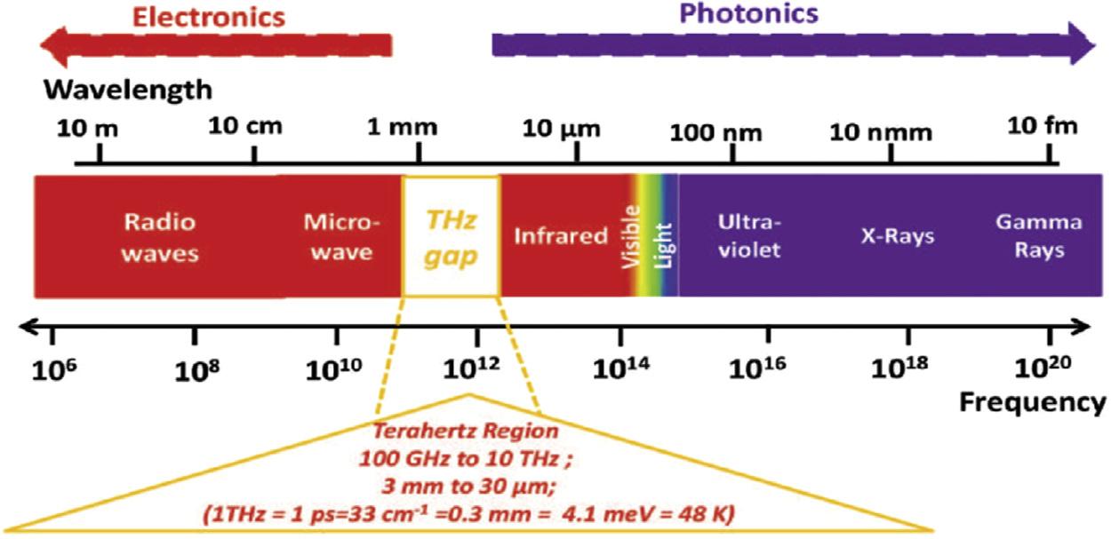
Theterahertz(THz)regionoftheelectromagneticspectrumliesbetweenthetraditionalmillimeterwaveand opticalbandsinthefrequencyrangeof0.1 10THz andwavelengthrangeof3 0.03mm.Itisalsopopularly called “THzgap” lyingbetweenmicrowaveandinfrared frequencybandasshownin Fig.1.1.THzscienceand technologyareattractingtheattentionofresearchersin recenttimesmainlyduetotheemergenceoftimedomainspectroscopyusingpulselaserofextremely narrowwidthassources.Theresearchersarenowable tocarryouttime-resolved “far-infrared” studiesand explorespectroscopyandimagingapplicationsinthe THzfrequencyregime.
THztechnologycanbeusedininformationscience, biology,medicine,astronomy,andenvironmental science.THzsourceshavenumerousapplicationsin surveillance,bioterroristattack,andpathogendetection whereTHzwaveisusedtodetectairborneanthrax particles.SomeofTHzsemiconductorsourcesare GaAs1 xNx-basedGunn-likediodes,quantumwell (QW),negativeeffectivemass(NEM)oscillators,and quantumcascadelasers(QCLs).THzcurrentoscillation indopednþnnþ GaAs1 xNx diodesdrivenbyDCelectric fieldhasbeentheoreticallystudiedbyFengandCao[1]. Self-oscillationisassociatedwiththenegativedifferential velocityeffectinthehighlynonparabolicconduction bandofthisuniquematerialsystem.Theyobserved thatimpurityandphononscatteringmechanismsare responsibleforcurrentself-oscillationinQWNEM pþppþ diodes.TheNEMpþppþ diodemaybeusedas anelectricallytunableTHzsource.The firstTHzQClaser withphotonenergylessthanthesemiconductoroptical phononenergywasdemonstratedat4.4THz.Theoptimizationofdeviceparametersofresonant-phonon THzQCLscanbedonebyusingMonteCarlomethod.
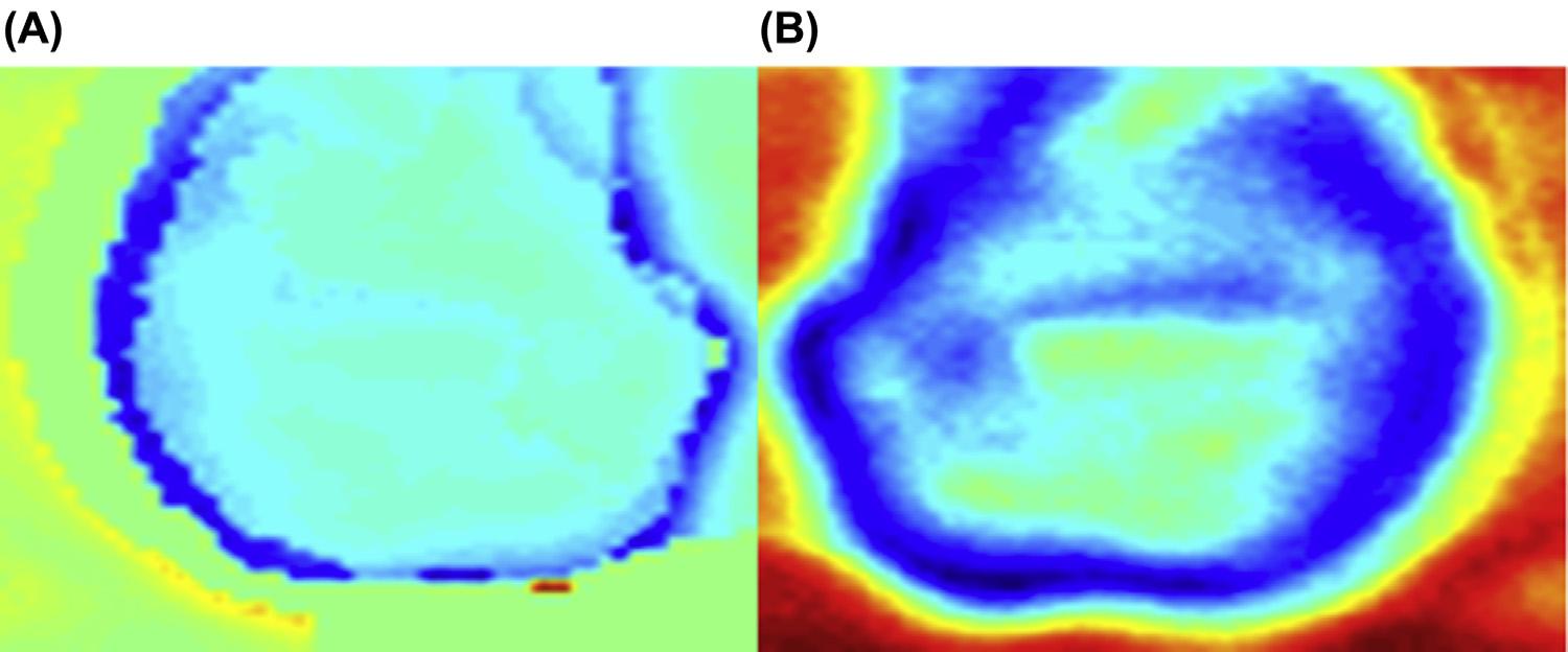
Alotofresearchinteresthasgeneratedforthe researchanddevelopmentofTHzcomponents,sources, anddetectorsduetotheirvariousapplicationsin astronomy,spectroscopy,bioimaging,biosensing,qualityinspectioninindustrialproducts,andmedicaland pharmaceuticalresearchareas.Bioimagingusingtera rayshowsbetterresolutionofcarcinomacellsinhuman bodyascomparedwiththatusingX-ray(Fig.1.2).
Inrecentyears,thedevelopmentofTHzsolid-state sourcewithappreciablepowerisattractingtheattention ofresearchersduetotheirimportantapplicationsin shortrangeterrestrialandairbornecommunication andspace-basedcommunication.SomeoftheTHz sourcesreportedintheliteratureareelectronbeam, opticallypumpedfar-infraredgaslasers,semiconductor QCLs,resonanttunnelingdiode,TUNNETTdiode,and Gunndiode.
Recently,cascadedfrequencymultipliershavebeen reportedwhichcangenerate10 2 mWpowerat 1.9 2.7GHzforapplicationaslocaloscillatorsinan astronomicalreceiver.However,somesemiconductor devicessuchasQCLs,highelectronmobilitytransistors, andheterojunctionbipolartransistorshaveemergedas potentialsourcestogenerateTHzsignals.ThesesolidstatesourcescanbetunedtoappropriateTHzfrequency at300K.Butthepowergeneratedbythesesourcesat THzisnothighenoughtousetheminthetransmitter sectionofthesystem.ThegenerationofTHzsignal withappreciablepowerisindeedachallengingareaof research.Theresearchersarethereforeexploringto searchforanalternativesolid-statesourceatTHzfrequencybandwhichshouldbecompact,cost-effective, efficient,andpowerful.Inthisrespect,thedevelopment ofimpactavalanchetransittime(IMPATT)devices basedonwidebandgap(WBG)semiconductorlike GaNisworthwhiletonote.
POTENTIALTHZSOLID-STATESOURCE USINGIMPATTDIODES
Varioussolid-statesourcesareavailableforgeneration ofRFpoweratmicrowaveandmillimeterwavefrequencybands.Amongthesesources,IMPATTand mixedtunnelingtransittime(MITATT)deviceshave alreadyemergedashigh-power,highefficiencysolidstatesourcesbothatlowermicrowave(3 30GHz) andhighermm-waveandsub-mm-wave (30 300GHz)frequencybands.Mostoftheresearch activitiesformm-wavesystemsusingIMPATTsources areconcentratedonwindowfrequencies,i.e.,35,94, 140,and220GHz,whereatmosphericattenuationis relativelylow.
IMPATTdevicesbasedonSiarereportedtoprovide highpoweratdifferentmm-wavewindowfrequencies [2,3].Althoughthesedeviceshavebeenrealizedat lowermicrowaveandhighermm-wavefrequency bands,nosignificantprogresshasyetbeenreportedto
practicallyrealizethissourceforoperationatTHz frequencies.Inrecentyears,thepotentialityofIMPATT devicesbasedonWBGsemiconductingmaterialssuch asSiC,GaN,andtype-IIbdiamondashigh-power sourceshasbeenreportedatTHzfrequencies[4 10]. Thischapterwillprovideacomprehensivereviewon thephysicalphenomenaresponsibleforgenerationof THzwavefromIMPATTdevicesandthedesignand developmentofthesedevicesascompact,low-cost, efficient,andpowerfulTHzsources.
TheBasicConceptsofIMPATTOperation
IMPATTdevicesarebasicallyreversebiasedp-njunctiondiodesoperatedatavalanchebreakdownvoltage. Embeddedinaresonantcavity,theyexhibitoscillation atmicrowaveandmillimeterwavefrequenciesto generatepower.Thesedevicesexcelmetalsemiconductor fi eld-effecttransistors(MESFETs)andGunn diodesintermsofoutputpower,DCtoRFconversion
FIG.1.1 Terahertzregion.
FIG.1.2 (A) X-rayview, (B) teraview.
ef fi ciencyathighermm-wavefrequencies.Thesedevicesarehighlyattractiveandreliablesourcesfor mm-wavepowergenerationduetotheirwidefrequencycoverage,high-poweroutputandhighconversionef fi ciencycoupledwithtuningcapability,low cost,andsimplecircuitarrangement.They fi ndwide applicationsinsatellitecommunicationsystems, trackingradarsandmissileguidanceforbothcivilian anddefenseapplications.
In1954,Shockley[11 ]showedthatthetransittime (TT)delayofanelectronbunchinaforwardbiasedp-n junctiondiodeisresponsibletoproducenegative resistanceatmicrowavefrequencies.Theoriginof negativeresistanceinIMPATTdeviceisideallyaphase lagof180 betweentheinputRFvoltageandexternal current.Underavalanchebreakdowncondition,the phenomenaofimpactionizationandavalanchemultiplicationinthedepletionlayerofthedevicegiverise toanavalanchephasedelayof90 .Thecarriers injectedfromtheavalanchelayerrequirea fi niteTT tocrossthedriftlayerandarriveattheterminalwhich introducesanotherdelaycalledTTdelay.Whenthe avalanchedelayaddedtoTTdelayisequaltohalfcycletime,thedioderesistancebecomesnegativeat thecorrespondingfrequency.W.T.Readin1958 [ 12]showedthatthecombinedeffectsofavalanche andTTdelayinareversebiasedpþ-ninþ diodeunder avalanchebreakdownproducesanappropriatephase delayof180 betweeninputvoltageandexternalcurrenttoproducenegativeresistanceatmicrowave frequencies.Johnsonetal.[13 ]in1965 fi rstobserved microwaveoscillationfromasimplepþnnþ device.T. Misawa[ 14 ]showedfromsmall-signalanalysisthe existenceofnegativeresistanceofanavalanchediode ofarbitrarydopingpro fi le.
CommerciallyavailablemillimeterwaveIMPATTs aremostlybasedonSiduetomaturedprocessingtechnologyofSi.AlthoughIMPATTsmadeofGaAsarealso practicallyrealized,theavailablereportsindicatethat theirRFperformanceasregardhigh-powerdelivery withhighconversionefficiencyislimitedabove 50GHz.IMPATTsbasedonInPand4H-SiChave beendesignedandfabricated.WBGsemiconductors like4H-SiC,GaN,andtype-IIBdiamondshowgreat promiseasbasesemiconductorsforfabricationof IMPATTs,MITATTs,andTUNNETTsathighermillimeterwaveuptoTHzfrequencybands[4 8,15,16]. FurtherIMPATTsbasedonheterojunctionsofGr. IV-IVandGr.III-Vsemiconductorsarereportedtobe usefulsourcestodeliversufficientpowerwithlownoise levelatsub-mm-wavefrequenciesabove100GHz.
Significantprogressinoutputpowerandefficiency hasbeenachievedwithIMPATTdiodesandoscillators atfrequenciesfrom30to300GHzoverthepast decades.SiliconIMPATTshaveemergedaspremier solid-statesourcesofRFpowerinbothcontinuous wave(CW)andpulsedmodesofoperationatmmwavefrequencybands.Flatprofilesingledriftand double-driftsiliconIMPATTsoperatingintheCW modehaveproducedoutputpowersof2.25Wat 40GHz,600mWat94GHz,110mWat140GHz, 50mWat220GHz,and1.2mWat301GHz.Similarly, pulsedoutputpowersof23Wat35GHz,42Wat 96GHz,3Wat140GHz,and520mWat220GHz havebeenreported[17,18]fromsiliconIMPATT devices.Above50GHz,theRFperformanceofSi IMPATTsexcelsthatofGaAsIMPATTs.Someefforts havebeenmadetoimprovetheperformanceofGaAs IMPATTsatmm-waveV-band(60GHz)andW-band (94GHz)frequenciestakingtheadvantagesof improveddevicedesignandprocesstechnology.
ApartfromSiandGaAsIMPATTs,indiumphosphideIMPATTshavebeenrealizedprovidinggoodRF performanceatX-andV-bands.J.J.Berenzetal.in 1978[19]reportedthefabricationofsingledriftpþnnþ structureofInPIMPATTsbyion-implantationtechniqueandshowedthatthedevicesprovideaCWpower of1.6Wwith11.1%efficiencyat9.78GHz.Vassilevsky etal.andYuanetal.[8,20]reportedfabricationof singledriftregion(SDR)IMPATTsbasedon4H-SiC with flatandhigh-lowdopingprofileatX-andKubands,respectively.Amaximumoutputpowerof 300mWandbreakdownvoltageof290Vwasreported fromthesedevicesatabiascurrentdensityof 0.95 107 Am 2.Thehighbreakdown fieldandelectronsaturationvelocityofSiCisideallysuitedtofabricatehigh-powerIMPATTsfromthissemiconductor.The power-frequencyproduct(pf2)ofIMPATTdiodeisproportionalto(EmVsn)2.Thebreakdown fieldorcritical fieldofSiCisabout10timeshigherthanthatofSior GaAsandthesaturationvelocityisabout2times higher.Thus,thepower-frequencyproduct(intheelectroniclimit)ofSiCIMPATTsisexpectedtobe400times higherthanSiorGaAsIMPATTs.
PracticalIMPATTdiodesareintermediatebetween ReadandMisawadiodesinthesensethattheavalanche zoneiswelldefined,neithertoothinnortoowide.The avalanchechargepulseisinjectedfromawell-defined avalanchezoneintothedriftzoneapproximately90 behindtheRFvoltageandtheinjectedchargetravels withasaturateddriftvelocityinthedriftregion.The SDRIMPATTdiodehavingpþnnþ structureand
double-driftregion(DDR)IMPATTdiodehaving pþpnnþ structurearemostlyusedaspracticalstructures ofthedevice.
SomeLandmarksintheDevelopmentof IMPATTs
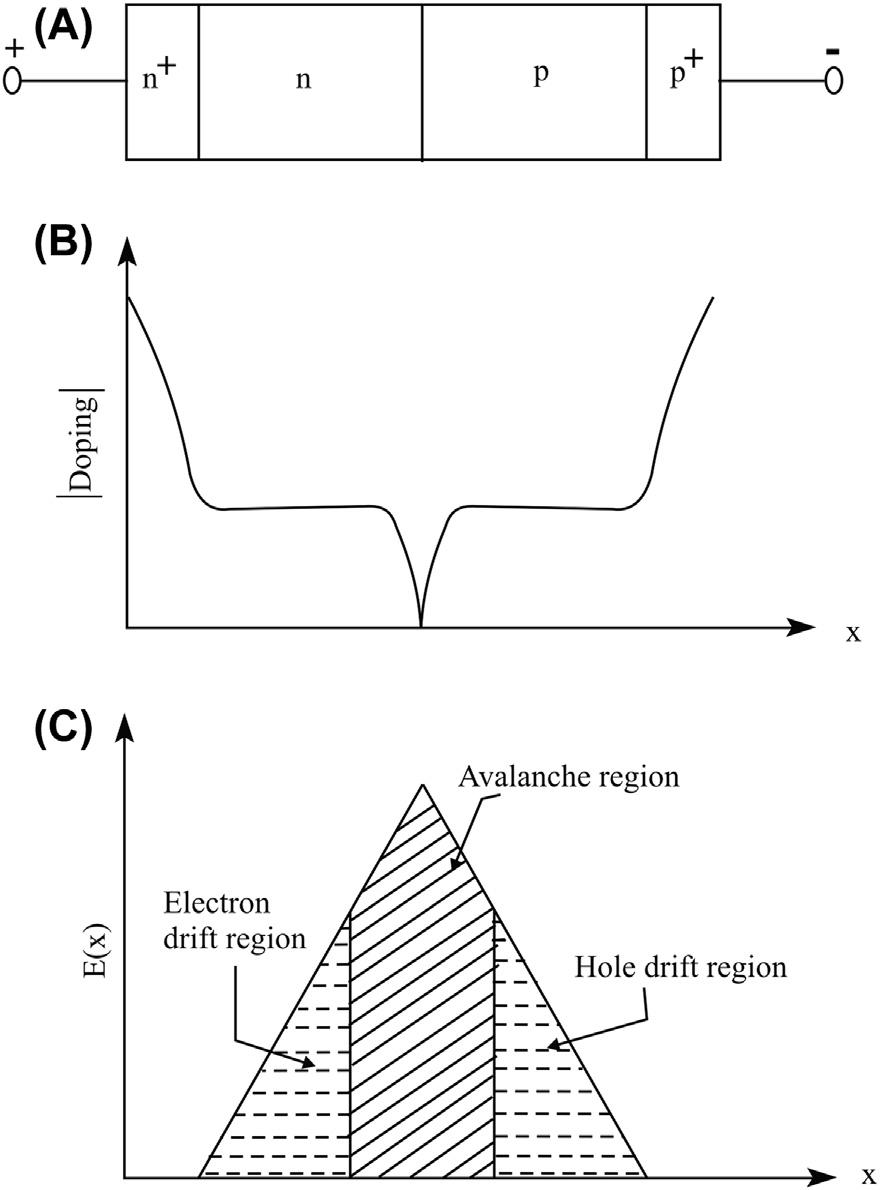
The fi rsteverpracticalstructureofIMPATTsrealized experimentallyisSDR pþ-n-nþ/n þ-p-pþ structurewith aSDRforelectronsorholesandanavalancheregion ofnarrowwidthlocatedatoneendofthedepletion layernearthemetallurgicaljunction.Schematicdiagramsofthestructure,dopingpro fi le,andelectric fi eld pro fi leatbreakdownofpþnn þ SDRIMPATTdiodeare shownin Fig.1.3A C ,respectively.The fi eldpro fi le shownin Fig.1.3C indicatesthatthedeviceisjust punchedthroughatoperatingtemperatureandthe avalanchezonewidthisafractionofthedepletion layerwidth.Flatpro fi leSDRIMPATTdiodesusing Si/GaAs/InP/4H-SiCasbasesemiconductorshave beenexperimentallyrealized.Apunchedthrough structureofIMPATTdiodeavoidspositiveresistance duetoundepletedepitaxy.Itmaybenotedinthis contextthatSDRp þnnþ structureofSiIMPATTsisbetterthanitscomplementarynþppþ structuresofaras highpowerdeliveryfromthedeviceisconcerned.
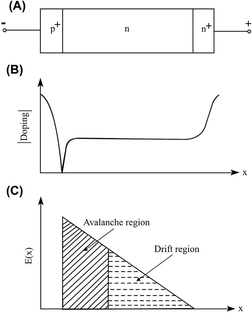
FIG.1.3 (A) Singledriftregion(SDR)IMPATTdiode structure, (B) dopingprofileand (C) fieldatbreakdown showingtheavalancheanddriftregions.
ADouble-DriftRegion(DDR)structure(pþ-p-n-nþ) ofIMPATTswithtwodriftregions,oneforelectrons andanotherforholesoneithersideofacentral avalancheregion,was firstproposedbyScharfetter etal.[21]in1970.Inthistypeofstructure,bothelectronsandholestakepartequallytodelivermicrowave powerwhiledriftinginoppositedirectionsthrough twodriftregionsoneithersideofthecentralavalanche region.Itisquiteevidentthattwodriftregionsinthe caseofDDRIMPATTdiodesshouldprovidehigher outputpower,higherefficiency,andhigherimpedance perunitarea,comparedwithSDRIMPATTdiodein whichmicrowavepoweriscontributedbythedriftof onlyonetypeofcarrier,eitherelectronorhole.DDR structureofIMPATTdiodeperformsbetterthanits SDRcounterpartnotonlywithrespecttoRFpower outputbutalsowithrespecttoDCtoRFconversion efficiency.DDRIMPATTdiodeiscapableofdelivering bothhigh-powerandhigh-efficiencyatmmand sub-mm-wavefrequencybands.Theschematicdiagramsofthestructure,dopingprofile,and fieldprofile ofDDRnþ-n-p-pþ IMPATTdiodeareshownin Fig.1.4A C,respectively.Ahigh fieldavalancheregion locatedcentrallynearthemetallurgicaljunctionand twolowrelativelylow fielddriftregionsoneitherside oftheavalanchezoneconstitutetheactiveregionofa DDRIMPATTdiode.Inthecentralavalanchezone,carriersaregeneratedbyimpactionizationduetosufficientlyhigh fieldintheavalanchelayer.
TheequivalentcircuitofIMPATTdevicemaybe consideredtoconsistofanegativeresistance RD in serieswithareactance XD,where RD isusuallysmall comparedwith XD .Thewidthoftheactiveregion ( W)DDRstructureislargerthanthatofSDRstructure ofIMPATTdioderesultinginasmallercapacitance
C ¼ ˛A W andhencealargercapacitivereactanceper
unitarea Xc ¼ 1 jwc ofthedevice.ThepowerfrequencyproductofanIMPATTdiodeisaconstant athighermillimeterwavefrequencies.Theimpedance andthebreakdownvoltageofDDRIMPATTsareboth almostdoublethatofSDRIMPATTs.Theareaofthe DDRdevicecanbeincreasedtomaintainthesame valueofcapacitivereactanceasthatofcomparable SDRdevice,inordertoderivemaximumoutputpower fromDDRdiode.Simultaneously,theincreasedarea reducestheseriesresistanceassociatedwithn þ and pþ contactregions.Alsothedegradationofef fi ciency duetotheeffectofminoritycarrierstorageisnot signi fi cantinaDDRdiodebecausetheavalanche zoneiscentrallylocated.
FIG.1.4 (A) Double-driftregion(DDR)IMPATTdiode structure, (B) dopingprofile,and (C) Fieldatbreakdown showingtheavalancheanddriftregions.
AccordingtoScharfetter-Gummelformula,theDC toRFpowerconversionefficiencyofaDDRIMPATT diodeisgivenby h ¼ 1 p VD 1 þ VD VA (1.1)
where VA and VD arethevoltagedropsacrossthe avalancheanddriftzonesofDDRdiode.Theratioof driftregionvoltagedrop(VD)toavalanchezonevoltage dropishigherinDDRdiodeascomparedwiththatin SDRdiodewhichleadstohigherconversionefficiency ofDDRIMPATTdiode.
Themagnitudeofpeakelectric fieldatthep-njunctionofDDRdiodeislessthanthatofSDRdiodeunder identicaloperatingconditions.Further,thedepletion regionofaDDRdiodeiswiderthanthatofanSDR diode.Theeffectoftunnelingofchargecarriersonthe high-frequencypropertiesofDDRdeviceislesspronouncedsincethedepletionlayerwidthiswiderin DDRdiode.Scharfetteretal.[21] firstdemonstrated mm-wavepowergenerationfromexperimental flat
profileDDRSiIMPATTdiode.Seideletal.in1971 [22]reportedthatanion-implanted flatprofileDDR SiIMPATTdevicedelivershighCWoutputpowerof 1Wat50GHzwith14.2%conversionefficiency.A CWpowerof0.53Wwith10.3%conversionefficiency atthesamefrequencywasreportedbythesameworker [22]fromcorrespondingSi flatprofileSDRdiode.Later severalresearchersconfirmedthesuperiorityofDDR diodesovertheirSDRcounterpartsatbothmicrowave andmm-wavefrequencies.
HETEROJUNCTIONIMPATTDIODE
Theconductionbanddiscontinuitypropertiesofabrupt heterojunctionsformedbetweentwosemiconductorsof differentbandgaps,incorporatedinIMPATTstructure, leadtoimprovedRFperformanceofthedeviceathigher mm-wavefrequencybands.Theimportantfeatureof HJ-IMPATTisthesharpnessofthepeakelectric fieldat thejunction.Theuseofaheterojunctioninplaceof theconventionalp-njunctioninanIMPATTstructure leadstoitssuperiorDCcharacteristics,betterRFproperties,andlessphasenoise[23 25].Forgivendoping levels,andassumingnointerfacecharge,themaximum fieldattheinterfaceisfoundtobelargerinaheterojunctionbasedonGaAs/Al0.3GaAs0.7 thanthatinastandard GaAsp-nhomojunction[26,27].Theavalanche noisecharacteristicsofInP/GaInAs(Ga0.47 in0.53 As) andInP/GaInAsP(Ga0.33 In0.67 As0.7 P0.3)DDRheterojunctionIMPATTsarereportedtobebetterthantheir homojunctioncounterparts[28,29].ButHJ-IMPATTs requireahighappliedvoltagetoinitiatebreakdown duetolowreverseleakagecurrent.FurtherheterojunctionIMPATTsexhibitsharperbreakdownthanhomojunctiondevice.Thesharpavalanchebreakdown observedintheHJ-IMPATTdevicesisduetonarrow regionofleakagecurrentgenerationandreduceddiffusioncurrent.Mishraetal.[25]studiedtheRFproperties ofheterojunctionIMPATTsandpredictedthatthese devicesexcelhomojunctionIMPATTsasregardhigh power,lownoise,andhighefficiency.Inspiteofthe improvedperformanceofHJ-IMPATTsoverstandard IMPATTs,fewexperimentalresultshaveyetbeen reportedintheliterature.
IMPATTSBASEDONMATERIALSOTHER THANSILICON
Inearly1970s,siliconwasextensivelyusedasabase materialforfabricationofIMPATTdiodes.Luyetal. in1987[30]experimentallyrealizedMBEgrownDDR SiIMPATTdevicesandreportedanoutputpowerof 600mWat94GHz.Wollitzeretal.in1996[2]also
reportedthatDDRSiIMPATTdevicecandeliver 300mWpowerat140GHz.However,atmm-wavefrequencieshigherthan300GHz,theperformanceofsiliconDDRIMPATTsdegradessharply.
Severalresearcherscarriedouttheoreticaland experimentalresearchonIMPATTSbasedonGaAsat lowermicrowavefrequency.Huang[ 31 ]studieda modi fi edstructureofGaAsIMPATTsandshowed thatthereisatrade-offbetweenef fi ciencyandnoise performanceofthedevice.GoldwasserandRosztoczy [ 32]in1974realizedalow-high-lowstructureofGaAs IMPATTdiodeandshowedthatthedeviceiscapableof providinghigheref fi ciency.Bozleretal.[33 ]in1976 fabricatedalow-high-lowGaAsIMPATTdiodeby ion-implantationmethodandshowedthatDCtoRF conversionef fi ciencyofthedeviceisconsiderably improved.Inthesameyear,severalresearchers reportedthesuitabilityofGaAsIMPATTdiodesfor operationatlowermm-wavefrequencies.Thus,GaAs emergedasanalternativebasematerialofIMPATTs. Laterin1989,Eisele[34 ]reported270mWRFpower outputwith5.7%conversionef fi ciencyfromGaAs IMPATToscillatorat94GHz.H.Eisele[ 35 ]in1990 showedthatthenoise fi gureofGaAsSDRIMPATT diodeislowerthanSiSDRdiodeoperatingat W-bandfrequencies.EiseleandHaddad[ 36 ]reported in1992thatGaAsIMPATTsarecapableofdelivering 15mWpowerwith1.5%conversionef fi ciencyat 135.3GHz.Kearneyetal.[37]proposedalow-noise GaAsIMPATTdiodeasanalternativetoGunndiode formicrowavepowergeneration.Theyreportedthat properdesignofthedevicemayleadtoaconversion ef fi ciencygreaterthan20%withlowerFMnoise.In 1994,Curow[38]proposedaGaAs-basedlownoise IMPATTstructureoperatingatD-band.Theresults showedthatanoutputpowerupto400mWcanbe achievedaround150GHzoperations.Tschernitz etal.[ 39 ]in1994reportedthatRead-typeGaAs IMPATTdevicedelivers75mWpowerat120GHz and8mWpoweratD-bandaround144GHz.TschernitzandFreyer[40 ]in1995investigatedthehighfrequencyperformanceofGaAsdouble-ReadIMPATT diodesat140GHz.
InPwaslaterusedasthebasematerialforfabrication ofIMPATTdiode.Berenzetal.[19]in1978fabricated SDRInPIMPATTdiodewith flatdopingprofilefor the firsttimebyusingion-implantationmethod.They obtainedanoutputpowerof1.1Wat9.78GHzwith 11.5%efficiencyfromtheexperimentaldevice.Since thenseveraltheoreticalreportswerepublishedshowing thedistinctadvantagesofInPIMPATTsoverSiIMPATTs particularlyatmm-wavefrequencybands.Banerjee etal.[41]reportedcomparativestudiesonthehigh-
frequencyperformanceofDDRIMPATTdiodesbased onInPandGaAs.TheyshowedthatInPIMPATTsexcel theirsiliconcounterpartsathighermm-wavefrequenciesandtheirGaAscounterpartsatlowermmwavefrequencies.Simulationstudiesreportedin Refs.[42 44]alsorevealedthatInPIMPATTsarepromisingcandidatesforpowergenerationathigher mm-waveandTHzfrequencybands.
POTENTIALITYOFIMPATTDIODESBASED ONWIDEBANDGAPSEMICONDUCTORSAS THZ SOURCES
ThedesignandsimulationstudiesonTHzIMPATTs basedonsomeWBGsemiconductorssuchas4H-SiC, WZ-GaN,andtype-IIbdiamondarereportedin Refs.[4 7].SomereportsonthefabricationandRF characterizationof4H-SiCIMPATTsareavailableat lowermicrowaveX-band[8,45]frequency,butnotat highermm-waveandTHzfrequencybands.Although thematerialpropertiesofbothWZ-GaNandtype-IIb diamondarehighlysuitabletorealizehigh-power IMPATTsatthesefrequencybands,experimentalreports onthesamearenotyetavailableintheliteraturesofar astheauthor’sknowledgeisconcerned.Thismaybe duetolackofaccuratedesigndataandavailabilityof high-qualityGaNwafer.Therecentdevelopment oftheepitaxialgrowthtechniqueoftype-IIbdiamond anditsfavorableopto-electronic,mechanical,andthermalpropertieshasarousedalotofresearchinterestto usethismaterialforfabricationofhigh-power,highfrequencysemiconductordevices.Trewetal.in1991 [9,10]reportedthegoodprospectofdiamond-based MESFET,IMPATTdiode,andbipolarjunctiontransistor asefficientsourcesformicrowavepowergeneration. However,atmm-waveandTHzfrequencies,WZ-GaN andtype-IIbdiamond-basedIMPATTswouldemerge ashigh-powersources.
AVALANCHERESPONSEANALYSISFOR THZ OPERATIONONIMPATTDIODE
TheprospectofIMPATTdevicemadeofdifferentsemiconductorssuchasGaAs,Si,InP,4H-SiC,andWz-GaN forTHzoperationdependsmainlyontwofactors: (i)avalancheresponsetime(ART)and(ii)tunneling. Thesetwofactorsdeterminetheuppercut-offfrequency forIMPATTaction.Inthissection,ananalyticalmethod basedonARTofIMPATTsbasedondifferentsemiconductorsincludingtheWBGoneswillbepresentedto predictthecut-offfrequencyofoperation.AcomparisonoftheARTandTTofchargecarriersinIMPATTs basedondifferentmaterialsleadsto findingoutthe
limitingorcut-offfrequencyforIMPATToperation. Thismethodgivesa firsthandphysicalinsightregarding thepotentialityofIMPATTsasTHzsources.The avalancheresponseanalysisisausefultooltopredict theoperationofIMPATTdiodesatTHzfrequency.
Theavalancheresponseanalysiswhencompared withtheTTofcarriersinthedriftlayerataparticular frequencyprovidesthelimitingfrequencyforIMPATT operationbasedondifferentsemiconductorsatthat frequency.Thematerialparameterswhichstrongly influencetheDCandRFpropertiesofIMPATTsare field-dependentionizationrates(an, ap)andsaturated driftvelocities(vsn, vsp)ofchargecarriers.Theimpact ionizationratesofelectronsandholesinasemiconductordeterminetheresponsetimeforthegrowthof avalanchecurrentinanIMPATTdiodebasedonthe particularsemiconductor.IMPATTsbasedonaparticularmaterialwillceasetooscillateanddeliverpower whentheoperatingfrequencyismorethantheupper cut-offfrequencyinwhichcasetheARTofchargecarriersislongerthantheirTT.TheARTdependsonthe carrierionizationratesandTTdependsonthesaturated driftvelocityofchargecarriersandtheoperatingfrequency.Thus,bothARTandTTdependverymuchon thebasesemiconductorofIMPATTdiode.Theupper cut-offfrequencybeyondwhichIMPATToscillation ceasescanbeestimatedbycalculatingARTandTT fromthefollowinganalysis.
TheARTsinitiatedbyelectrons, sAn,andholes, sAp, areexpressedas
SomeResultsBasedonARTAnalysisofDDR IMPATTs
ARTs(sA)ofDDRIMPATTsbasedondifferentsemiconductorsarecalculatedbyusing Eq.(1.4).Thespatialvariationsofionizationratesofelectrons(an(x))andholes (ap(x))inthedepletionlayerofDDRIMPATTsbased ondifferentsemiconductorsare firstobtainedfrom theDCsimulationresults. Eqs.(1.2)and(1.3) are thensolvednumericallytodetermineART(sA)initiated byelectronsandholes,respectively.TheTTs(sT)of carrierstocrossthedriftlayersofDDRIMPATTdevices basedondifferentsemiconductorsdependontheoperatingfrequencyandcanbeestimatedusingthesimple relationobtainedfromRef.[50].
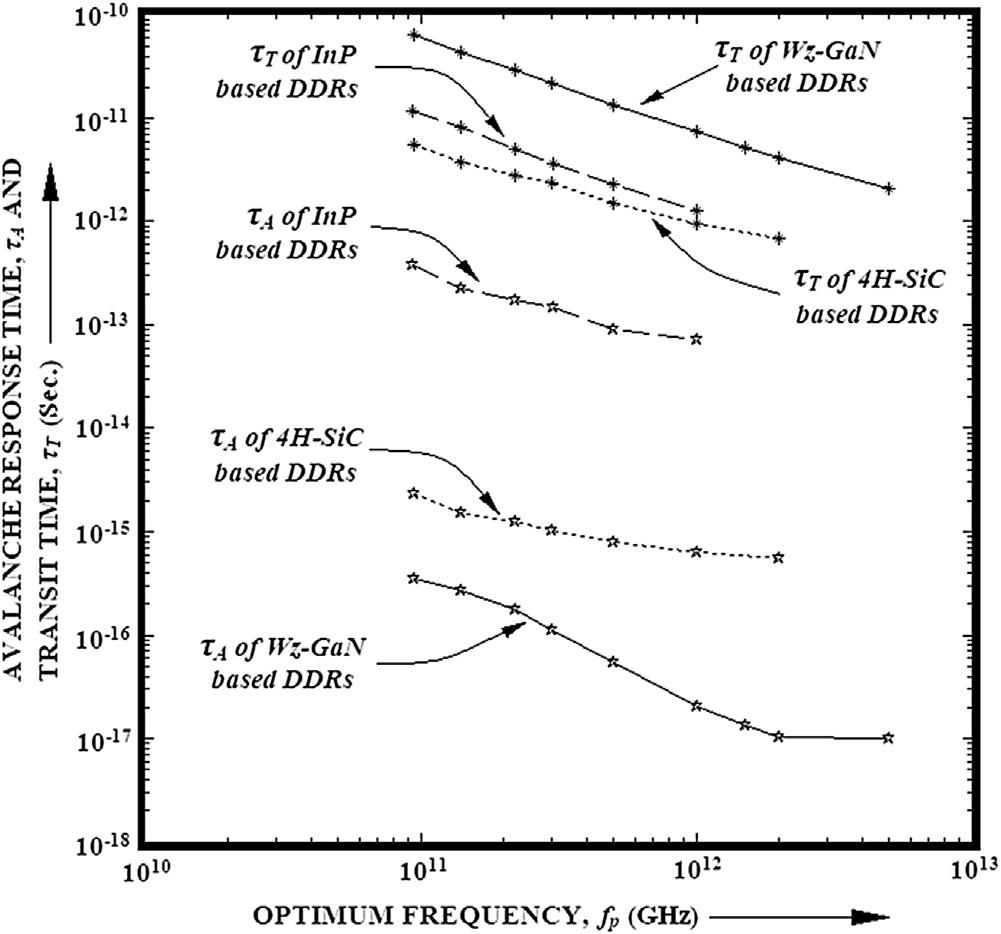
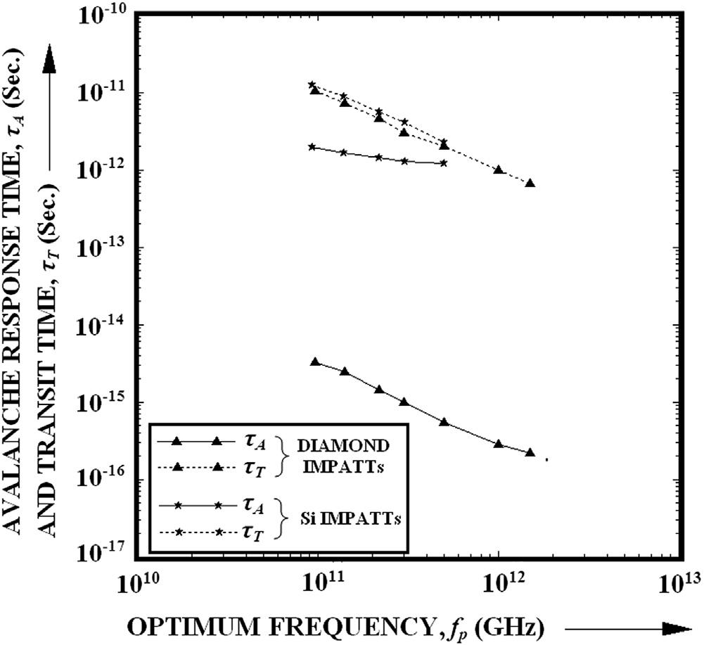
Figs.1.5and1.6 showthevariationsof sA and sT withoptimumfrequencyforDDRIMPATTdiodes madeofconventional(Si,GaAs)andWBG(4H-SiC, WZ-GaN,InP),semiconductorsrespectively.Within theoperatingfrequencyrange,ARTislessthanTTin DDRIMPATTdiodesandthiscanbedeterminedfor differentbasesemiconductingmaterialsfrom Figs.1.5 and1.6.ART(sA)dependsontwoimportantmaterial parametersviz.saturateddriftvelocityandionization rateofelectronsandholes(vsn, vsp and an, ap)inthe basesemiconductorofIMPATTdevice.Thus, sA isa functionofbasematerial.
Itisobservedfrom Fig.1.5 thatART(sA)inDDR GaAsIMPATTsislongerthanthatinDDRSidevice byfactorsof1.47and2.15atfrequenciesof94and 220GHz,respectively.Thecut-offfrequenciesof double-driftIMPATTsbasedonSiandGaAsareestimatedas500and220GHz,respectively,bydeterminingthefrequencyabovewhichARTexceedsTT from Fig.1.5.
Whenavalancheprocessisinitiatedbyamixtureof electronsandholes,thenthecorrespondingresponse time sA isgivenby
wheretheparameter k ¼ Jps/Js and(1 k) ¼ Jns/Js.
In Eq.(1.4), Jns and Jps arethereversesaturationcurrentcomponentsofthermallygeneratedelectronsand holes,respectively,and Js ¼ Jps þ Jns isthetotalreverse saturationcurrent.TheARTscanbecalculatedusing Eqs.(1.2) (1.4) bytakingtherealisticmaterialparametersfromRef.[46 49].
Itisobservedfrom Fig.1.6 thattheARTs, s A ofboth Wz-GaNand4H-SiCDDRIMPATTs,areordersof magnitudeshorterthanofDDRInPdevices.For example,at94GHz, s A ofWz-GaNand4H-SiCDDR IMPATTsare9.18 10 4 and6.26 10 3 timesof s A ofInPDDRIMPATTs,respectively.At1.0THz,the abovefactorsare2.82 10 4 and8.58 10 3 ,respectively.DDRIMPATTdiodebasedonGaNhasthe shortest s A ascomparedwithDDRdevicesbasedon 4H-Sic,InP,Si,andGaAs. Fig.1.6 showsfurtherthat GaNDDRIMPATTdevicecanoperateuptoa frequencyof5.0THzatsinceitsARTisoftheorder of10 16 sanditsTTisapproximately5ordersof magnitudelonger.TheresultsindicatethatSi-and GaAs-basedDDRdevic escandeliversigni fi cantRF powerat0.22and0.50THz,respectively,whilethose basedon4H-SiCandInPcandeliverpoweratmuch higherfrequencyof1THz.
AVALANCHE RESPONSE TIME, A AND TRANSIT TIME, T (Sec.) τ τ
A of G As based DDRs τ α T of G As based DDRs τ α
A of Si based DDRs τ T of Si based DDRs τ
OPTIMUM FREQUENCY, fp (GHZ)
FIG.1.5 Plotsofavalancheresponsetimeandtransittimeagainstoperatingoptimumfrequencyofdoubledriftregion(DDR)IMPATTsmadeofSiandGaAs.
FIG.1.6 Plotsofavalancheresponsetimeandtransittimeagainstoperatingoptimumfrequencyofdoubledriftregion(DDR)IMPATTsbasedonGaN,InP,and4H-SiC.
ARTAnalysistoDeterminetheOptimum OperatingFrequenciesofSi-andDiamondBasedDDRIMPATTDevices
Eq.(1.4) isusedtocalculateART(sA)ofbothSi-and diamond-basedDDRdevicesatdifferentoperatingoptimumfrequencies.Theelectronandholeionizationrates (an, ap)dependstronglyonelectric field(E)andhence onthespatialcoordinate(x)intheactivelayerofthedevice.Thus, an (x)and ap (x)in Eq.(1.4) canbeobtained
oncetheelectric fieldprofileintheactiveregionofthe deviceissimulated.The fieldprofileisobtainedthrough simultaneousnumericalsolutionoffundamentaldevice equationssubjecttoappropriateboundaryconditionsat depletionlayeredges.ThecarrierTTsinthedriftlayersof DDRdevicesatdifferentoperatingfrequenciesarecalculatedusingthesimplifiedformulareportedinRef.[50].
Fig.1.7 showstheplotsof sA and sT fordiamondand SiDDRIMPATTsversusoptimumfrequency.Abovea
FIG.1.7 Plotsofavalanchetransittimeandtransittimeversusoptimumfrequencyofdiamond-andSi-based IMPATTs.
certainhighfrequency,thecarriertransittime(sT) becomesshorterthantheART(sA)duetowhichthe RFperformanceofthedevicebecomeslimited[7,44].
Itisquiteevidentfrom Eq.(1.4) that sT dependson theterms an (x)and ap (x).Thus,theART, sA ata fixed operatingfrequencyisverymuchdependentonthe basesemiconductormaterial. Fig.1.7 showsthat sA of SiDDRdeviceat94GHzis5.99 102 timeshigher thanthatofdiamondDDRdevice,whereasat 0.5THz, sA ofSiDDRis2.21 103 timeshigherthan sA ofdiamondDDR.Theresultsclearlyindicatethat comparedwithSiDDRIMPATTs,diamond-based IMPATTscanbeoperatedforpowergenerationat higherfrequencyof1.5THz.Above1THz,ART(sA) ofdiamondIMPATTsisintherangeoffemtosecond (1.0 0.1 10 15 s),about4ordersshorterthanthat ofSidevices.ARTanalysiscarriedoutforSiDDR devicesshowsthattheirRFperformanceisavalanche responselimitedabove0.5THzfrequency.
ANOVERVIEWOFDESIGN,SIMULATION, ANDANALYSISOFIMPATTS
Ageneralizeddouble-iterative fieldmaximum computermethodfreefromanysimplifyingassumptionwasproposedbyRoyetal.[51]in1979tostudy theDCpropertiesofIMPATTsofanyarbitrarydoping profile.Thismethodprovideselectric fieldprofi le,
currentdensityprofile,avalancheregionwidth,voltage dropsacrosstheavalancheanddriftzones,breakdown voltage,andef ficiencyofDCtoRFconversion.SmallsignalanalysisandsimulationofIMPATTswaslater reportedbyRoyetal.[52].Thisanalysistakesinto accounttheeffectofmobilespacechargeandrealistic field-dependentionizationratesanddriftvelocitiesof chargecarriers.Thesmall-signaladmittancecharacteristics,negativeresistivity,andreactivityprofilesofthe devicewereobtainedfromthesmall-signalsimulation basedonGummel-Blueapproach.Banerjeeetal.in 1991[53]studiedthesmall-signalpropertiesandRF performanceofsimple flatandcomplexlow-high-low dopingprofilesofDDRSiIMPATTsatV-bandbycarryingoutsmall-signalsimulation.Thedesignresults wereusedtofabricatethedevicesbysiliconmolecular beamepitaxy.Acloseagreementbetweentheoretical andexperimentalresultsshowedtheaccuracyofthe method.
Theeffectoftemperatureonthesmall-signaladmittancecharacteristicsofIMPATTdiodewasstudiedby Y.Takayama[ 54 ]in1975.Hirachietal.[ 55 ]fabricated SiIMPATTdeviceforoperationatmm-wavefrequency andshowedthattheDCtoRFconversionef fi ciencyof thedevicecanbeimprovediftheohmiccontactofthe deviceismadewiththehelpofion-implantedtechnique.Theeffectofcarrierdiffusiononthestaticand microwaveperformanceofIMPATTdiodewasstudied
theoreticallybyM.S.Gupta[56 ].Theeffectof tunnelingonthehigh-frequencyperformanceof IMPATTdiodewasstudiedbyChiveetal.[ 57].Some reportsareavailableontheexperimentalrealization ofIMPATTdevices.K.B.Winterbon[ 58 ]fabricated IMPATTdevicebyion-implantationtechniqueand reportedtherangeofionbeamenergyusedintheprocess.Thehigh-frequencylimitationofsiliconIMPATT diodeswasstudiedbyDoumitriaetal.[59 ].Wanetal. [ 60]in1975reportedamultilayerepitaxialgrowth processforfabricationofsiliconIMPATTdiodeat mm-wavefrequencies.
DesignofStructuralandDopingParameters
TheoperatingfrequencyofDDRIMPATTdiode dependsonthetransittime(sT)ofchargecarriersto crossthedepletionlayerofthedevice.Thestructural anddopingparametersofthedevicedependonthe designfrequency( fd).Thefollowingsimpledesignformula[50]isusedtoobtainthedepletionlayerwidths ofnandpregionsofthedevice:
Wn;p ¼ 0:37vsn;sp =fd (1.5)
where vsn,sp arethesaturationvelocitiesofelectronsand holes,respectively.Thebackgrounddopingconcentrationsof n- and p-depletionregions(ND, NA)areinitially chosenaccordingtothedesignfrequency.Thedoping concentrationof nþ - and pþ-layersarenormallytaken tobesame,i.e., Nnþ ¼ Npþ ¼ 1026 m 3.TheseparametersareusedasinputdataforDCsimulation.Theelectric fieldprofileinthedepletionlayerandtherespective punchthroughfactorcanbeobtained.Thedopingparametersandthedopingprofilearesuitablyadjusted sothattheelectric fieldjustpunchesthroughthedepletionlayerofthedeviceataparticulardesignfrequency, fd,andaparticularbiascurrentdensity(J0).Small-signal simulationiscarriedouttoobtaintheadmittance characteristicsofthedevice.Varioususefulinformation ontheRFpropertiesofIMPATToscillatorsuchas optimumfrequency( fp),avalancheresonancefrequency,Q-factor,andbandwidthcanbeextracted fromtheadmittanceplots.
Theoptimumfrequency f p isthatfrequencyat whichthenegativeconductanceofIMPATTsreaches apeakunderoscillatingcondition.Thisfrequency canbeobtainedfromtheadmittance(conductancesusceptance)plotsofthedevice.Thedesignshould takecareofbringingthevalueof f p closertothedesign frequency, f d.Thiscanbedonebyadjustingthebias currentwithintheoperatingrange.Thebiascurrent densityisthen fi xedforaparticulardesignfrequency. Thesimulationisdonebytakingrealisticdoping
pro fi leofDDRIMPATTsusingappropriatedoping functionsindifferentregionsofthedevice.Thedesign parametersofthedevicemadeofdifferentsemiconductors,obtainedfromtheaforementionedmethod, aregivenin Table1.1 .Variousmaterialparameters suchas fi eld-dependentionizationrates(a n , a p),drift velocities( vn , vp)ofchargecarriers,bandgap( Eg ), intrinsiccarrierconcentration(n i ),effectivedensity ofstatesofconductionandvalencebands(Nc , N v), diffusioncoef fi cients(D n, Dp),mobilities(m n , m p), anddiffusionlengths(L n, Lp)ofthesemiconductors canbeobtainedfromRefs.[48 ,61 63 ].Thejunction diameterofIMPATTdeviceataparticularfrequency ( Dj)canbeobtainedfromarigorousthermalanalysis consideringappropriateheatsinkarrangement.The report[ 64 ,65]showsthatthevalueof Dj is35 mm forCWoperationofSiDDRIMPATTsat94GHz.
SomereportsontheDCpropertiesofIMPATT diode
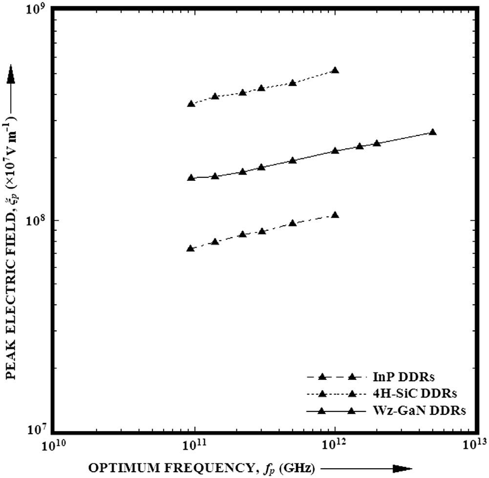
TheimportantDCparametersofthedevicecanbe obtainedfrommodelingandsimulationprogram describedinRefs.[ 51 ].Theseparametersare(i)peak electric fi eldatthemetallurgicaljunction(x P), (ii)breakdownvoltage( V B),(iii)voltageacrossthe avalanchelayer( VA ),(iv)ef fi ciencyofDCtomicrowaveconversion(h ),(v)widthofavalanchezone ( xA ),and(vi)fractionalvalueofavalanchezonewidth withrespecttototalwidthofactivelayer(xA/ W). Table1.2 showstheaforementionedDCparameters. Thevariationsof xP , V B,and h withoperatingfrequencyareshownin Figs.1.8 1.10 forDDRIMPATTs basedonSi,GaAs,InP,Wz-,and4H-SiC.ThesimulatedDCparametersofthedevicemadeofdifferent materialscanbecomparedbyusing Table1.2 and Figs.1.8 1.10 atdifferentoperatingfrequencies.Itis observedthatthepeak fi eld( xP)atthep-njunction ofDDRIMPATTsincreaseswithincreasingfrequency ( Table1.2 ). Table1.2 showsthatwithincreasingfrequency,thereversevoltageatbreakdown(V B ),width ofavalanchelayer( xA ),andvoltagedropacrossthe avalanchezone(V A )ofthedevicedecrease.Itisalso observedfromthetablethatwithincreasingfrequency,theDCtoRFconversionef fi ciency( h )of DDRIMPATTsbasedondifferentsemiconductorsdecreases.TheDCpropertiesofIMPATTsdependvery muchonthematerialpropertiesandthereforevary withthechangeofbasematerialofIMPATTs.Ata particularoperatingfrequency,thepeakelectric fi eld ( xP )in4H-SiCDDRsisfoundtohighestascompared withDDRsbasedonothermaterials.Thepeakelectric fi eld, xP,inGaNDDRIMPATTsisofthesameorderas thatin4H-SiCDDRs,butitsmagnitudeinDDR
DesignParametersofDouble-DriftRegionIMPATTsatmm-WaveandTHzFrequencies.
Semiconductor
Wz-GaN941.0501.58001.58000.5900.6005.0002.70035.00 1402.2501.05001.05000.6900.7105.0002.70025.00 2204.2750.73500.73501.0501.1005.0002.70020.00 3008.7000.53500.53501.5501.6005.0002.70015.00 50018.3750.33000.33002.8602.9005.0002.70010.00 100045.0000.18500.18506.8407.2005.0002.7005.00 150055.5000.13000.13009.80010.505.0002.7002.50 200072.0000.10200.102013.50014.5005.0002.7001.20 500088.5000.05200.052035.50036.5005.0002.7000.70 InP944.5000.32000.32001.9001.9005.0002.70035.00 1407.7000.21000.21003.4003.4005.0002.70025.00 22012.0000.13000.13005.2005.2005.0002.70020.00 30020.0000.10000.10107.2007.2005.0002.70015.00 50047.0000.06500.065013.50013.5005.0002.70010.00 100060.0000.02850.028528.00028.0005.0002.7005.00
Type-IIbdiamond (C) 944.0000.78000.72000.4600.5305.0002.70035.00 1407.5000.53000.53000.8100.8705.0002.70025.00 22013.0000.32000.32001.3501.4905.0002.70020.00 30017.0000.22000.22002.0502.2205.0002.70015.00 50025.0000.12000.12003.7504.1005.0002.70010.00 100039.0000.05200.05209.50010.0005.0002.7005.00 150048.0000.03000.030036.00037.0005.0002.7002.50
4H-SiC942.1000.58000.58002.8002.9005.0002.70035.00 1404.3000.40000.40004.9005.0005.0002.70025.00 2209.3000.30000.30006.9007.0005.0002.70020.00 30016.6000.25000.25009.50010.5005.0002.70015.00 50060.0000.16000.160014.50016.5005.0002.70010.00 1000210.0000.09000.090037.00043.0005.0002.7005.00
Si943.4000.40000.38001.2001.2505.0002.70035.00
1405.8000.28000.24501.8002.1005.0002.70025.00 22014.5000.18000.16003.9504.5905.0002.70020.00 30024.5000.13200.11206.0007.3005.0002.70015.00 50055.0000.07200.072015.00016.2005.0002.70010.00
GaAs12.205.606728.8717.0613.02376.040.00 25.606.044222.6715.579.97332.055.33 311.507.306715.7811.418.82208.054.74 424.509.131711.619.495.77146.066.36
Si13.406.011524.2716.2110.58352.046.32 25.806.661718.9813.529.16268.053.07 313.08.199013.7410.297.99170.053.10 417.29.349011.299.076.25134.059.82 552.012.17609.067.754.5990.067.16
InP11.407.390428.8214.4215.90230.033.72 22.907.927919.7810.4415.02156.033.91 35.008.590413.307.4813.93104.037.01 47.808.920510.716.2913.1384.041.79 519.09.74477.084.5611.3556.046.67 640.510.64504.433.347.8238.067.85 4H-SiC14.0035.9060226.08111.0916.19382.033.81
31.0017.0345155.1381.5715.49560.039.16 41.5017.8712118.1362.2115.07408.038.49 53.0019.276576.3441.4214.56252.039.38 610.821.473941.7624.2813.32134.040.61 716.022.476631.4319.3112.27102.045.95 823.523.377825.2116.1311.4682.048.81 930.026.381211.929.725.8844.067.69
IMPATTsbasedonInP,Si,andGaAsisoneorderlower inDDRsbasedonWBGsemiconductorssuchasGaN andSiC.Themagnitudeofelectric fi eld, xP ,atthe metallurgicaljunctionofDDRInPIMPATTdeviceis highestandthatofDDRGaAsdeviceislowest.In thiscontext,itisworthwhiletonotethatthemagnitudeofpeak fi eld x P increaseswiththeincreasingfrequency( Table1.2 ).Itisobservedthat x P in4H-SiC DDRIMPATTsincreasesfrom3.59 10 8 at94GHz to5.17 10 8 Vm 1 at1.0THz.
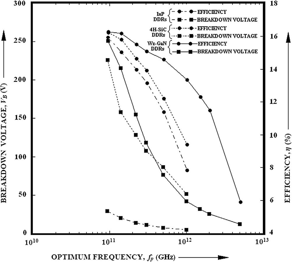
Itisobservedfrom Table1.2 thatthereversevoltage atbreakdown(VB)ishighestinDDRGaNdevices amongallotherDDRdevices.Thebreakdownvoltages ofDDRsbasedonWBGsemiconductorslike4H-SiC andWz-GaNarefound(Table1.2, Figs.1.8and1.10) tobelargerthanthosebasedonconventional
Thedifferenceofbreakdownvoltage(VB)and avalanchezonevoltage(VA)ofDDRdeviceisthe voltagedropacrossitsdriftzone,i.e., VD ¼ VB VA. AccordingtoScharfetter-Gummelsemiquantitativeformula[66],theDCtoRFconversionefficiencyof IMPATTdeviceisgivenby h ¼ (2m/p) (VD/VB)where thevoltagemodulationfactor,m,istakentobe0.5. Therefore, h ¼ (1/p) (VD/VB).Thismeansthathigher theratio(VD/VB),higheristheefficiencyofDCtoRF conversion. Figs.1.8and1.10 showthatwithincreasing frequency,theconversionefficiencydecreasesforall DDRdevicesduetothedecreaseoftheratio, VD/VB TABLE1.2
semiconductorslikeSi,GaAs,andInP.BetweenSiand InPDDRIMPATTsoperatingatthesamefrequency, thereversebreakdownoccursathighervoltage(VB)in InPDDRdevices(Table1.2, Figs.1.8and1.10).
FREQUENCY, fP (GHz)
FIG.1.8 Plotsof h, VB,and xP ofdouble-driftregion(DDR)SiandGaAsIMPATTsversusoptimumfrequency.
FIG.1.9 Plotsofpeakjunction field xP ofdouble-driftregion(DDR)IMPATTsbasedonInP,4H-SiC,andWzGaNagainstoptimumfrequency.
Fig.1.10 showsthatat94GHz,theefficiencyversusfrequencycurvesofdouble-driftIMPATTsbasedon4HSiCandWz-GaNintersecteachother.Thismeansthat 4H-SiCandGaNDDRdeviceswillhavesameefficiency at94GHzfrequency.However,at1THz,4H-SiCDDR IMPATTswillhavemuchlowerefficiencythanGaN DDRdevices.TheDCtomicrowaveconversion
efficiencyishighestinInPDDRIMPATTsfollowedby SiandGaAsDDRdevices(Figs.1.8and1.10).
TheRFperformanceofSiandGaAsDDRdevices withrespecttotheiref fi ciency(h )canbecompared atdifferentfrequenciesintherangeof94 500GHz from Fig.1.8 .Itisobservedthattheef fi ciencyofSi DDRsishigherthanGaAsDDRswithinthefrequency
FIG.1.10 Plotsof VB and h versusoptimumfrequencyfordouble-driftregion(DDR)IMPATTdevicesbased onInP,4H-SiC,andWz-GaN.
rangeof150 220GHz.At140GHz,theef fi cienciesof SiandGaAsDDRsarenearlythesame.Itisobserved from Fig.1.10 thatDDRsbasedonWBGsemiconductorslikeWz-GaNand4H-SiCshouldprovidehigher ef fi ciencythanthosemadeofconventionalsemiconductorslikeSiandGaAs(Fig.1.8 and Table1.2 ).The aforementionedresultsclearlyindicatethatGaN DDRdevicesexcelallotherDDRswithrespectto achievinghighef fi ciencyintheTHzfrequencyband. Itisinterestingtonotethattherateofdecreaseof ef fi ciencywithincreasingfrequency( d h /df )islower inGaNDDRsthanthatin4H-SiCandInPDDRsup toamaximumfrequencyof1THz.Thus,GaNDDRs haveanedgeoverotherDDRsasregardhigh-power deliveryandhighconversionef fi ciencyintheTHz frequencyband.
Table1.2 showsthattheratioofavalanchezone widthtototaldriftlayerwidth(xA/W)increasesfor eachbasematerialofDDRIMPATTsasonemoves fromserialnumber1tohigherserialnumberwhich correspondstoincreasingfrequency(Table1.3).This indicatesthattheavalanchezonewidenswith increasingfrequency.Thus,thevoltageacrossthe avalanchezone(VA)increasesandconsequentlythe voltageacrossthedriftzone(VD)decreaseswith increasingfrequency.Theratio VD/VB decreasesand correspondinglytheconversionefficiency(h)decreases withincreasingfrequency.Theratio xA/W ofGaASDDR IMPATTsincreasesfrom40.0%to66.36%asfrequency increasesfrom60to220GHzandtheDCtoRFconversionefficiency h decreasestoalowvalueof5.77%in GaAsDDRIMPATTsat220GHz.Similarly,incaseof SiDDRIMPATTs, xA/W increasesfrom53.10%to 67.16%and h decreasesfrom7.99%to4.55%asthe frequencyincreasesfrom220to500GHz(Table1.2). Itisfurtherobservedthat xA/W ofDDRsbasedon InP,4H-SiC,andWz-GaNincreasesfrom41.79%to 67.85%,37.08%to61.33%,and38.49%to40.61%, respectively,asfrequencyincreasesfrom300GHzto 1THz.Itisinterestingtonotethatintherangeoffrequency0.3 1THz, xA/W ofGaNDDRsremainsalmost constantwithoutappreciableincreaseincontrastwith thatof4H-SiCandInPDDRs(videserialnumbers 4,5,6of Tables1.2and1.3).But xA/W ofGaNdevices increasesappreciablyabove1THz.Withtheincreaseof frequencyfrom1 5THz, xA/W ofGaNDDRIMPATTs increasessharplyfrom40.61%to67.69%(column9, serialnumbers6 9of Tables1.2and1.3).Thisincrease of xA/W causesincreaseofVA/VB anddecreaseofVD/VB, leadingtosharpdecreaseofconversionefficiencyfrom 13.32%to5.88%(column7,serialnumbers6 9, Tables1.2and1.3).Similarlytheconversionefficiency of4H-SiCDDRdevicedecreasesfrom13.13%to7.82% andthatofInPDDRsdecreasesfrom13.89%to9.38% withincreaseoffrequencyfrom0.3to1THz.Allthe aforementionedDCresultsindicatethatGaNDDR IMPATTscanemergeasusefulsourcesofpowergenerationintheTHzfrequencyregime.
2.95483.52931.19 13.94611828.4755.0
5.88867.86621.34 6.0988909.8935.0
2.1438400.0425.0
17.145256.79703.31 0.4871226.8920.0 Si194 4.00026.56541.64 6.7679708.4335.0 2140 8.077215.46971.92 2.6524446.3525.0 3219 18.033438.78852.15 0.9855334.2320.0
High-frequencypropertiesofIMPATTdiode
High-frequencyparameterscanbeobtainedfrom small-signalsimulationofDDRIMPATTsmadeofconventionalandWBGsemiconductingmaterials. Table1.3 showstheseparameters,i.e.,optimumfrequency( fp), peaknegativeconductance(Gp),positivesusceptance (Bp),qualityfactoror Q-factor(Qp),negativeresistance (ZR),andRFpoweroutput(PRF)ofthedevices.
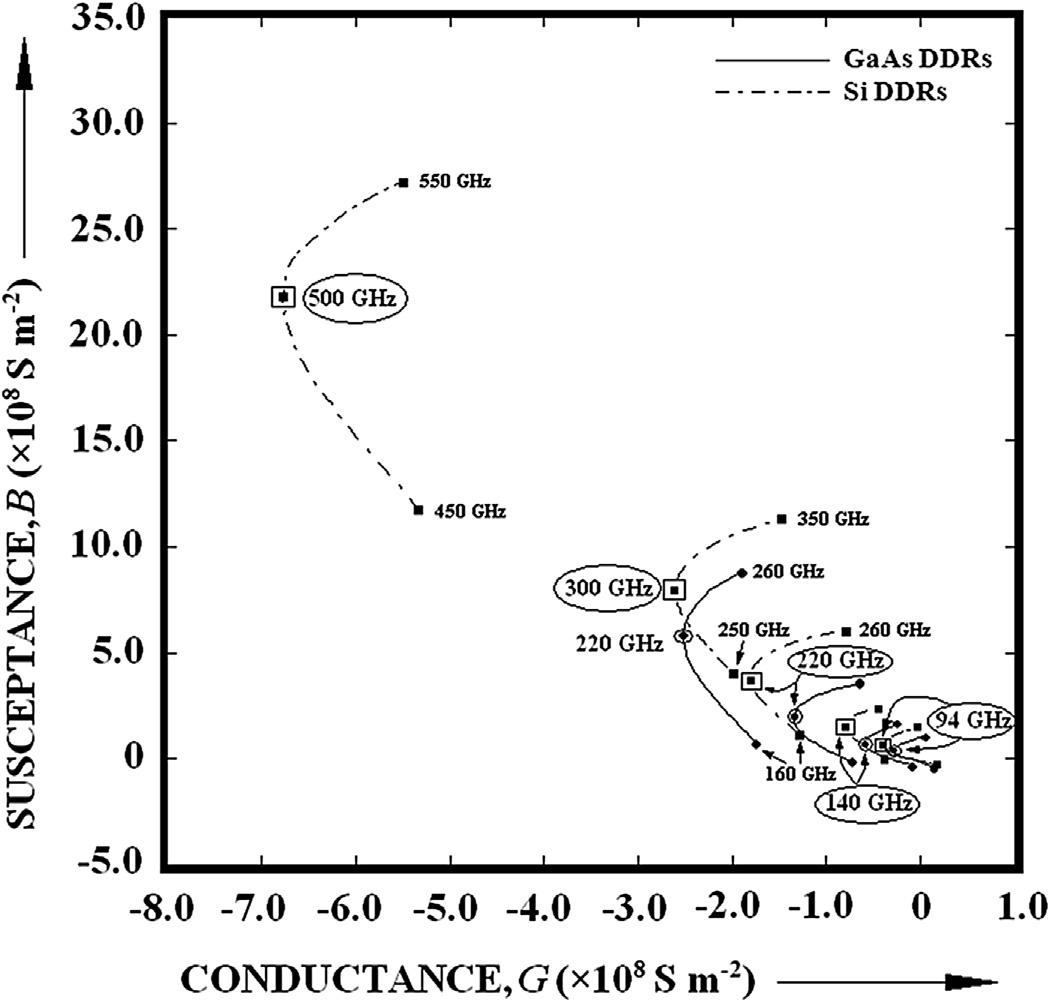
Fig.1.11 showsthesmall-signaladmittance,i.e., conductanceversussusceptance(G-B)plotsforGaAs andSiDDRIMPATTs.Theseplotsshowthatthe optimumfrequenciesforGaAsdevicesare94,140, 220,and300GHz,whilethoseforSidevicesare94, 140,220,300,and500GHz.Theadmittanceplots shownin Fig.1.11 clearlyindicatethatSiDDRIMPATTs canbeusedupto0.5THzincontrasttoGaAsIMPATTs.
0.1358504.165.0
0.0693192.092.5
0.036647.541.2
0.03457.620.7
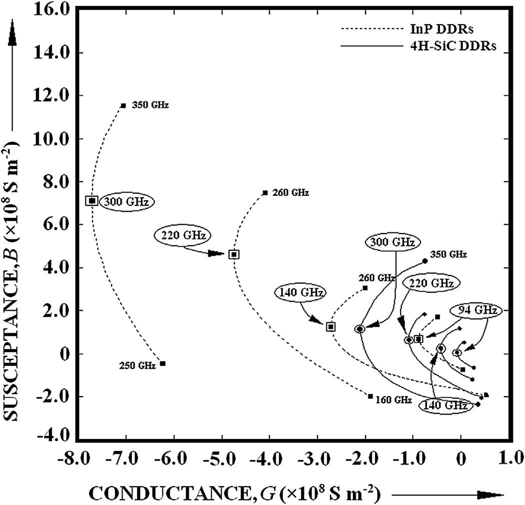
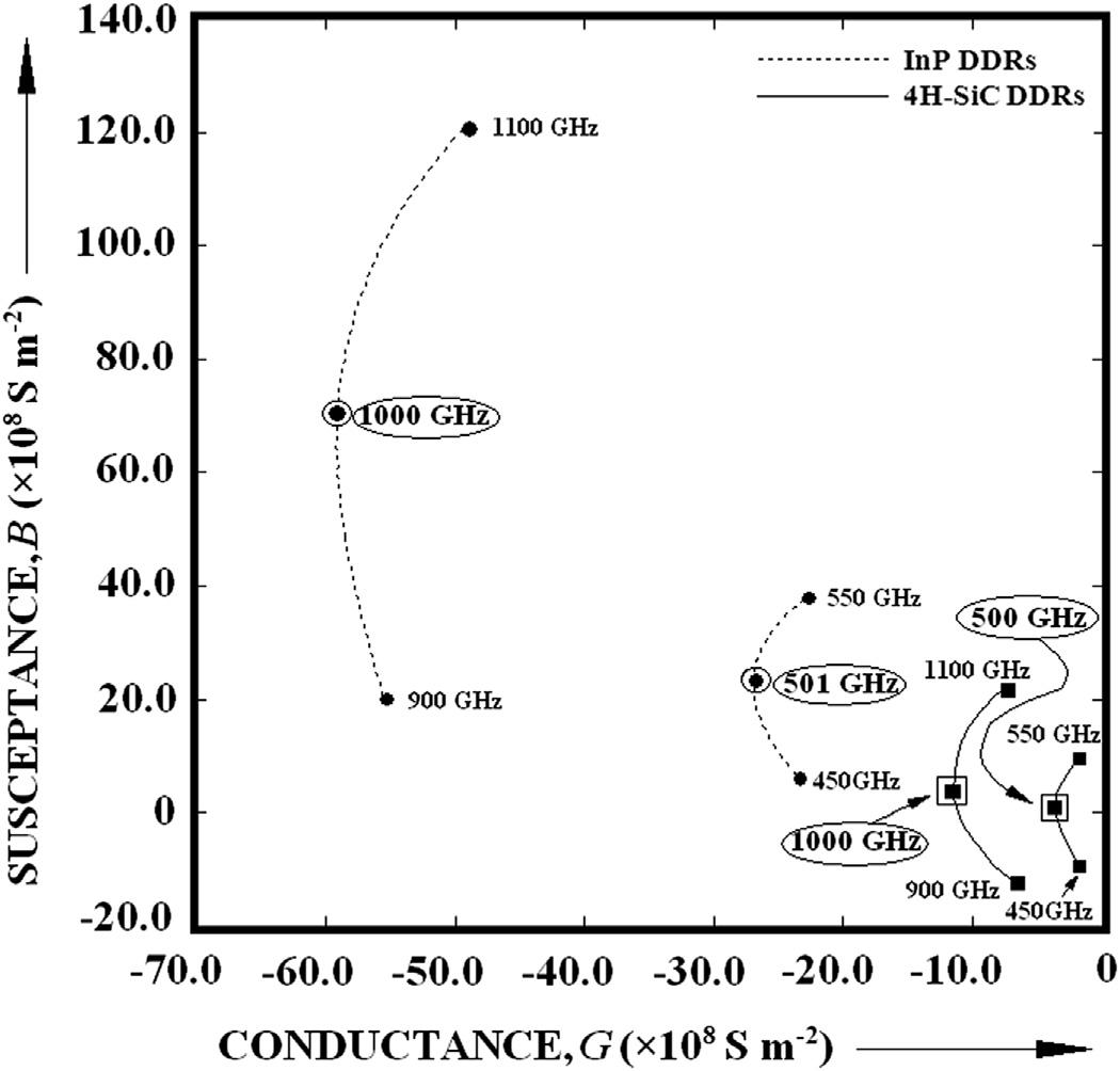
Figs.1.12 and 1.13 showtheadmittancecurvesofInP and4H-SiCDDRIMPATTs,respectively.Theoptimum frequenciesobtainedfromtheseplotsare94,140,220, 300,500,and1000GHzforbothInPand4-HSiC devices.
The Q-factor(Qp ¼ Bp/Gp)isanindicatorofconversionefficiencyandgrowthrateofoscillationin IMPATTdevices.Thisfactorshouldbeclosetoand slightlylessthan1(Qp z 1)toobtainstableoscillation andhigherefficiencyfromIMPATTdevices. Table1.3 showsthatthe Q-factorofInPDDRIMPATTsisthe lowestclosetounity(Table1.3)followedby4H-SiC DDRdeviceandothers. Table1.3 alsoshows Q-factorsofDDRIMPATTsbasedondifferentmaterials atmm-waveandTHzfrequencies.TheoptimumfrequenciesobtainedfromtheadmittanceplotsofDDR
FIG.1.11 Admittancecharacteristics(G-B)plotsofdouble-driftregion(DDR)IMPATTsmadeofGaAsand Si.
FIG.1.12 G-Bplotsfordouble-driftregion(DDR)IMPATTsbasedonInPand4H-SiC(optimumfrequencies areshown).
FIG.1.13 Admittance(G-B)plotsofdouble-driftregion(DDR)IMPATTdevicesmadeofInPand4H-SiC (optimumfrequenciesinTHzbandasmarked).
IMPATTsbasedonmediumandWBGsemiconductors playthedecisiveroletoselecttheproperbasematerial ofIMPATTsanddesignthesameforTHzoperation. Fig. 1.14 showstheadmittanceplotsofDDRIMPATTs basedonGaNattheoptimumfrequenciesof94,140, 220and300GHzwhichareincidentallythewindow frequenciesinthemillimeterwaveregion. Fig.1.15 showssimilarplotsattheoptimumfrequenciesof 500,1000,1500,2000and3000GHzie,0.5,1,1.5, 2.0and3.0THz.
Devicenegativeresistance(ZR)isanimportant parametertoestimatetheRFpoweroutputfromthe device. Table1.3 showsthesimulatedvaluesof ZR, obtainedfromtherealpartofdeviceimpedance.It decreaseswithincreasingfrequencyfordifferentbase materialsofDDRIMPATTsunderconsideration.Itis observedfrom Table1.3 that4H-SiCDDRIMPATTs exhibithighestnegativeresistance(ZR)amongallother DDRdevicesforthefrequencyrangeof94GHzto 1THz.Thehighestnegativeresistanceof4H-SiCDDR IMPATTsimpliesthatthesedevicesdeliverhighestRF powerattheoptimumfrequencyascomparedwith DDRdevicesbasedonothermaterials.
Fig.1.16 showsthevariationsofRFpoweroutput (PRF)withoptimumfrequencyforalltypesofDDR IMPATTs.Itisobservedthat PRF decreasesnonlinearly withincreasingfrequencyinallcases. Table1.3 gives
theoutputpowerfromIMPATTsbasedondifferent semiconductorsatdifferentoptimumfrequencies.Itis observedfromboth Fig.1.16 and Table1.3 thatSi DDRIMPATTsdeliverhigheroutputpowerthanGaAs IMPATTsat140and220GHzwindowfrequencies. Thecut-offfrequenciesabovewhichtheiritmaybe notedthattheRFperformancesofSiandGaAsDDRs arelimitedabove500and220GHz,respectively.These cut-offfrequenciesareobtainedfromavalanche responseanalysis.Thesimulatedoutputpowersfrom differentDDRdevicesareshownin Table1.3 and Fig.1.16.Asregardpowerdeliveryat94,140,and 220GHzwindowfrequencies,InPDDRsshouldbe preferredtoSiandGaAsDDRs.Moreover,InPIMPATTs arecapableofdeliveringpowerupto1THzfrequency. Theavalancheresponselimitstheoperatingfrequencies ofbothSiandGaAsDDRIMPATTsbelow1THz.Itis worthwhiletoobservefrom Fig.1.16 aswellas Table1.3 thatDDRIMPATTsbasedonWBGsemiconductorslike 4H-SiCandWz-GaNareexcellentcandidatesforTHz operation.Thereportedresultsindicatethatthese devicesarecapableofdeliveringhighpowerwithhigh conversionefficiencyatTHzfrequencies.Itmaybe concludedfromtheaforementionedresultsthat IMPATTdevicesbasedonWz-GaNarewithoutany competitionabove1THzasregarddeliveringhigh powerwithhighconversionefficiency.