Plasma Etching Processes for CMOS Device Realization
Edited by Nicolas Posseme
First published 2017 in Great Britain and the United States by ISTE Press Ltd and Elsevier Ltd
Apart from any fair dealing for the purposes of research or private study, or criticism or review, as permitted under the Copyright, Designs and Patents Act 1988, this publication may only be reproduced, stored or transmitted, in any form or by any means, with the prior permission in writing of the publishers, or in the case of reprographic reproduction in accordance with the terms and licenses issued by the CLA. Enquiries concerning reproduction outside these terms should be sent to the publishers at the undermentioned address:
ISTE Press Ltd
27-37 St George’s Road
Elsevier Ltd
The Boulevard, Langford Lane London SW19 4EU Kidlington, Oxford, OX5 1GB UK UK
www.iste.co.uk
www.elsevier.com
Notices
Knowledge and best practice in this field are constantly changing. As new research and experience broaden our understanding, changes in research methods, professional practices, or medical treatment may become necessary.
Practitioners and researchers must always rely on their own experience and knowledge in evaluating and using any information, methods, compounds, or experiments described herein. In using such information or methods they should be mindful of their own safety and the safety of others, including parties for whom they have a professional responsibility.
To the fullest extent of the law, neither the Publisher nor the authors, contributors, or editors, assume any liability for any injury and/or damage to persons or property as a matter of products liability, negligence or otherwise, or from any use or operation of any methods, products, instructions, or ideas contained in the material herein.
For information on all our publications visit our website at http://store.elsevier.com/
© ISTE Press Ltd 2017
The rights of Nicolas Posseme to be identified as the author of this work have been asserted by him in accordance with the Copyright, Designs and Patents Act 1988.
British Library Cataloguing-in-Publication Data
A CIP record for this book is available from the British Library Library of Congress Cataloging in Publication Data
A catalog record for this book is available from the Library of Congress
ISBN 978-1-78548-096-6
Printed and bound in the UK and US
2.2.4.
2.2.8.
2.3.
2.3.1.
Chapter 3.
Sébastien BARNOLA, Nicolas POSSEME, Stefan LANDIS and Maxime DARNON
3.1.
3.1.1.
3.1.2.
3.2.
3.3.
3.4.
Chapter 4.
Maxime DARNON and Nicolas POSSEME
4.1.
4.1.1.
4.2.
4.2.1.
4.2.2.
4.2.3.
4.3. Stopping
4.3.1. Foot/notch
4.3.2. Selectivity issues with thin SiO2 and silicon
4.3.3. Selectivity/residues with high-k
4.4. High-k
4.5. Line
4.6. Chamber wall
This page intentionally left blank
Preface
Plasma etching is the main technology used to pattern complex structures involving various materials (from metals to semiconductors and oxides to polymers) in domains such as microelectronics, bio-technology, photonics and microsensors. The ability of “cold plasmas”, including mainly inductively coupled plasmas (ICP) and capacitively coupled plasmas (CCP), to generate well-controlled etched profiles (anisotropic (vertical) etching) and high etch selectivities (selected material is etched at the much higher rate than others) between materials involved in complex stacks of materials has made this technology successful. The most famous field in which plasma technology has played a key role for the last 40 years is the semiconductor industry.
Plasma etching (using an ionized gas to carve tiny components on silicon wafers) has long enabled the perpetuation of Moore’s law (the observation that the number of transistors that can be squeezed into an integrated circuit doubles about every 2 years). Today, etch compensation helps to create devices that are smaller than 20 nm.
Plasma technologies have been critical not only to assist the miniaturization capabilities of lithography with specific processes such as resist trimming processes (lateral erosion of the photoresist mask in order to decrease its critical dimension defined by the lithography) and double patterning (a method of overlaying two patterns to achieve the original design) technologies, but also to pattern complex structures with the appropriate level of dimension control. However, with the constant scaling down in device dimensions and the emergence of planar fully depleted silicon on insulator (FDSOI) or complex 3D structures (like
FinFET sub-20 nm devices, nanowires and stacked nanowires at long term), plasma etching requirements have become more and more stringent with critical dimension control, profile control and film damage at the atomic scale to reach zero variability (precise control of the gate transistor dimension with no damage) required at the horizon of 2020 according to the ITRS.
Now more than ever, plasma etch technology is used to push the limits of semiconductor device fabrication into the nanoelectronics age. This will require improvements in plasma technology (plasma sources, chamber design, etc.), new chemistry methods (etch gases, flows, interactions with substrates, etc.) as well as a compatibility with new patterning techniques such as multiple patterning, EUV lithography, direct self-assembly (DSA), e-beam lithography or nanoimprint lithography.
The goal of this book is to present these etch challenges and associated solutions encountered through the years for transistor realization.
After an introduction to the evolution of CMOS devices through the years in Chapter 1, we will define in Chapter 2 the plasma etching in microelectronics. Then, in Chapter 3, we will present patterning challenges in microelectronics and how plasma etch technology becomes a key solution. Finally, in Chapter 4, we will present the challenges and constraints associated with transistor manufacturing.
Nicolas
POSSEME October 2016
CMOS Devices Through the Years
The CMOS transistor is the fundamental building block of modern electronic devices and is ubiquitous in modern electronic systems. Its dimension is typically around 20 nm and the unit cost of the device is around a few nano dollars.
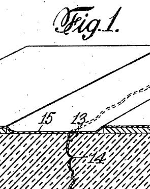
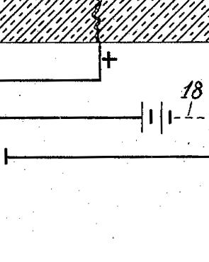
The basic principle of the solid state transistor was stated by Julius Edgar Lilienfeld in 1925 who patented “a method and apparatus for controlling the flow of an electric current between two terminals of an electrically conducting solid by establishing a third potential between said terminals” (Figure 1.1) [LIL 25].
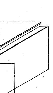
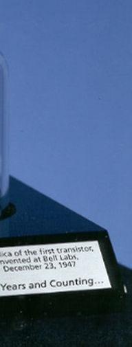
The experimental demonstration began in 1947 with American physicists John Bardeen, Walter Brattain and William Shockley who made the first point contact transistor (Figure 1.2). Working at Bell Labs, they were looking for a solution to replace the vacuum tubes which were not very reliable, consumed too much power and produced too much heat to be practical for AT&T’s markets. They were jointly awarded the Nobel Prize in Physics in 1956 for their achievement [NOB 47].
Chapter written by Maud VINET and Nicolas
POSSEME.
The the “po metal p
Fi pat
gure 1.1. Sch ented transist
Figure 1.2. by Bard first demons int contact” late. The cry
ematics of Lil or (from E.J. L
Artifact of the een, Shockley tration of a transistor m stal was co
ienfeld’s origin Lilienfeld [LIL
first point co and Brattain
ontact transisto n in 1947 in Be
semiconduc ade out of ntacted by
tor-based am a germanium a gold strip al 25])
r fabricated lls Labs plifying dev crystal lyi cut into tw ice was ing on a o pieces
which were a hair apart, and covered a triangle which was held in contact by a spring.
To improve the point contact transistor, Shockley conceived the possibility of minority carrier injection and invented an entirely new, considerably more robust, type of transistor with a layered or “sandwich” structure. This structure went on to be used for the vast majority of all transistors in the 1960s, and evolved into the bipolar junction transistor. At that time, though, the junction-based transistors were limited in performance, since they were not able to carry voice signals due to frequency limitations.
The man who paved the way for the improvement was Gordon Teal, who suspected that better grown materials of better quality could lead to better performance. Teal thought transistors should be built from a single crystal, as opposed to cutting a sliver from a larger ingot of many crystals. His method was to take a tiny seed crystal and dip it into the melted germanium then pull slowly as a crystal formed like an icicle below the seed.
In 1959, Dawon Kahng and Martin M. (John) Atalla at Bell Labs invented the metal–oxide–semiconductor field-effect transistor (MOSFET). Operationally and structurally, it was different from the bipolar junction transistor. The MOSFET was made by putting an insulating layer on the surface of the semiconductor and then placing a metallic gate electrode on that. It used crystalline silicon for the semiconductor and a thermally oxidized layer of silicon dioxide for the insulator. The silicon MOSFET did not generate localized electron traps at the interface between the silicon and its native oxide layer, and thus was inherently free from the trapping and scattering of carriers that had impeded the performance of the earlier field-effect transistors.
As the industry expanded, the fundamental fabrication operations (photolithography, etching, deposition and thermal treatment) became more and more specialized and intertwined. Relying on several suppliers, this specialization led the industry to advance at a fast pace. The need for a technology roadmap arose in order to coordinate the industry, so that each supplier could target an appropriate date for their part of the work [GAR 00].
For several years, the Semiconductor Industry Association (SIA) gave the responsibility of coordination to the United States, which led to the creation of an American style roadmap, called the National Technology Roadmap for Semiconductors (NTRS). The SIA produced its first technological roadmap in 1993.
In 1998, the SIA came closer to its European, Japanese, Korean and Taiwanese counterparts by creating the first global roadmap: the International Technology Roadmap for Semiconductors (ITRS). This international group has (as of the 2003 edition) 936 companies which were affiliated to working groups within the ITRS. These companies agreed upon the guidelines for device dimensions and specifications in order to provide guidance to the whole industry [ITR 13].
1.1. Scaling law by Dennard
Moore and Dennard’s ideas set the semiconductor industry on a course of developing new integrated circuit process technologies and products on a regular pace and providing consistent improvements in transistor density, performance and power.
Moore’s law states that each new generation of process technology was expected to reduce minimum feature size by approximately 0.7x. A 0.7x reduction in the linear features size was considered to be worthwhile for a new process generation as it translated to about a 2x increase in transistor density.
Dennard’s scaling law was the supporting physics guidance to preserve the CMOS operation while scaling its dimensions [DEN 74]. The scaling principles described by Dennard and his team were quickly adopted by the semiconductor industry as the roadmap for providing systematic and predictable transistor improvements.
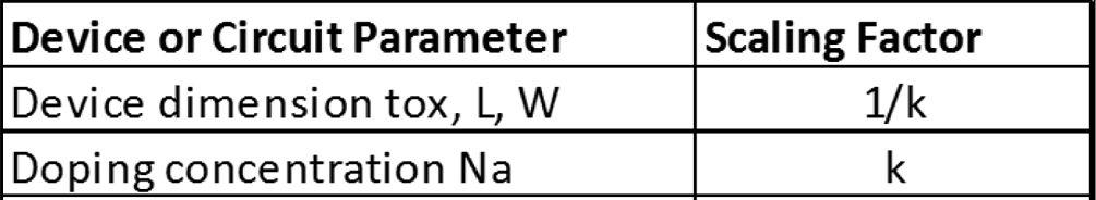
Table 1.1 is reproduced from Dennard’s paper and summarizes transistor or circuit parameter changes under ideal scaling conditions, where k is the unitless scaling constant [DEN 74].
Table 1.1. Scaling results for circuit performance (from B. Dennard et al. [DEN 74])
During the 1970s and 1980s, the semiconductor industry managed to maintain a fast pace and introduced new technology generations approximately every 3 years. This translated into a transistor density improvement of ~2x every 3 years, but this was also a period when average chip size was increasing, resulting in a transistor count increase of close to 2x every 18 months. Starting in the mid-1990s, the semiconductor industry accelerated the pace of introducing new technology generations once every 2 years. Today, the trend of increasing chip size has slowed down slightly due to cost constraints.
Historically, the transistor power reduction afforded by Dennard scaling allowed manufacturers to drastically raise clock frequencies from one generation to the next, without significantly increasing the overall circuit power consumption.
Since around 2005–2007, scaling faced a challenge that broke down Dennard’s scaling law. On reaching 100 nm (or the deep sub-micron channel length), maintaining the electrostatic integrity of the transistor became a major issue.
Some of the major problems to MOSFET scaling in sub-100 nm channel length regime were:
1) short channel effect (SCE);
2) drain induced barrier lowering (DIBL);
3) increased off-state current;
4) increased gate leakage;
5) poly gate depletion effects;
6) source/drain access resistance increase;
7) high-field mobility degradation;
8) variability.
In order to overcome these challenges, significant innovations were made at every new technological node.
1.2. CMOS device improvement through the years
The speed of high performance logic circuits depends on the drive current, which is the source–drain saturation current of the metal–oxide–semiconductor field-effect transistor (MOSFET). The improved performance of integrated circuits can be seen from the effect of the scaling on the drive current. Indeed, the saturation current Idsat of the MOSFET can be written as follows:
where W and L are the width and length of the MOSFET channel, μ is the channel carrier effective mobility, Cox is the gate oxide capacitance, VG is the gate voltage and VT is the threshold voltage.
Reduction of channel length L, increase of channel carrier effective mobility μ and gate oxide capacitance density Cox will result in an increased Idsat.
1.2.1. Mobility improvement
With the scaling of transistor dimensions, mobility in bulk devices suffered a severe degradation as higher doping levels were required to preserve the CMOS electrostatics. As a result, strain engineering was widely
accepted as a promising technique to overcome this mobility degradation and to restore CMOS performance to the 90 nm node.
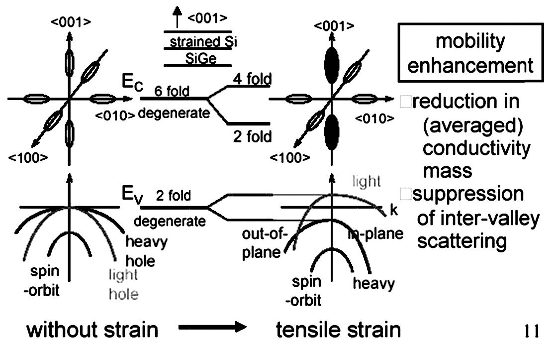
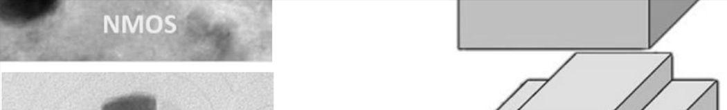
One key consideration in using strain engineering in CMOS technologies is that PMOS and NMOS respond differently to different types of strain. Specifically, PMOS performance is best served by applying compressive strain to the channel, whereas NMOS benefit from tensile strain (see Figure 1.3). Many approaches to strain engineering induce strain locally, allowing both n-channel and p-channel strain to be modulated independently.
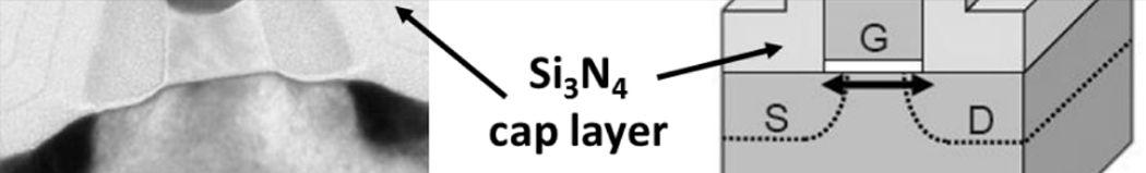
The first approach to be introduced involved the use of a strain-inducing capping layer. Chemical vapor deposition (CVD) silicon nitride was a common choice for a strained capping layer, in that the magnitude and type of strain (e.g. tensile vs. compressive) may be adjusted by modulating the deposition conditions, especially temperature. Standard lithography patterning techniques were used to selectively deposit either tensile or compressive strain-inducing capping layers on either N or PMOS.
Figure 1.3. NMOS band diagram with and without tensile strain. Tensile strain induces a degeneracy splitting in the <001> valleys. As a result, the electron concentration increases in the low effective mass subbands, resulting in a lowered averaged conductivity mass (from S-I. Takagi [TAK 03])
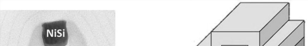
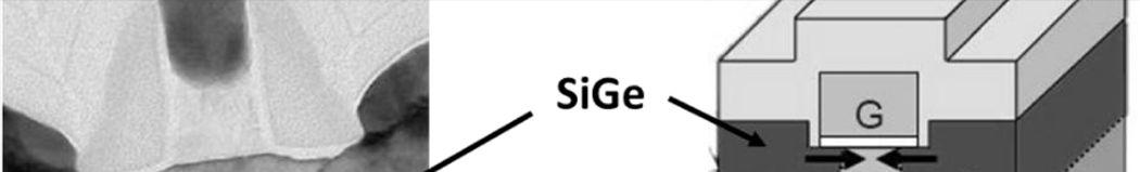
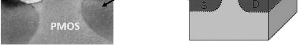
A second prominent approach in strain engineering involves the use of silicon-rich alloys, especially silicon-germanium, to modulate channel strain. For instance, compressive strain can be induced by replacing the source and drain region of a MOSFET with silicon-germanium (Figure 1.4).
Figure 1.4. Intel 65 nm technology corresponding to the second generation of uniaxial strained Si for enhanced performance (Lg = 35 nm, Tox = 1.2 nm) (adapted from S. Thompson [THO 05])
1.2.2. Leakage current reduction
The scaling of silicon dioxide dielectrics was an effective approach to enhance transistor performance in complementary metal–oxide–semiconductor (CMOS) technologies as predicted by Moore’s law (see equation [1.1]).
In the past few decades, a reduction in the thickness of silicon dioxide gate dielectrics has enabled increased numbers of transistors per chip with enhanced circuit functionality and performance at low costs. However, as the devices approach the sub-45 nm scale, the equivalent oxide thickness (EOT) of the traditional silicon dioxide dielectrics is required to be smaller than 1 nm, which is approximately 3 monolayers and close to the physical limit, resulting in high gate leakage currents due to the obvious quantum tunneling effect at this scale.
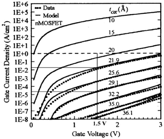
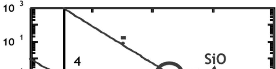
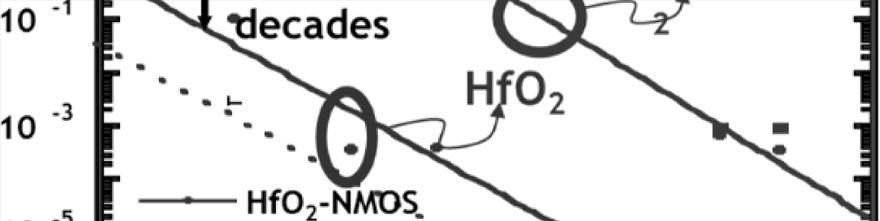
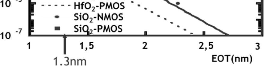
Figure 1.5 shows how gate leakage becomes the main contributor to leakage current when the equivalent oxide thickness was scaled down in the 1.5 nm range.
Figure 1.5. Gate leakage as a function of gate voltage for SiO2 gate oxide thicknesses ranging from 3.6 nm down to 1 nm. The threshold of 1 A/cm² was reached when gate oxide was below 2 nm for Vg = 1.5 V (from Y. Taur and E.J. Nowak [TAU 97])
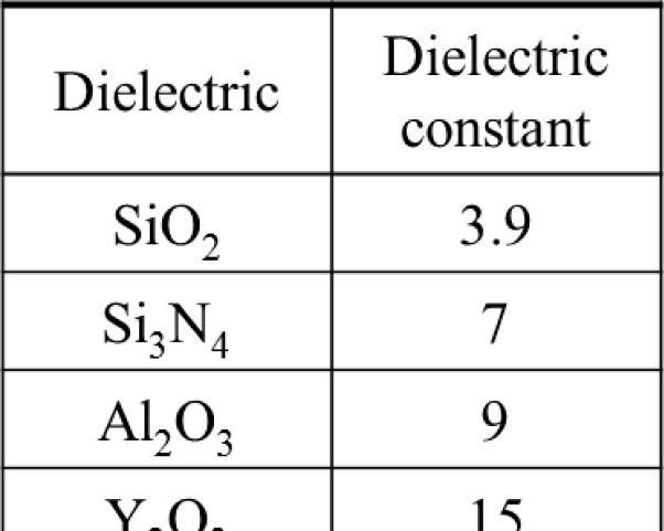
To continue the downscaling of the EOT, dielectrics with a higher dielectric constant (high-k) were suggested as a solution to achieve the same transistor performance and electrostatics, while maintaining a relative physical thickness.
Many candidates with a probable high-k gate dielectrics were considered to replace SiO2 (see Table 1.2).
Table 1.2. High-k gate dielectric candidates to replace SiO2
The industry first introduced oxynitride gate dielectrics in the 1990s, wherein a conventionally formed silicon oxide dielectric was infused with a small amount of nitrogen. The nitride content subtly raised the dielectric constant and allowed for a relaxed gate oxide thickness while maintaining good electrostatics.
To further contain the gate leakage, the gate oxide was afterwards replaced with high-k (high dielectric constant) dielectric material based on hafnium oxides (HfSiON and HfO2) and the gate leakage was divided by 4 decades, as illustrated in Figure 1.6. Intel was the first company to announce the deployment of high-k dielectrics in its 45 nm bulk technology.
Figure 1.6. Gate leakage as a function of gate voltage for SiO2 and HfO2 gate oxides. The effectiveness of HfO2 introduction is illustrated by a 4-decades reduction of the gate current at a given equivalent oxide thickness (EOT) as compared to SiO2 reference (from B. Guillaumot et al. [GUI 02])
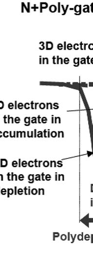
Together with the introduction of high-k dielectrics, metal gate stacks based on titanium nitride (TiN) replaced the doped polysilicon gate. A major challenge in the introduction of metal gate electrodes was the need to obtain distinct gate work functions for NMOS and PMOS devices. While two metals would ordinarily be required, a method was developed that allowed the metal gate work function to be tuned over the required range, based on Al and La diffusion in the gate dielectric.
The as illust thin equ F of t i 1.2.3. G
of metal ga re 1.7. Poly e thickness.
igure 1.7. Sch he example) p ncrease of th ate-last ap
ematics of th olysilicium ga e gate oxide t control of t proach
omitantly w on scheme w
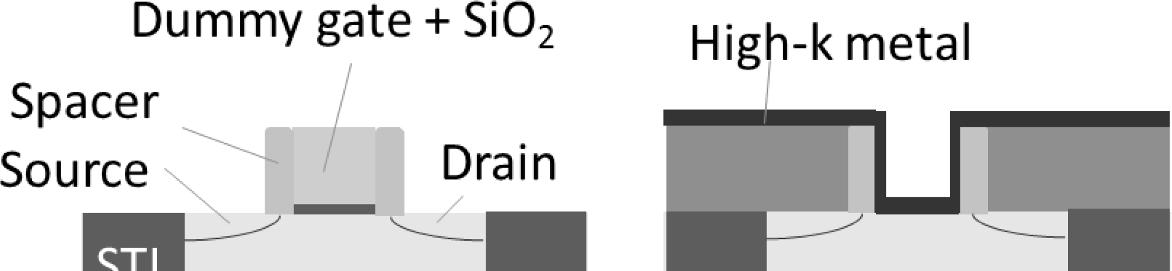
Indeed, the P etal undergo metal gate s also known scene proces mptied after re 1.8 repres gate patte on (Figure 1 ical mecha gate is selec high-k–wo gate (tungs ation step (F
Conc integrati PFETs. as the m Vt, the process, a Dama will be e Figu dummy realizati by chem dummy Finally, metal planariz introduction rated in Figu ivalent oxid
te stack sup depletion w e polydepletio te. This polyd hickness, resu he gate over t
ith the highas changed -type workes thermal b tack is depo as the replac s where a d RSD definit
ents a simpl rning using .8(a)), a sili nical polish tively remo rk-function ten) are d igure 1.8(f))
pressed the p as on the wa on effect in a N depletion resu ulting in a low he channel
Through the Y olydepletio y to benefiti + (for the sak lts in an appa er electrostati
e stack introd irst to gate-l ds to get mo Thus, in order unction acti l gate proces is used to d UI 02] for ear e of the gate entional ap film is depo 1.8(b)). In g a cavity in ) (Figure 1 Figure 1.8(e
k/metal gate from gate-f function ten udgeting. T sited after j ement meta ummy gate ion (see [GU ified scheme the conv con dioxide ing (Figure ved, creatin metal (TiN eposited (F . CMOS Devices
uction, the g ast to ensure re and more to target lo vation. The s (RMG), co efine a cavit ly work).
-last approac proach and sited and pl Figure 1.8 the silicon .8(d)) and )) followed
Years 11 on effect, ing from ke arent ic gate stack low Vt mid-gap ow PFET gate-last nsists of y which ch. After d spacer lanarized 8(c), the dioxide. capping d by a
1.2.4. New transistor generations
1.2.4.1. FinFET
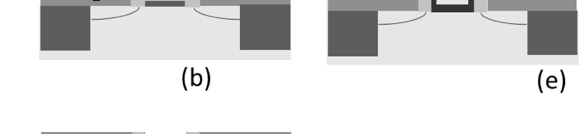
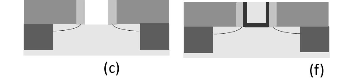
The most dramatic change in CMOS transistors was brought by Intel at 22 nm node, in the year 2011, with the introduction of FinFET architecture in production. FinFET devices belong to the fully depleted architectures (sometimes this statement can be argued depending on the junction isolation to the bulk substrate) like FDSOI, Gate-all-Around transistors and all the architectures where we can define a silicon thickness or width that is smaller than the depletion depth in the device. The architectures of the fully depleted family are shown in Figure 1.9.
The fully depleted architectures were introduced to restore the gate electrostatic control over the channel. Indeed when the gate length became shorter than 30 nm, it becomes extremely challenging for bulk planar devices to maintain low Ioff currents, in spite of very high channel doping and the use of halos (highly doped pockets at the entrance of the channel, of opposite channel type, designed in order to enhance the potential barrier at the source side).
Figure 1.8. Gate-last integration scheme
Figure 1.9. (a) Planar DG [BAL 87], (b) FinFET [HIS 89], (c) vertical surrounding gate [TAK 88], (d) gate all around (GAA) [COL 90], (e) thin film transistor on top of a buried oxide with a ground plane (from M. Fukuma [FUK 88])
Electrostatics in fully depleted architectures is controlled by the thin silicon film channel thickness or the Fin width. As shown in equation [1.2], the DIBL (and subthreshold slope) improves for a given gate length as a function of thinner silicon channel thickness or thinner Fin width as implemented in the Mastar model [SKO 93], which was the analytical model used to build ITRS specifications:
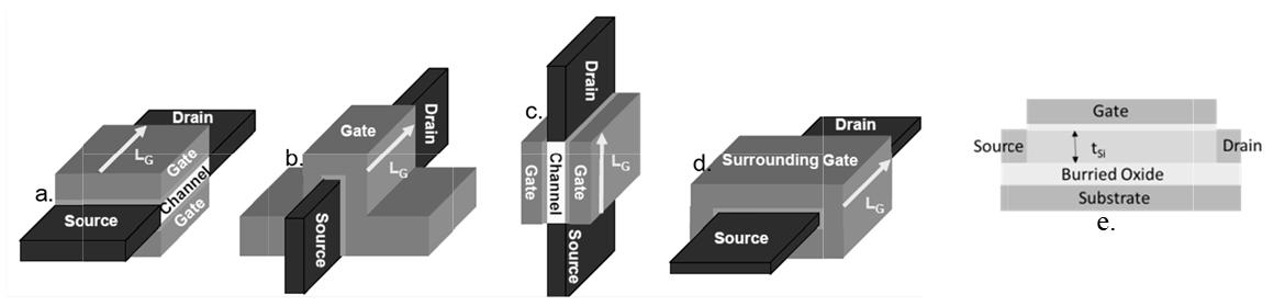
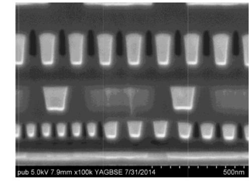
Figure 1.10 provides some SEM observations of Intel 22 nm FinFET. The fact that the active width is now discrete (a multiple of the number of Fin) appears clearly.
Figure 1.10. Left: top-down SEM observation of Intel 22 nm FinFET technology (from http://www.intel.com/content/www/us/en/silicon-innovations/intel-22nmtechnology.html). Middle: 14 nm Fin cross-section. Right: first metal levels cross-section (from S. Natarajan [NAT 14])
1.2.4.2
Anot recovery at 28 nm Si film decades benefits to lowe channel ultra-thi biasing multiple devices legacy b bulk tec CMOS to FDSO of 3 GH using 2 to reach further e
ma Etching for . Fully depl her answer was the in node. FDS (less than , FDSOI ha compared t r junction le to reduce th n BOX (aro for Vt tuni work-funct ; v) simple ulk IP prese hnology, all FEOL modu I [NGU 14 z [LEP 13, 8 nm node g mainstream xpanding w
CMOS Device
eted silicon from the troduction o OI is a plan 10 nm) on s been dem o the other o akage, capa reshold volt und 25 nm) ng and pow ion metal g co-integratio rvation; vi) owing for re les and sim ]. ARM-bas MAG 13] round rules manufactur ith foundry,
Figure 1.11. area. Beca FDSOI devi as compa
Vt matching a use of random ce, the variab red to the bulk Realization
on insulato semicondu f FDSOI tec ar technolo a buried ox onstrated t ptions inclu citance and age variation to improve er/performa ates and gr n of bulk simple plan -use of mos ple migratio ed cores op have been d [PLA 12]. F ing. The ma partners, ec
s a function o dopant fluct ility of small d reference (fr
r (FDSOI) ctor indust chnology by gy and is fab xide insulato o offer add ding: i) tota latch-up im and enable e electrostatic nce trade-o ound-plane and FDOI d nar layout sim t of the prev n of digital erating up to demonstrated DSOI techn arketplace pr osystem and of the square uation suppre devices is redu rom N. Planes
ry to elect STMicroele ricated usin r (BOX). I itional featu l dielectric munity; ii) u higher mob s, and enab ff optimizat doping for m evices allow ilar to conv ious generat libraries and a record fr at the syste ologies hav esence of F IP providers
trostatics ctronics g a thin n recent res and isolation ndoped bility; iii) ble backtion; iv) multi-Vt wing for ventional ion bulk d designs requency em level e begun FDSOI is s.
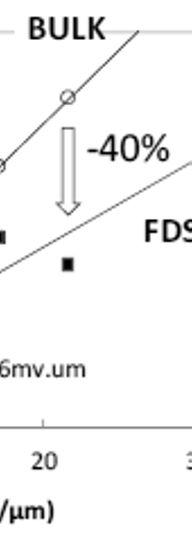
root of device ssion in the ced by 40% [PLA 12])
One have un variabil dopant f devices large ga
Figu FDSOI
last point to doped or lo ity with resp luctuations is reduced in has restor re 1.12 prov [BOE 13].
be highligh w doped ch ect to bulk t (RDF), as sh by 40% in ed SRAM fu
ted is the fa annels. In tu echnology d own in Figu FDSOI as c nctionality
ides a SEM
observatio
CMOS Devices
ct that both rn, it transl due to the su ure 1.11. The compared to and allowed on of STMic
Figur 28 n
e 1.12. SEM o m FDSOI tec
1.2.5. P
Alth establish (FinFET than for (limitati gate pat
atterning
challenges
ough the Fin ed conventi active area their planar on of silico terning.
Amo device years in physics Moore’s Moore’s about 1
FET fabrica onal CMOS ) and the g counterpar n consumpti
bservation of hnology (from for FinFE tion process processes [J ate requires t. While for on without
STMicroelec m Boeuf [BOE
Through the Y FinFET and ates to an im ppression of variability bulk devic for lowered roelectronics tronics 13])
ET and FDS
OI
Years 15 d FDSOI mproved random of small ces. This Vmin.
ng these pro realization t semiconduc and chemist law. With law would micron.
cesses, plas oday. Indee tors manufa ry. Plasma out the com have falter
ma etch tec d, plasma e cturing, con etching has pensating ed around 1
s reuses a la UR 09], the s a much tig the FDSOI damage) of hnology is k etching, used nfronts the fu long enabled capabilities 980 when t
rge part of t patterning o hter process device, the the SOI is ey to the su for more ndamental the perpetu of plasma ransistor siz
s 28 nm the wellof the fin control integrity keyafter
uccess of than 40 limits of uation of etching, es were