

https://ebookmass.com/product/plasma-etching-processes-forcmos-devices-realization-1st-edition-nicolas-posseme/

Checkmate to Murder: A Second World War Mystery E.C.R.
https://ebookmass.com/product/checkmate-to-murder-a-second-world-warmystery-e-c-r-lorac/
ebookmass.com


Plasma Etching Processes for CMOS Device Realization
First published 2017 in Great Britain and the United States by ISTE Press Ltd and Elsevier Ltd
Apart from any fair dealing for the purposes of research or private study, or criticism or review, as permitted under the Copyright, Designs and Patents Act 1988, this publication may only be reproduced, stored or transmitted, in any form or by any means, with the prior permission in writing of the publishers, or in the case of reprographic reproduction in accordance with the terms and licenses issued by the CLA. Enquiries concerning reproduction outside these terms should be sent to the publishers at the undermentioned address:
ISTE Press Ltd
27-37 St George’s Road
Elsevier Ltd
The Boulevard, Langford Lane London SW19 4EU Kidlington, Oxford, OX5 1GB UK UK
www.iste.co.uk
www.elsevier.com
Notices
Knowledge and best practice in this field are constantly changing. As new research and experience broaden our understanding, changes in research methods, professional practices, or medical treatment may become necessary.
Practitioners and researchers must always rely on their own experience and knowledge in evaluating and using any information, methods, compounds, or experiments described herein. In using such information or methods they should be mindful of their own safety and the safety of others, including parties for whom they have a professional responsibility.
To the fullest extent of the law, neither the Publisher nor the authors, contributors, or editors, assume any liability for any injury and/or damage to persons or property as a matter of products liability, negligence or otherwise, or from any use or operation of any methods, products, instructions, or ideas contained in the material herein.
For information on all our publications visit our website at http://store.elsevier.com/
© ISTE Press Ltd 2017
The rights of Nicolas Posseme to be identified as the author of this work have been asserted by him in accordance with the Copyright, Designs and Patents Act 1988.
British Library Cataloguing-in-Publication Data
A CIP record for this book is available from the British Library Library of Congress Cataloging in Publication Data
A catalog record for this book is available from the Library of Congress
ISBN 978-1-78548-096-6
Printed and bound in the UK and US
4.3. Stopping
4.3.1. Foot/notch
4.3.2. Selectivity issues with thin SiO2 and silicon
4.3.3. Selectivity/residues with high-k
4.4. High-k
4.5. Line
4.6. Chamber wall
FinFET sub-20 nm devices, nanowires and stacked nanowires at long term), plasma etching requirements have become more and more stringent with critical dimension control, profile control and film damage at the atomic scale to reach zero variability (precise control of the gate transistor dimension with no damage) required at the horizon of 2020 according to the ITRS.
Now more than ever, plasma etch technology is used to push the limits of semiconductor device fabrication into the nanoelectronics age. This will require improvements in plasma technology (plasma sources, chamber design, etc.), new chemistry methods (etch gases, flows, interactions with substrates, etc.) as well as a compatibility with new patterning techniques such as multiple patterning, EUV lithography, direct self-assembly (DSA), e-beam lithography or nanoimprint lithography.
The goal of this book is to present these etch challenges and associated solutions encountered through the years for transistor realization.
After an introduction to the evolution of CMOS devices through the years in Chapter 1, we will define in Chapter 2 the plasma etching in microelectronics. Then, in Chapter 3, we will present patterning challenges in microelectronics and how plasma etch technology becomes a key solution. Finally, in Chapter 4, we will present the challenges and constraints associated with transistor manufacturing.
Nicolas
POSSEME October 2016
The the “po metal p


Fi pat


gure 1.1. Sch ented transist

Figure 1.2. by Bard first demons int contact” late. The cry


ematics of Lil or (from E.J. L

Artifact of the een, Shockley tration of a transistor m stal was co


ienfeld’s origin Lilienfeld [LIL

first point co and Brattain
ontact transisto n in 1947 in Be
semiconduc ade out of ntacted by
tor-based am a germanium a gold strip al 25])
r fabricated lls Labs plifying dev crystal lyi cut into tw ice was ing on a o pieces

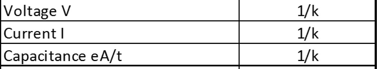

Table 1.1. Scaling results for circuit performance (from B. Dennard et al. [DEN 74])
During the 1970s and 1980s, the semiconductor industry managed to maintain a fast pace and introduced new technology generations approximately every 3 years. This translated into a transistor density improvement of ~2x every 3 years, but this was also a period when average chip size was increasing, resulting in a transistor count increase of close to 2x every 18 months. Starting in the mid-1990s, the semiconductor industry accelerated the pace of introducing new technology generations once every 2 years. Today, the trend of increasing chip size has slowed down slightly due to cost constraints.
Historically, the transistor power reduction afforded by Dennard scaling allowed manufacturers to drastically raise clock frequencies from one generation to the next, without significantly increasing the overall circuit power consumption.
Since around 2005–2007, scaling faced a challenge that broke down Dennard’s scaling law. On reaching 100 nm (or the deep sub-micron channel length), maintaining the electrostatic integrity of the transistor became a major issue.
Some of the major problems to MOSFET scaling in sub-100 nm channel length regime were:
1) short channel effect (SCE);
2) drain induced barrier lowering (DIBL);
accepted as a promising technique to overcome this mobility degradation and to restore CMOS performance to the 90 nm node.
One key consideration in using strain engineering in CMOS technologies is that PMOS and NMOS respond differently to different types of strain. Specifically, PMOS performance is best served by applying compressive strain to the channel, whereas NMOS benefit from tensile strain (see Figure 1.3). Many approaches to strain engineering induce strain locally, allowing both n-channel and p-channel strain to be modulated independently.
The first approach to be introduced involved the use of a strain-inducing capping layer. Chemical vapor deposition (CVD) silicon nitride was a common choice for a strained capping layer, in that the magnitude and type of strain (e.g. tensile vs. compressive) may be adjusted by modulating the deposition conditions, especially temperature. Standard lithography patterning techniques were used to selectively deposit either tensile or compressive strain-inducing capping layers on either N or PMOS.
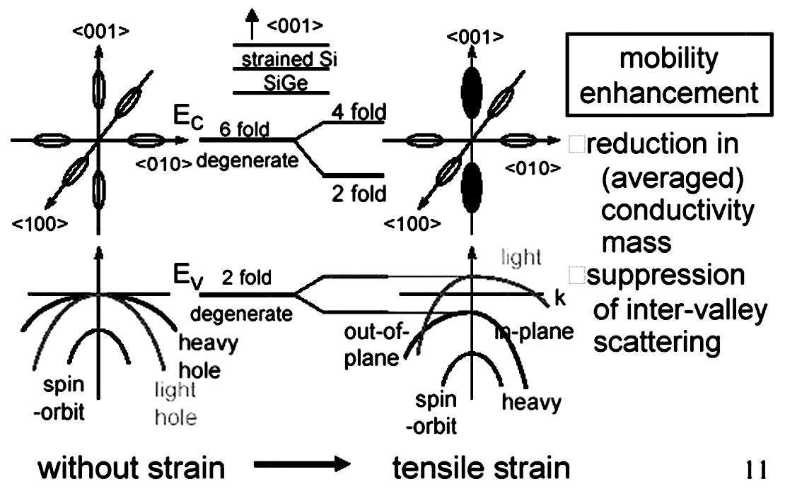
Figure 1.3. NMOS band diagram with and without tensile strain. Tensile strain induces a degeneracy splitting in the <001> valleys. As a result, the electron concentration increases in the low effective mass subbands, resulting in a lowered averaged conductivity mass (from S-I. Takagi [TAK 03])
A second prominent approach in strain engineering involves the use of silicon-rich alloys, especially silicon-germanium, to modulate channel strain. For instance, compressive strain can be induced by replacing the source and drain region of a MOSFET with silicon-germanium (Figure 1.4).


Figure 1.4. Intel 65 nm technology corresponding to the second generation of uniaxial strained Si for enhanced performance (Lg = 35 nm, Tox = 1.2 nm) (adapted from S. Thompson [THO 05])
1.2.2. Leakage current reduction
The scaling of silicon dioxide dielectrics was an effective approach to enhance transistor performance in complementary metal–oxide–semiconductor (CMOS) technologies as predicted by Moore’s law (see equation [1.1]).
In the past few decades, a reduction in the thickness of silicon dioxide gate dielectrics has enabled increased numbers of transistors per chip with enhanced circuit functionality and performance at low costs. However, as the devices approach the sub-45 nm scale, the equivalent oxide thickness (EOT) of the traditional silicon dioxide dielectrics is required to be smaller than 1 nm, which is approximately 3 monolayers and close to the physical limit, resulting in high gate leakage currents due to the obvious quantum tunneling effect at this scale.
Figure 1.5 shows how gate leakage becomes the main contributor to leakage current when the equivalent oxide thickness was scaled down in the 1.5 nm range.
The as illust thin equ F of t i 1.2.3. G
of metal ga re 1.7. Poly e thickness.


igure 1.7. Sch he example) p ncrease of th ate-last ap
ematics of th olysilicium ga e gate oxide t control of t proach
omitantly w on scheme w
Indeed, the P etal undergo metal gate s also known scene proces mptied after re 1.8 repres gate patte on (Figure 1 ical mecha gate is selec high-k–wo gate (tungs ation step (F
Conc integrati PFETs. as the m Vt, the process, a Dama will be e Figu dummy realizati by chem dummy Finally, metal planariz introduction rated in Figu ivalent oxid
te stack sup depletion w e polydepletio te. This polyd hickness, resu he gate over t
ith the highas changed -type workes thermal b tack is depo as the replac s where a d RSD definit
ents a simpl rning using .8(a)), a sili nical polish tively remo rk-function ten) are d igure 1.8(f))

pressed the p as on the wa on effect in a N depletion resu ulting in a low he channel
Through the Y olydepletio y to benefiti + (for the sak lts in an appa er electrostati
e stack introd irst to gate-l ds to get mo Thus, in order unction acti l gate proces is used to d UI 02] for ear e of the gate entional ap film is depo 1.8(b)). In g a cavity in ) (Figure 1 Figure 1.8(e
k/metal gate from gate-f function ten udgeting. T sited after j ement meta ummy gate ion (see [GU ified scheme the conv con dioxide ing (Figure ved, creatin metal (TiN eposited (F . CMOS Devices
uction, the g ast to ensure re and more to target lo vation. The s (RMG), co efine a cavit ly work).
-last approac proach and sited and pl Figure 1.8 the silicon .8(d)) and )) followed
Years 11 on effect, ing from ke arent ic gate stack low Vt mid-gap ow PFET gate-last nsists of y which ch. After d spacer lanarized 8(c), the dioxide. capping d by a


1.2.4. New transistor generations
1.2.4.1. FinFET
The most dramatic change in CMOS transistors was brought by Intel at 22 nm node, in the year 2011, with the introduction of FinFET architecture in production. FinFET devices belong to the fully depleted architectures (sometimes this statement can be argued depending on the junction isolation to the bulk substrate) like FDSOI, Gate-all-Around transistors and all the architectures where we can define a silicon thickness or width that is smaller than the depletion depth in the device. The architectures of the fully depleted family are shown in Figure 1.9.
The fully depleted architectures were introduced to restore the gate electrostatic control over the channel. Indeed when the gate length became shorter than 30 nm, it becomes extremely challenging for bulk planar devices to maintain low Ioff currents, in spite of very high channel doping and the use of halos (highly doped pockets at the entrance of the channel, of opposite channel type, designed in order to enhance the potential barrier at the source side).
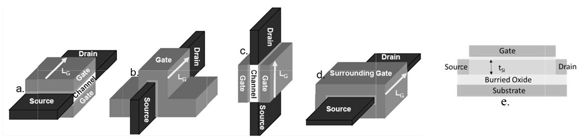
Figure 1.9. (a) Planar DG [BAL 87], (b) FinFET [HIS 89], (c) vertical surrounding gate [TAK 88], (d) gate all around (GAA) [COL 90], (e) thin film transistor on top of a buried oxide with a ground plane (from M. Fukuma [FUK 88])
Electrostatics in fully depleted architectures is controlled by the thin silicon film channel thickness or the Fin width. As shown in equation [1.2], the DIBL (and subthreshold slope) improves for a given gate length as a function of thinner silicon channel thickness or thinner Fin width as implemented in the Mastar model [SKO 93], which was the analytical model used to build ITRS specifications:
Figure 1.10 provides some SEM observations of Intel 22 nm FinFET. The fact that the active width is now discrete (a multiple of the number of Fin) appears clearly.
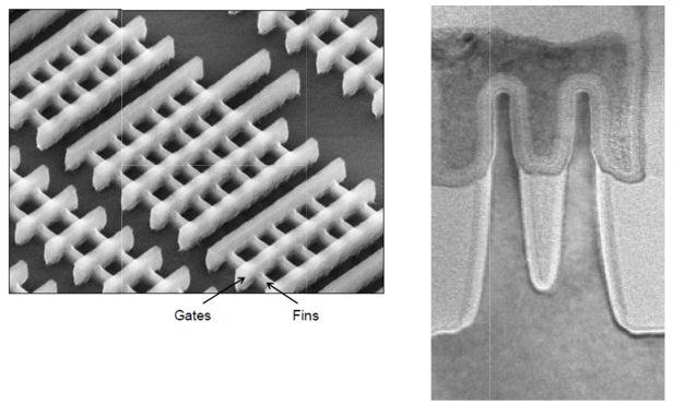

Figure 1.10. Left: top-down SEM observation of Intel 22 nm FinFET technology (from http://www.intel.com/content/www/us/en/silicon-innovations/intel-22nmtechnology.html). Middle: 14 nm Fin cross-section. Right: first metal levels cross-section (from S. Natarajan [NAT 14])