All rights reserved. No part of this publication may be reproduced, stored in a retrieval system, or transmitted, in any form or by any means, electronic, mechanical, photocopying, recording or otherwise, except as permitted by law. Advice on how to obtain permission to reuse material from this title is available at http://www.wiley.com/go/permissions.
The right of Tim Bruton to be identified as the author of this work has been asserted in accordance with law.
Registered Offices
John Wiley & Sons, Inc., 111 River Street, Hoboken, NJ 07030, USA
John Wiley & Sons Ltd, The Atrium, Southern Gate, Chichester, West Sussex, PO19 8SQ, UK
Editorial Office
The Atrium, Southern Gate, Chichester, West Sussex, PO19 8SQ, UK
For details of our global editorial offices, customer services, and more information about Wiley products visit us at www.wiley.com.
Wiley also publishes its books in a variety of electronic formats and by print‐on‐demand. Some content that appears in standard print versions of this book may not be available in other formats.
Limit of Liability/Disclaimer of Warranty
While the publisher and authors have used their best efforts in preparing this work, they make no representations or warranties with respect to the accuracy or completeness of the contents of this work and specifically disclaim all warranties, including without limitation any implied warranties of merchantability or fitness for a particular purpose. No warranty may be created or extended by sales representatives, written sales materials or promotional statements for this work. The fact that an organization, website, or product is referred to in this work as a citation and/or potential source of further information does not mean that the publisher and authors endorse the information or services the organization, website, or product may provide or recommendations it may make. This work is sold with the understanding that the publisher is not engaged in rendering professional services. The advice and strategies contained herein may not be suitable for your situation. You should consult with a specialist where appropriate. Further, readers should be aware that websites listed in this work may have changed or disappeared between when this work was written and when it is read. Neither the publisher nor authors shall be liable for any loss of profit or any other commercial damages, including but not limited to special, incidental, consequential, or other damages.
Library of Congress Cataloging‐in‐Publication Data
Names: Bruton, Tim, 1946– author.
Title: Photovoltaics from milliwatts to gigawatts : understanding market and technology drivers toward terawatts / Tim Bruton.
Description: Hoboken, NJ : Wiley, 2021. | Includes bibliographical references and index.
Identifiers: LCCN 2020030557 (print) | LCCN 2020030558 (ebook) | ISBN 9781119130048 (cloth) | ISBN 9781119130055 (adobe pdf) | ISBN 9781119130062 (epub)
Subjects: LCSH: Silicon solar cells. | Photovoltaic power generation–History. | Photovoltaic power systems. | Solar energy industries.
Set in 10/13pt STIXTwoText by SPi Global, Pondicherry, India
For my grandchildren:
Bethan, Benjamin, Carys, Daniel, Isaac, Jemima, Joseph, Joshua, Samuel
Contents
Preface xii
1 The Photovoltaics: The Birth of a Technology and Its First Application 1
1.1 Introduction 1
1.2 Sunlight and Electricity 2
1.2.1 The Early Years 2
1.2.2 The Breakthrough to Commercial Photovoltaic Cells 4
1.2.3 Hiatus 7
1.2.4 The First Successful Market: Satellites 8
1.3 Photovoltaics Demonstrates Success 9
1.3.1 First Commercial Operation 11
1.3.2 Continuing Research for Space 13
1.3.3 Solar Cell Manufacturing 15
1.4 Gallium Arsenide and III–V Alloys for Space 16
1.4.1 Single-Junction GaAs Solar Cells 17
1.4.2 Multijunction Solar Cells for Space 18
1.5 Summary 20 References 21
2 The Beginnings of a Terrestrial Photovoltaics Industry 25
2.1 Introduction 25
2.2 The 1973 Oil Crisis 26
2.3 The Way Ahead for Terrestrial Photovoltaics Technology 27
2.3.1 Basic Silicon Photovoltaic Manufacturing Process 29
2.3.2 The Flat Plate Solar Array Project 30
2.3.2.1 Solar-Grade Silicon 30
2.3.2.2 Silicon-Sheet Wafers and Ribbons 30
2.3.2.3 High-Efficiency Solar Cells 30
2.3.2.4 Process Development 31
2.3.2.5 Engineering Sciences and Reliability 31
2.3.2.6 Module Encapsulation 33
2.3.2.7 Cost Goals 33
2.4 Rise of the US Photovoltaic Manufacturing Industry 34
2.5 Developments in Europe 35
2.6 The Transition in Cell Technology from Space to Terrestrial Applications 36
2.7 Alternatives to Silicon for Solar Cells 39
2.8 Summary 40
References 41
3 The Early Photovoltaic Global Market and Manufacturers 43
3.1 Introduction 43
3.2 Off- Grid Professional Market 45
3.2.1 Navigation Aids 45
3.2.2 Microwave Repeater Stations 46
3.2.3 Cathodic Protection 48
3.2.4 Other Applications 49
3.2.5 Early Grid- Connected Application 51
3.3 Off- Grid Domestic Market 53
3.3.1 Solar Home Systems 54
3.3.2 Water Pumping 56
3.3.3 Consumer Electronics 57
3.4 Summary 59
References 59
4 Silicon Technology Development to 2010 61
4.1 Introduction 61
4.2 Technologies Supplying the Global Market 61
4.3 Advantages of Silicon as a Solar Cell Material 62
4.3.1 Readily Available 62
4.3.2 Elemental Semiconductor 63
4.3.3 Nontoxic 63
4.3.4 Self-Passivating Oxide 63
4.3.5 Synergy with the Global Semiconductor Industry 63
4.4 Silicon Solar Cell Design Features 64
4.5 Silicon Solar Cell Manufacturing from 1980 to 1990 67
4.5.1 Silicon Feedstock 68
4.5.2 Crystallisation 72
4.5.3 Wafering 76
4.5.4 Antireflection Coating 78
4.6 Solar Cell Development to 2000 79
4.6.1 CZ Cell Development 79
4.6.2 Multicrystalline Silicon Processing 82
4.6.3 Integration of Mono- and Multicrystalline Silicon Processes 83
4.6.4 Other Process Technology Changes 84
4.7 Module Technology 85
4.8 Summary 87 References 87
5 Evolution of Photovoltaic Systems 91
5.1 Introduction 91
5.2 The Off- Grid Market 93
5.3 The Decentralised Grid- Connected Market 96
5.3.1 The Research Phase: 1974–1989 97
5.3.2 The Demonstration Phase: 1989–2000 97
5.3.3 The Commercial Phase: 2000–2019 100
5.3.3.1 Achievement of Grid Parity 105
5.3.3.2 Resolution of the Silicon Feedstock Supply 106
5.4 Utility-Scale Grid- Connected Photovoltaic Systems 109
5.5 Novel Applications 112
5.6 Summary 113 References 113
6 History of Incentives for Photovoltaics 115
6.1 The Chicken and Egg Problem 115
6.2 Capital Subsidies on System Purchase 116
6.3 Feed-in-Tariffs 118
6.4 Power Purchase Agreements and Other Incentives for Large-Scale Systems 122
6.5 Summary 127 References 128
7 Difficulties of Alternative Technologies to Silicon 129
7.1 Introduction 129
7.2 Sheet Silicon Processes 129
7.2.1 Direct Crystallisation of Silicon Sheet 130
7.2.1.1 Westinghouse Dendritic Web 130
7.2.1.2 Edge Defined Foil Growth 130
7.2.1.3 String Ribbon Technology 132
7.2.2 Cast Silicon Sheet 133
7.2.2.1 Hoxan Casting Process 133
7.2.2.2 Ribbon Growth on Substrate 133
7.2.2.3 Direct Wafer 134
7.2.2.4 Lift-Off Wafer Technology 135
Contents x
7.3 Thin-Film Solar Cell Technologies 135
7.3.1 Copper Sulphide 136
7.3.2 Amorphous Silicon 137
7.3.2.1 Amorphous Silicon Manufacturing 140
7.3.2.2 Manufacture of the Amorphous Silicon Microcrystalline Silicon Tandem Cell 143
7.3.3 Thin-Film Crystalline Silicon 144
7.3.4 Copper Indium Gallium Diselenide (CIGS) 146
7.3.4.1 CIGS Manufacturing 149
7.3.5 Cadmium Telluride 151
7.3.5.1 Cadmium Telluride Manufacturing 152
7.3.6 Dye-Sensitised Solar Cells 154
7.3.7 Polymer (Organic) Solar Cells 156
7.3.8 Perovskite Solar Cells 157
7.4 Concentrator Technologies 159
7.5 Summary 161
References 162
8 Current Status of Crystalline Silicon Manufacturing and Future Trends 168
8.1 Introduction 168
8.2 Approaches to High-Efficiency Silicon Solar Cells on p Type Silicon Wafers 169
8.2.1 LGBC Solar Cells 169
8.2.2 Selective Emitters 171
8.2.3 PERL and PERC Solar Cells 171
8.2.4 Industrial Manufacture of PERC Cells 177
8.2.5 Bifacial Module Technology 178
8.2.6 Light-Induced Degradation 180
8.3 Solar Cells with n Type Silicon 182
8.3.1 SHJ Solar Cells 182
8.3.2 IBC-SHJ Solar Cells 184
8.3.3 n Type IBC Cells Without Amorphous Silicon Passivation 185
8.4 The Future of Photovoltaic Technology: Toward Terrawatts 188
8.4.1 III–V Tandems on Silicon 189
8.4.2 Silicon Tandems Using Perovskites 190
8.5 Silicon Module Reliability 192
8.6 Summary 192
References 194
9 Lessons Learnt 199
9.1 Introduction 199
9.2 Role of Governments 200
9.3 Role of the Research Community 202
9.4 Role of the Manufacturing Industry in Europe and the United States 203
9.5 Role of China as a Photovoltaics Manufacturing Base 205
9.6 Potential for Continued Market Growth 206
9.7 Future Technology Development 208
9.8 Final Analysis 209
References 210
Index 213
Harnessing the power of the sun has been a challenge to the human race for thousands of years. In the last quarter of the twentieth century and into the twenty‐first, the deployment of photovoltaic solar energy conversion assumed great importance. In its early years, it promised security of energy supply and price stability for many countries, and today it is a reliable route to carbon‐free energy production, a vital tool in the fight to halt manmade climate change. I have been highly privileged in being able to see this dramatic story evolve. I joined the embryonic BP Solar research team in August 1983 when the world market was a mere 20 megawatts and the future uncertain. In the subsequent 37 years, I have seen the technology grow from those early days when many applications were at the milliwatt scale to now, when single photovoltaic power stations of over 1 GWp are in operation. That this has happened is due to the interactions of many actors from the fields of science, manufacturing, and politics.
My ambition in this book is to relate how solar cells transitioned from a high‐cost, small‐volume, niche market to the global status they enjoy today. The text follows the developments in fundamental understanding, cell processing, and scale‐up of manufacturing (and subsequent drop‐off in product cost). I tend to use the conversion efficiency of solar cells from solar radiation to useful electricity as a criterion for assessing the progress of particular technologies, but with the caveat that high efficiency must be achieved cost‐effectively. Throughout the period in question, I was principally involved at BP Solar and then at NaREC in silicon solar cell design and manufacturing, although along the way I also had responsibilities for thin‐film silicon, cadmium telluride, III‐V cells, and concentrators. I have taken the opportunity to detail progress in these areas, but also to give my own explanation for why they have not been able to displace silicon as the prime solar cell material. The opinions expressed in this book are entirely my own and are not the views of any of my previous employers.
Throughout my career, I had the privilege of working with many able and dedicated people. In particular, I am indebted to Nigel Mason, Stephen Roberts, Daniel Cunningham, Keith Heasman, and Stephen Ransome for their steadfast support and friendship through the years. Following the merger of BP Solar with Solarex in 2000, I was able to connect with a different generation of pioneers, and it was inspiring to be Preface
Preface
able to share ideas with Steve Shea, John Wohlgemuth, and the late David Carlson. I have also enjoyed interactions with many others through supporting manufacturing in the United Kingdom, Spain, India, Australia, and the United States. There are many other colleagues from my time in BP Solar and NaREC who helped in innumerable ways, and space does not allow me to acknowledge them all by name. I must thank my wife, Margaret, who selflessly supported me throughout my career and without whom this book would not have been written.
1
The Photovoltaics: The Birth of a Technology and Its First Application
1.1 Introduction
‘For more than a generation, solar power was an environmentalist fantasy, an expensive and impractical artefact from the Jimmy Carter era. That was true right up to the moment it wasn’t’ [1]. This quotation neatly encapsulates the theme of this book: how a technology grew from a high‐cost product in a specialist application to a global technology supplying a significant proportion of the world’s electricity against a background of at best scepticism and at worst open hostility. In 2018, 102 GWp of photovoltaic modules were installed globally, leading to a total installed capacity of 509 GWp, while an independent study showed that photovoltaics was the lowest‐cost means of generation of new‐build electricity‐ generating capacity, including nuclear and fossil fuel sources [2]. At the end of 2019, photovoltaics provided 3% of the global electricity supply, but the expectation is that this percentage will continue to rise until it is the dominant electricity‐generating technology by 2050, with 60% of global output [3,4]. Figure 1.1 shows the expected growth of all generating technologies to 2050. This dramatic development of photovoltaic installations has been the work of many inspired individuals. Their stories are told in other places [5–7]. The aim of this book is to describe how the technology changed from small‐area solar cells of 10% efficiency conversion of sunlight to electricity to the mass‐production cells of today, with efficiencies in the range 20–24%, and the route to >30% becoming clear. The present chapter describes how the potential for photovoltaic conversion was first recognised and how it moved into the early stages of commercialisation as a high‐technology product for use in powering space satellites. Later chapters will describe how this space technology became a terrestrial one and the driving forces and technology developments that made it the global force it is today. Furthermore, the options for going beyond the current technology will be reviewed and the route to achieving terawatt global installations discussed. It should be no surprise that photovoltaics has achieved the advances it has. Since the invention of the semiconductor transistor in 1948, solid‐state electronics has transformed the way in which we live. Computers, mobile phones, the Internet, and so much
Photovoltaics from Milliwatts to Gigawatts: Understanding Market and Technology Drivers toward Terawatts, First Edition. Tim Bruton.
Figure 1.1 Evolution of electricity-generating technologies to 2050 Source: DNV GL Energy
Transition Outlook 2018
else would not exist without the underlying semiconductor technology. Photovoltaic solar energy conversion is the application of solid‐state technology to the energy field. Electricity is generated simply by the absorption of sunlight in a semiconducting diode. There are no moving parts. No liquid or gaseous fuels are needed. There are no effluents requiring disposal and no noise is generated. Sunlight is abundant, delivering to the earth’s surface 6000 times humanity’s total energy usage [8]. It is the only renewable resource capable of delivering the world’s energy needs carbon‐free by 2050, and it will remain available for the next 5 billion years. The photovoltaic technology is easily scalable, so that small cells can generate the few milliwatts required for consumer devices such as calculators and watches, while larger ones can be used to assemble modules for deployment at the gigawatt level. It is these advantages which spurred many advocates to continue to promote photovoltaics in the face of significant opposition.
1.2 Sunlight and Electricity
1.2.1
The Early Years
While the potency of the sun has been recognised from ancient times, its role has been mainly that of a source of heat and lighting [9]. It was only relatively recently that the connection between sunlight and electricity was established. Through the nineteenth century, there was an important discovery in this regard about once every decade. Probably the first connection between light and electricity was made by Edmond Becquerel in Paris in 1839 [10]. He observed the flow of an electric current when gold or platinum electrodes were immersed into an electrolyte (acidic or alkaline) and exposed to uneven solar radiation. Some ten years later, Alfred Smee in London observed a current in an electrochemical cell on exposure to intense light, which he called a ‘photo‐voltaic’ circuit – linking the Greek word for light phos and the name ‘Volta’, the original inventor of the galvanic cell [11].
The next step was the observation of photoconductivity in a solid material. A British engineer, Willoughby Smith, in search of a high‐resistance metal for use in testing the trans‐Atlantic telegraph cable, was recommended selenium. He purchased some selenium rods of between 5 and 10 cm in length and 1 and 1.5 mm in diameter [12]. These were hermetically sealed in glass cylinders, with leads to the outside. They worked well at night, but in bright daylight they became too conducting. Smith concluded that there was no heating effect and that the change in resistance was purely due to the action of light [13]. This stimulated further research into the properties of selenium. The British scientists William Grylls Adams and Richard Evans Day observed current flowing in their selenium sample when no external voltage was applied and were able to show that ‘a current could be started in the selenium by the action of light alone’ [14]. They had demonstrated for the first time that light caused the flow of electricity in a solid material. They used the term ‘photoelectric’ to describe their device, and Adams believed it could be used as a means of measuring light intensity [15].
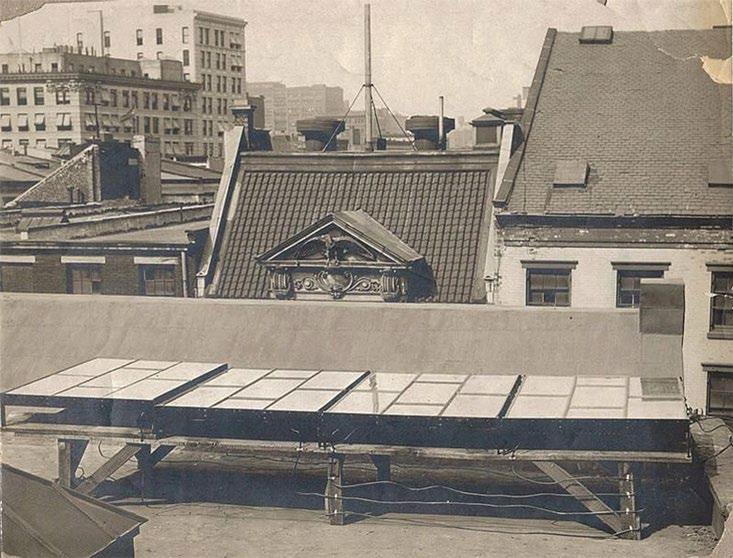
The narrative now switches to America, where Charles Fritts made the first working solar module by covering a copper plate with a layer of selenium and applying a semitransparent gold layer as the top electrode [16]. An example is shown in Figure 1.2. Fritts described the module as producing a ‘current that is constant and of considerable force . . . not only by exposure to sunlight but also to dim diffused light and even to
Figure 1.2 Charles Fritts’ first photovoltaic array, produced in New York City in 1884 [16] (Courtesy New World Library)
Photovoltaics from Milliwatts to Gigawatts 4 lamplight.’ He supplied samples to the German electricity pioneer Werner von Siemens, who greeted them enthusiastically, announcing Fritts’ module to be ‘scientifically of the most far‐reaching importance’. However, its low efficiency – below 1% – made it of little commercial importance. Indeed, there was considerable scepticism at the time, with solar cells viewed as some kind of perpetual‐motion machine. The principles of their operation were not understood. One of the leading physicists of the day, James Clerk Maxwell, while welcoming photoelectrcity as ‘a very valuable contribution to science’, wondered ‘is the radiation the immediate cause or does it act by producing some change in the chemical state’ [16].
The underlying science of photovoltaics was given a big boost by the parallel discoveries and developments in photoemission. Hertz observed in 1887 that ultraviolet light caused a significant increase in the sparks in an air gap between electrodes and that it was a function of the wavelength of the light rather than its intensity [17]. While a number of physicists worked on the effect, it was Albert Einstein in 1905 who explained it in terms of different wavelengths behaving as particles of energy, which he called ‘quanta’ but which were later renamed ‘photons’. These quanta had different energies depending on their wavelength. Einstein was awarded the Nobel Prize in 1921 for this work [15]. While these discoveries and other advances in quantum mechanics at the start for the twentieth century did not directly explain photovoltaic effects, they did provide a scientific basis for understanding the interaction of light and materials.
Although research continued on developing solar cells, little progress was made. However, photovoltaics still had its advocates in the 1930s. Ludwig Lange, a German physicist, predicted in 1931 that ‘in the distant future huge plants will employ thousands of these plates to transform sunlight into electric power . . . that can compete with hydroelectricity and steam driven generators in running factories and lighting homes’ [15]. A more pragmatic view was taken by E.D. Wilson at Westinghouse Electric, who stated that the efficiency of the photovoltaic cell would need to be increased by a factor of 50 in order for them to be of practical use, and this was unlikely to happen [15]. Actually, as will be shown in later chapters, a factor of 20 was achieved, and this was sufficient to create the current global markets.
While progress in other areas of technology was immense in the nineteenth and early twentieth centuries, little real advancement in photovoltaics had been made since Becquerel’s discovery a hundred years previously. Entering into the second half of the twentieth century, everything would change.
1.2.2 The Breakthrough to Commercial Photovoltaic Cells
It is well known that the birth of the commercially successful photovoltaic cell dates back to April 1954, when Pearson, Chapin, and Fuller demonstrated the first 6% efficient cell using a p/n junction in silicon. It is no surprise that this discovery occurred at Bell Telephone Laboratories, which was one of the world’s premier research laboratories until its forced break‐up in 1984. As the research arm of the American Telephone
and Telegraph Company, it had a long history of successful innovation, with nine Nobel Prizes awarded over time for work done there. Perhaps its most notable success was the demonstration in 1948 of the point‐contact germanium transistor. This illustrates the strength and depth of both the theoretical understanding and expertise in semiconductor processing at Bell labs [18].
Figure 1.3 Ohl’s patented solar cell structure [20] Source: R.S. Ohl: US Patent Application filed 27th May 1941
Russel Ohl, a Bell Labs scientist interested in exploring the crystallisation of silicon, is recognised as the discoverer of the p/n junction in this material, in 1941 [19]. In directionally solidifying 99.85% pure silicon, Ohl noted a change in the structure of the solidified ingot, with the upper portion becoming columnar and the lower portion showing no structure; a striated region appeared between the two, forming a barrier to conduction. The upper zone was p type while the lower zone was n type [20]. This can be easily understood as a result of the segregation of dopants during the crystallisation process. While measuring the resistance of rods containing the barrier, Ohl noted a sensitivity to light, which he termed a ‘photo electromotive force’. He proceeded to patent this as a solar cell, although its efficiency was similar to that of the selenium cells, at about 1% [20]. Figure 1.3 shows Ohl’s silicon structure, the n type region being fine‐grained crystallites and the cell contacts plated rhodium. The low efficiency is not surprising given the relatively impure starting material, its multicrystalline nature, and the fact that the n type region was 0.5 mm thick. The relatively low efficiency meant little further work was done until a new approach at Bell Labs.
Success came in the 1950s. The first transistor had been demonstrated at Bell in 1948 using germanium, and had entered commercial production in 1951 [21]. However, germanium had some disadvantages in its fragility and stability, and silicon offered a better option – although a working silicon transistor was not demonstrated until 1954. Two scientists working on this were Calvin S. Fuller and Gerald L. Pearson. Fuller was an expert in doping silicon, while Pearson was an experimentalist. There were three iterations before a good working solar cell was demonstrated [22]. Initially, while not looking for a solar cell, Fuller produced a p type gallium‐doped silicon sample, which Pearson dipped into a lithium bath to form a shallow n type region. When Pearson exposed the sample to light, he found to his surprise that a current was generated. At the same time, in a different department, another scientist, Daryl M. Chapin, was looking for a power source for telecommunications repeaters in hot humid locations where conventional dry cell batteries rapidly failed. Chapin concluded that solar cells were a good option, but his experiments with commercial selenium cells of low efficiency were disappointing. He and Pearson knew each other, and Pearson offered Chapin his lithium‐doped ‘solar cell’. Chapin tested it and found it 2.3% efficient – an enormous
improvement on selenium, justifying further investigations into silicon’s potential. The next step was to replace the lithium with phosphorus. A small amount of phosphorus was evaporated on to the p type silicon to make a shallow n type region. Initial results weren’t particularly good, but then Chapin applied a thin plastic layer to act as an antireflection coating (ARC) on the otherwise highly reflecting silicon surface. This gave the encouraging result of around 4% cell efficiency, which was good progress toward Chapin’s target of 5.7% for a viable power source. However, further progress was slow, and forming a good electrical contact proved to be an ongoing problem. A spur to further activity came from Bell’s competitor, RCA, which was developing an ‘atomic battery’ using a strontium 90 source to irradiate a silicon solar cell, although efficiencies were poor. The breakthrough came when Fuller, who had been experimenting with boron to give a p type silicon emitter which offered a new configuration, demonstrated that heating an n type silicon wafer for 5.5 hours at 1000 °C in a boron trichloride atmosphere under reduced pressure could produce a 0.25 μm‐deep diffusion with a resistivity of .001 Ω/cm [23]. This equated to 40 Ω per square sheet resistance emitter, which is a typical figure for later commercial silicon solar cells. Arsenic was used to dope the silicon base n type to 0.1 Ω/cm, and this was then cut into long narrow strips in accordance with the best previous cell results. The emitter was formed using the new boron diffusion process, with the emitter itself wrapping around the cell as shown in Figure 1.4. It was then partially removed on the rear to expose the n type base. Contacts were made by electroplating rhodium to the exposed base and emitter [24]; the relative ease in forming these contacts represented a significant advance. A polystyrene layer with refractive index 1.6 was used as the ARC. The solar cell efficiency was approximately 6% [25]. Chapin had proposed a theoretical limit of 22% efficiency for silicon, but had stated that practical limitations would result in its being lower in the real world. The spectral response of the cell is shown in Figure 1.5. It was proposed that 10 cells
n type silicon
Boron p type emitter
Anti-refection coating
Rhodium contacts
Figure 1.4 Schematic of the first successful silicon solar cell
Figure 1.5 (A) Normalised spectral response of a p on n silicon solar cell. (B) Solar spectrum. (C) Relative integrated response [23] Source: C.S. Fuller: US Patent 3015590, 2nd Jan. 1962 (filed 5th March 1954)
connected in series would be needed to provide the 1 W of power required to charge the batteries at a repeater station in a rural carrier telephone system [24].
The 6% efficiency result met Chapin’s original target and gave the impetus for further improvement. By November 1954, an 8%‐efficiency cell had been produced with the same wraparound structure [26], and by May 1955, 11% efficiency was demonstrated [27]. It is interesting to note that this structure – an n type wafer with all of the contact metallisation on the rear – has a resonance with the current world‐record silicon solar cell (26.7% efficiency), based on an n type wafer with rear contacts, but with amorphous silicon providing the p side of the junction [28]. In their 1954 patent filing, the inventors stated that ‘Sunlight is the most common, most accessible, and most economical form of energy on the Earth’s surface’ [24]. This group at Bell Labs opened the door for practical exploitation of this rich energy source, although it was a further 20 years before its true potential began to be fully exploited.
1.2.3 Hiatus
While the Bell discovery was heralded as a great breakthrough, with the New York Times stating it ‘may mark the beginning of a new era, leading eventually to the realisation of one of mankind’s most cherished dreams – the harnessing of the almost limitless energy of the sun for the uses of civilisation’ [29] and the US News & World Report claiming ‘the (silicon) strips may provide more power than all the world’s coal, oil and uranium’ [30], the reality in 1954 was somewhat different. The cost of the high‐purity silicon needed to make viable solar cells was very high at $845/kg, resulting in an estimated cost of electricity of $144/kWh, compared to $23.7/kWh for dry cell batteries and less than $0.02/kWh for retail grid electricity [31]. Despite this disadvantage, Bell’s manufacturing subsidiary, Western Electric, took up commercialisation.
Photovoltaics from Milliwatts to Gigawatts 8
One of the first applications was powering a remote telephone line in rural Georgia (USA). However, the introduction of silicon transistors for voice amplification with a very low power requirement made the application redundant and activity at Bell largely declined [31]. Western Electric licensed other companies to manufacture the silicon solar cells, one of which, National Fabricated Products, went as far as to assemble a range of demonstration products. But no market was forthcoming and National Fabricated Products was taken over by Hoffman Electronics in 1956. Hoffman provided prototypes for both the US Coast Guard and the US Forest Service, but no business resulted. The initial enthusiasm cooled to the extent that in 1957 it was reported that ‘Viewed in the light of the world’s power needs, these gadgets are toys’ [32].
1.2.4 The First Successful Market: Satellites
Although a terrestrial market was slow to materialise, Hoffman Electronics continued to do research to improve solar cell efficiency and reduce cost. By the end of 1957, it had demonstrated a 12.5% (1 cm2)‐efficient silicon cell [33]. The discoveries at Bell Laboratories did not pass unnoticed amongst the military, and the US Army Signal Corps visited the company to evaluate the technology and concluded that the only viable application was for the power supply of an artificial earth satellite, which was a top secret project at the time [34]. This view was shared by the US Air Force – but not by the US Navy, which was eventually awarded the satellite project, and which had decided that silicon solar cells were ‘unconventional and not fully established’ [34]. Interdepartmental rivalries also played a part [35]. Nonetheless, when President Eisenhower first announced the satellite programme publicly in 1955, the New York Times published a sketch showing solar cells providing the power. Intense lobbying was carried out, particularly by Dr Hans Ziegler of the Signal Corps Research and Development Laboratory (USARDL), assisted by a decision to simplify the satellite’s mission and lighten its payload. Eventually, it was agreed that both a dry cell battery power supply and a solar‐powered transmitter would be used. Solar cells were tested by attaching them to the nose cones of two high‐altitude rockets and were shown to survive the rigours of the launch and of the space environment.
The first launch in December 1957 of the Vanguard TV‐3 satellite, depicted in Figure 1.6, failed, but the satellite itself was recovered [36]. The Vanguard 1, identical to the TV‐3, was successfully launched on 17 March 1958, with the expectation that it would remain in orbit for 2000 years (although later recalculation lowered this to 240 years). It is the oldest artificial satellite still orbiting the earth. Its scientific purpose as part of the International Geophysical Year was to obtain geodetic measurements of the shape of the planet. As predicted, the battery‐powered transmitter stopped working in June 1958, while the solar‐powered one continued until May 1964, when the last signals were received in Quito, Ecuador. The satellite was a 16.5 cm aluminium sphere weighing 1.48 kg. A 10 mW 108 MHz telemetry transmitter was powered by a set of mercury batteries, while a 5 mW 108.03 MHz beacon transmitter was powered by solar
Figure 1.6 Vanguard TV-3 satellite on display at the Smithsonian Air and Space Museum. Recovered from its failed launch on 6 December 1957 [36] Source: Smithsonian National Air and space Museum (TMS A19761857000cp02)
cells mounted in six 5 × 5 cm arrays, which gave a nominal power of 1 W, equating to an efficiency of 10% at 28 °C [34]. The cells were supplied by Hoffman Electronics. This proved to be a watershed moment for photovoltaics, as the technology had proved itself a reliable long‐term source of electricity in a real application.
1.3 Photovoltaics Demonstrates Success
With the highly visible success of the Vanguard 1 mission, photovoltaics became the technology of choice for powering satellites. Nevertheless, some scepticism remained in place, and photovoltaics was seen purely as a stopgap measure until atomic batteries were developed. Others thought that while photovoltaics was acceptable for the simple early satellites, it would not provide enough power for the more sophisticated ones – not to mention space stations – envisaged for the future [37].
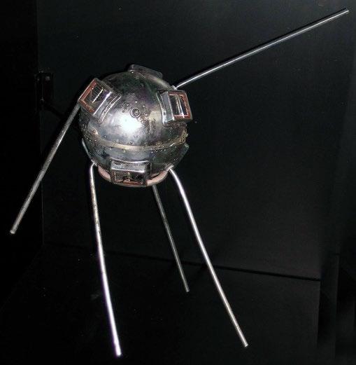
Immediate confirmation of the value of solar cells in space was given by the Russians, who launched the Sputnik 3 on 5 May 1958, also as part of the International Geophysical Year. In addition to a number of scientific instruments, Sputnik 3 included a solar cell‐powered transmitter [38]. The Russians had been monitoring Bell Laboratories’ work and had developed their own cells [37]. One Russian scientist stated in 1958 that ‘Solar batteries . . . would ultimately become the main source of power in space’. With hindsight, it is easy to see how these predictions became true. Space was the obvious market for solar cells. Solar insolation is 40% higher in space than on the earth’s
Photovoltaics from Milliwatts to Gigawatts 10
surface. Satellites are the ultimate off‐grid market, with no maintenance possible after launch until at least the 1990s. They are free of the day–night constraints of terrestrial systems. Price is not an issue, given the high cost of launchings satellites. In any case, with increasing production volume and the general growth of the silicon semiconductor infrastructure, solar cell costs had fallen to $100/W by 1970.
Space offered some challenges, however. It had been noted by RCA Laboratories that in its experiments to produce electro‐voltaic cells, beta radiation from a Sr90‐Y90 source had seriously degraded solar cell performance [39]. Initially, figures for cosmic radiation were extrapolated from high‐altitude balloon flights, and it was calculated that it would take 105 years for there to be a 25% loss of cell efficiency. However, the Explorer 1 satellite, launched in 1958, found that in the yet to be recognised van Allen radiation belt, cosmic radiation was 104 times higher than that estimated from balloons, meaning unshielded solar cell life would be only 10 years [39]. This was mitigated by the discovery that a quartz or sapphire cover could significantly reduce the amount of radiation reaching a cell, prolonging its active life. Nevertheless, radiation resistance of solar cells became a major topic of research in subsequent years, and end‐of‐life cell efficiency (rather than efficiency at launch) a major consideration. Research at the USARDL found that reversing the structure of the original Bell Labs cells by producing a shallow n doped layer via phosphorus diffusion into a p type substrate increased radiation resistance by an order of magnitude [40]. As a result, n on p solar cells became the preferred structure for use in space. It was also much easier to create shallow diffusions with phosphorus than with boron.
The mid 1950s proved a fertile time for understanding of the p–n junction solar cell. Van Roosbroeck and Pfann predicted in 1954 that such a cell could reach 18% efficiency [41]. A later paper by Prince calculated junction depths and series resistance and concluded that 21.7% efficiency was the maximum possible in silicon, but that 10% was a practical limit [42]. This analysis enabled Bell Labs to move forward from its 6% cell to a 10% one, although incorrect data had been used for the absorption depth of solar photons. Prince also concluded that the optimum bandgap would lie between 1.0 and 1.6 eV. As well as providing the basis for further work in silicon, this also stimulated research into other semiconductors such as cadmium telluride, indium phosphide, and gallium arsenide [39]. Interestingly, a paper by Jackson demonstrated how solar cells of different bandgaps could be stacked on each other and that a tandem cell with bandgaps of 0.95, 1.34 and 1.91 eV would have an efficiency of 37% assuming the cell would operate as well as the single junction cell of that time [43]. These papers paved the way to the definitive work on ultimate solar cell efficiencies for semiconductors of different bandgaps, published by Schockley and Quiesser in 1961 [44]. This ultimate efficiency was modelled by assuming 100% absorption of incoming light and no losses within the solar cell. The main losses were imposed by the limitation of the semiconductor bandgap. Photons with energy less than the bandgap could not excite electrons into the conduction band, and the energy was absorbed as heat. Photons with energy above the bandgap created an electron–hole pair, but with excess energy
in the conduction band, which had many empty lower‐energy states close to the band edge. The excited electrons lost their energy again by heat and occupied those empty energy states. Schockley and Quiesser found the optimum bandgap was 1.4 eV, giving an efficiency of around 30%. Finding ways to exceed this Shockley–Quiesser limit has been the topic of much research and is discussed in Chapters 7 and 8.
1.3.1 First Commercial Operation
The combination of good results from actual satellite flights and the potential to achieve efficiencies as high as 30% in the long term provided a good platform for the continued use of solar cells in space. In 1959, Hoffman Semiconductor supplied 9600 p on n solar cells, 1 × 2 cm, to the Explorer 6 satellite. The cells were mounted on four paddles, which deployed from the satellite’s equator. Explorer 6 took the first pictures of earth from space [45]. A further step forward was the launch of the first commercial telecommunications satellite, ‘Telstar’, in 1961. This was a project of Bell Telephone Laboratories, first proposed in 1955 [39]. When launched, Telstar utilised the latest development in solar cells for space [46]. Its cells were made by the Bell subsidiary Western Electric. Radiation resistance was the first parameter to be studied, and the researchers confirmed the earlier observation that n on p cells were 10 times more resistant that the original p on n cells. Their results are shown in Figure 1.7.
The figure shows the clear superiority of the blue‐sensitive (i.e. shallow junction) phosphorus‐diffused n on p solar cell. The short‐circuit current provides a good indicator of the underlying electronic quality of the silicon material in the cell. Further radiation protection was provided by a 750 μm‐thick sapphire cover glass. The next objective was to optimise the efficiency of the solar cell. It was found that the highest efficiencies were achieved with silicon wafer doping at 1 Ω/cm. Next, diffusion was optimised: while lighter diffusions improved blue response (with 90 Ω per square being an optimum), the cells were prone to electrical shunting. A final diffusion range of 30–60 Ω per square was thus adopted. Finally, improvements were made to the metallisation. While the original Bell cells had all the metallisation on the rear, Wolf at Hoffman had shown that a gridded pattern on the front increased solar cell efficiency [47]. Five grid lines (150 μm wide) per cell were applied. A schematic of the Telstar cell is shown in Figure 1.8.
As well as adopting a grid structure, the metallisation was changed to give a better contact. The electroplated nickel of the original cell was replaced by an evaporated titanium contact as the nickel plating still gave problems even with the diffusion compromise. On sintering, the titanium reduced the native silicon dioxide coating to make contact with the n type emitter. The titanium contact was coated with silver to prevent oxidation and provide a good surface for soldering. Another parameter to be considered was thermal shock and the range of operating temperatures. Under normal operation, the solar cell temperature would varying between 10 and −50 °C, although at certain times this could extend to 100 to −69 °C . This could cause cracking in the solar cell. It was found necessary on the rear contact to mask the cell edges in order to leave an
Figure 1.7 Decrease in shor t-circuit current of n on p and p on n silicon solar cells for different fluxes of 1 MeV electrons [46] (Source Bell System Technical Journal)
15-MIL WAFER 1 OHM-CM p-TYPE
EVAPORATED SiO ANTIREFLECTION COATING
CONTACT GRIDDING FOR LOWER SERIES RESISTANCE
0.4-MICRON FRONT LAYER n-TYPE PHOSPHOROUS DIFFUSION
s = 40-OHMS PER SQUARE
Figure 1.8 Schematic of the Telstar silicon solar cell [46] (Source Bell System Technical Journal)
Figure 1.9 Current–voltage curve for a Telstar cell at 28 °C at 100 mW/cm2 [46]
(Source Bell System Technical Journal)
uncoated border to avoid cracking. Two cells 1 × 2 cm were cut from a 1 inch‐diameter silicon wafer. A silicon dioxide antireflection coating was applied by evaporation. In a run of 10 000 cells, the efficiency at 100 mW/cm2 insolation, 28 °C, and a fixed load point at 0.45 V had a median efficiency of 10.8%. A typical I/V is shown in Figure 1.9. 3600 cells were used for the satellite, in 50 parallel strings of 72 cells, to give a total power of 14 Wp.
The satellite mission was successful, although radiation damage was extensive and the solar cell output decreased to 68% of its original value after 2 years in orbit. It was calculated that even with the state of the art, additional solar cells could be deployed to give a 20‐year life without significant weight penalties.
The Telstar cell provided a basis for further silicon development. The n on p structure was readily manufactured and the diffusion range of 30–60 Ω/cm on a 1 Ω/cm silicon wafer became the standard for terrestrial solar cells for many years. The only significant difference between the Telstar cell and later terrestrial cells was that Telstar used (111) orientation wafers while the later cells used (100) orientation, which could be chemically textured as discussed in the next section.
1.3.2 Continuing Research for Space
The emergence of solar cells as the only viable power source in space, coupled with the competition between the United States and Soviet Union over leadership in the space race, stimulated further research. Between 1958 and 1969, the US government provided $50 million for solar cell research. In 1961, the USARDL demonstrated a 14.5%‐efficient solar cell similar to the Telstar cell [48]. But, remarkably, while the industrial production of space solar cells ramped up, their efficiency showed no increase between 1961 and 1970, as illustrated in Figure 1.10 [49].