NANOMATERIALSFOR SENSINGAND OPTOELECTRONIC APPLICATIONS
Editedby M.K.JAYARAJ
CochinUniversityofScienceandTechnology,Kochi,India; UniversityofCalicut,Malappuram,India
SUBHAP.P.
CochinUniversityofScienceandTechnology,Kochi, Kerala,India
SHIBITHOMAS
DepartmentofPhysics,BharataMataCollege, Thrikkakara,Kochi,India
Elsevier Radarweg29,POBox211,1000AEAmsterdam,Netherlands TheBoulevard,LangfordLane,Kidlington,OxfordOX51GB,UnitedKingdom 50HampshireStreet,5thFloor,Cambridge,MA02139,UnitedStates
Copyright©2022ElsevierInc.Allrightsreserved.
Nopartofthispublicationmaybereproducedortransmittedinanyformorbyany means,electronicormechanical,includingphotocopying,recording,orany informationstorageandretrievalsystem,withoutpermissioninwritingfromthe publisher.Detailsonhowtoseekpermission,furtherinformationaboutthePublisher’s permissionspoliciesandourarrangementswithorganizationssuchastheCopyright ClearanceCenterandtheCopyrightLicensingAgency,canbefoundatourwebsite: www.elsevier.com/permissions
Thisbookandtheindividualcontributionscontainedinitareprotectedunder copyrightbythePublisher(otherthanasmaybenotedherein).
Notices
Knowledgeandbestpracticeinthisfieldareconstantlychanging.Asnewresearchand experiencebroadenourunderstanding,changesinresearchmethods,professional practices,ormedicaltreatmentmaybecomenecessary.
Practitionersandresearchersmustalwaysrelyontheirownexperienceandknowledge inevaluatingandusinganyinformation,methods,compounds,orexperiments describedherein.Inusingsuchinformationormethodstheyshouldbemindfuloftheir ownsafetyandthesafetyofothers,includingpartiesforwhomtheyhaveaprofessional responsibility.
Tothefullestextentofthelaw,neitherthePublishernortheauthors,contributors,or editors,assumeanyliabilityforanyinjuryand/ordamagetopersonsorpropertyasa matterofproductsliability,negligenceorotherwise,orfromanyuseoroperationof anymethods,products,instructions,orideascontainedinthematerialherein.
ISBN:978-0-12-824008-3
ForInformationonallElsevierpublicationsvisitourwebsiteat https://www.elsevier.com/books-and-journals
Publisher: MatthewDeans
AcquisitionsEditor: EdwardPayne
EditorialProjectManager: IsabellaC.Silva
ProductionProjectManager: KameshRamajogi CoverDesigner: MilesHitchen
TypesetbyAptara,NewDelhi,India
Chapter1Facet-dependentgassensingpropertiesofmetaloxide nanostructures1
M.J.Priya,SubhaP.P.andM.K.Jayaraj
1.1Introduction1
1.2Metaloxide–basedgassensors2
1.3Strategiesforimprovingtheperformanceofmetal oxide–basedgassensors8
1.4Generalsynthesisroutesofhigh-energycrystal facet–exposedmetaloxides14
1.5Facet-dependentgassensingpropertiesofzincoxidegas sensors15
1.6Challengesandapproaches17
1.7Application19
1.8Summary19 References20
Chapter2Metaloxidesemiconductorthin-filmtransistorsforgas sensingapplications25 ManuShaji,K.J.SajiandM.K.Jayaraj
2.1Introduction25
2.2Varioustypesofgassensors26
2.3MetaloxideTFT–basedgassensors27
2.4HybridTFTsensors39
2.5Summary41 References41
Chapter3Recentdevelopmentsin2DMoS2
P.S.Midhun,K.J.SajiandM.K.Jayaraj
3.1Introduction45
3.2Sensingmechanismin2D-basedgassensors46
3.32D-basedgassensingdevices47
3.4MoS2 -basedgassensors51
3.5Summary58 References59
4.1Introduction63
4.2Templatednanostructures:synthesistechniquesand applications64
4.3Prospectsofbiocagesastemplatesinnanotechnology72
4.4Summary78 References79 Chapter5Anintroductiontobiosensors91
5.1Introduction91
5.2Fundamentalsofbiosensors92
5.3Classificationofbiosensors93
5.4Coupling/Immobilizationmethods97
5.5Field-effecttransistorbiosensors98
5.6Applicationsofbiosensor103
5.7Summary104 References104
Chapter6Luminescentnanoparticlesforbio-imagingapplication107
T.K.Krishnapriya,M.K.JayarajandA.S.Asha
6.1Introduction107
6.2Luminescence108
6.3Bioimaging113
6.4Luminescentnanoparticlesusedforbioimaging115
6.5Summary123 References124
Chapter7Nanophotonicbiosensorsfordiseasediagnosis129
R.AnjanaandM.K.Jayaraj
7.1Introduction129
7.2Plasmonicbiosensors130
7.3Evanescentfieldwaveguidebiosensors137
7.4Försterresonanceenergytransfersensors140
7.5Multimodalsensors143
7.6Summary144 References145
Chapter8Precisionnanoclusters:promisingmaterialsforsensing, optoelectronics,andbiology149
J.V.Rival,P.MymoonaandE.S.Shibu
8.1Introduction149
8.2LEDfabrication171
8.3Solarenergyharvesting173
8.4Photocatalysis177
8.5Bioimaging179
8.6Photodynamicandphotothermaltherapies184
8.7Summary187 References187
Chapter9Recenttrendsincore–shellnanostructures–based SERSsubstrates199
K.S.Anju,K.K.RajeevandM.K.Jayaraj
9.1Introduction199
9.2Surface-enhancedRamanspectroscopy199
9.3SERSsubstrates:anoverview203
9.4Core–shellnanostructures204
9.5Core–shellnanostructuresforbiologicalapplications213 Summary216 References216
Chapter10Noninvasivebiomarkersensorsusing surface-enhancedRamanspectroscopy221
NavamiSunilandBijiPullithadathil
10.1Introduction221
10.2Non-invasivebiologicalfluids225
10.3Challengesandfutureperspectives237 10.4Summary238 Acknowledgment238 References239
Chapter11Nanomaterials-basedflexibleelectrochemical sensorsforhealthcaremonitoring245
A.M.V.MohanandA.M.Starvin
11.1Introduction245
11.2Wearableelectrochemicalsensorsforsweatmonitoring246
11.3Flexiblemicrofluidicsensorsforsweatanalysis256
11.4Flexiblesensorsforsalivamonitoring258
11.5Flexiblesensorsforinterstitialfluidanalysis261
11.6Flexiblesensorsfortearfluidanalysis263
11.7Challengesandfutureperspectives265
P.S.Subin,K.J.SajiandM.K.Jayaraj
V.Sampath,S.vonGratowskiA.Irzhak,P.Lega,Z.Song, M.AlonsoCottaandV.Koledov
Contributors
M.AlonsoCotta
InstitutodeFÃsicaGlebWataghin,UniversidadeEstadualdeCampinas, 13083-859Campinas,SãoPaulo,Brazil.
R.Anjana
CochinUniversityofScienceandTechnology,Kochi,India;Departmentof Physics,St.Albert’sCollege(Autonomous),Ernakulam,India
K.S.Anju
CochinUniversityofScienceandTechnology,Kochi,India
A.S.Asha
CochinUniversityofScienceandTechnology,Kochi,India;Centreof ExcellenceinAdvancedMaterials,CochinUniversityofScienceand Technology,Kochi,India
P.A.Aswathy
CochinUniversityofScienceandTechnology,Kochi,India;Departmentof Physics,St.Stephen’sCollege,Kollam,India
ManeeshChandran
DepartmentofPhysics,NationalInstituteofTechnologyCalicut,Calicut, India
A.Irzhak
InstituteofMicroelectronicsTechnology,RussianAcademyofSciences, Chernogolovka,142432,Russia
M.K.Jayaraj
CochinUniversityofScienceandTechnology,Kochi,India;Universityof Calicut,Malappuram,India
V.Koledov
KotelnikovInstituteofRadioEngineeringandElectronicsoftheRussian AcademyofSciences,Moscow,Russia
T.K.Krishnapriya
CochinUniversityofScienceandTechnology,Kochi,India
P.Lega
MagneticPhenomenaLaboratory,KotelnikovInstituteofRadio EngineeringandElectronics,RussianAcademyofSciences,Mokhovaya 11-7,125009,Moscow,Russia
P.S.Midhun
CochinUniversityofScienceandTechnology,Kochi,India
A.M.V.Mohan
Electrodics&ElectrocatalysisDivision,CSIR-CentralElectrochemical ResearchInstitute(CECRI),Karaikudi,India
P.Mymoona
ElectroplatingandMetalFinishingDivision(EMFD),CouncilofScientific andIndustrialResearch(CSIR)-CentralElectrochemicalResearchInstitute (CECRI),Karaikudi,India;AcademyofScientificandInnovativeResearch (AcSIR)-CSIR,Ghaziabad,India
SubhaP.P.
DepartmentofPhysics,CochinUniversityofScienceandTechnology, Kochi,Kerala,India
M.J.Priya
CentreofExcellenceinAdvancedMaterials,CochinUniversityofScience andTechnology,Kochi,Kerala,India
BijiPullithadathil
NanosensorLaboratory,PSGInstituteofAdvancedStudies,Coimbatore, India
K.K.Rajeev
DepartmentofInstrumentation,CochinUniversityofScienceand Technology,Kochi,India;CentreofExcellenceinAdvancedMaterials, CochinUniversityofScienceandTechnology,Kochi,India
J.V.Rival
SmartMaterialsLab,DepartmentofNanoscienceandTechnology, UniversityofCalicut,Kerala,India
K.J.Saji
InternationalSchoolofPhotonics,CochinUniversityofScienceand Technology,Kochi,India;CentreofExcellenceinAdvancedMaterials, CochinUniversityofScienceandTechnology,Kochi,India
V.Sampath
IndianInstituteofTechnologyMadras,Chennai-600036,India
ManuShaji
CochinUniversityofScienceandTechnology,Kochi,India
E.S.Shibu
SmartMaterialsLab,DepartmentofNanoscienceandTechnology, UniversityofCalicut,Kerala,India
Z.Song
InternationalResearchCentreforNanoHandling&Manufacturingof China,ChangchunUniversityofScienceandTechnology,Changchun 130022,China
A.M.Starvin
DepartmentofChemistry,ChristianCollege,Kattakada, Thiruvananthapuram,India
P.S.Subin
CentreofExcellenceinAdvancedMaterials,CochinUniversityofScience andTechnology,Kochi,Kerala,India
NavamiSunil
NanosensorLaboratory,PSGInstituteofAdvancedStudies,Coimbatore, India
ShibiThomas DepartmentofPhysics,BharataMataCollege,Thrikkakara,Kochi,India
S.vonGratowski
LaboratoryofSpectroscopyandMillimeterandSubmillimeterWave Measurements,KotelnikovInstituteofRadioEngineeringandElectronics, RussianAcademyofSciences,FryazinoBranch,FIRERAS,Vvedenski Sq.1,Fryazino,MoscowRegion,141190,Russia
Preface
Thisbookon“Nanomaterialsforsensingandoptoelectronicapplications”isdesignedforpostgraduateandresearchstudents.Nanomaterialsaredefinedbytheirnanoscaledimensions,wheresurfaceor interfacequalitiestakeprecedenceoverbulkfeatures.Thelargesurface areaofnanomaterialsgivesrisetonovelphysicalandchemicalproperties,whichmakethemsuitablefordevelopingdevicesandinstruments foravarietyofapplicationsinfieldsoflifesciences,chemicalindustry, pharmaceuticals,energyconversionandstorage,electronics,photonics,aviationandspace,foodsafety,andinformationtechnology.This bookleansmoretowardexperimentalmethodsandpracticalapplicationsratherthandetailingthefundamentalprinciples.Webelieve thattheframeworkofthisbookwillbetterbenefitanoviceresearcher. Thisbookbringstogetherreviews,recentstudies,andknowledgeon nanomaterialsforsensingandoptoelectronicapplications.
Developingsensorswithahighresponse,improvedselectivity, andafasterrecoverytimearetheprimegoalsforresearchersworkingonsensors.Ananostructureddesignhelpstheminiaturization ofthesensingdevicewithimprovedperformance,pavingtheway forportablesensors.Suchsensorscanbeabreakthroughinvariousfields,includingbiomedicalresearchandenvironmentalmonitoring.Intriguingresultsusingmetaloxidesemiconductor–basedand thin-filmtransistor–basedgassensorshavebeenreportedinrecent years.Metaloxidesemiconductorswithexposedhigh-energyfacets havebeenreportedtohaveimprovedgassensingperformance.The firstthreechaptersprovideanoverviewofnanostructuredgassensorsusingmetaloxidesemiconductorsandtwo-dimensionaltransitionmetaldichalcogenides.Chapter4detailsthesignificanceof developingnanostructureswithinterestingfeaturesusingtemplateassistedsynthesis.Chapter5givesanintroductiontobiosensorsand thephenomenonofluminescence,aswellasvarioustypesofluminescentnanoparticlesemployedinbioimaging,whicharethoroughly explainedinChapter6.Themajorchallengesinbioimagingandthe useofluminescentnanoparticlesasabioimagingprobearealsodiscussed.Early,fast,accuratediseasediagnosisisthemostdemanding needfrombiomedicine,thefirststeptowardfightingagainstdiseases. Chapter7detailsthedifferentnanophotonictechniquesthatcanbe usedfordiseasediagnosis.Precisionnanoclustershavebeenused forabroadspectrumofapplications,suchasmolecular/metalion sensing,devicefabrication,greenenergyharvesting,photocatalysis,
andinthebiomedicalfield.TheuseofatomicallyprecisenanoclustersintheseapplicationsisdiscussedinChapter8.Surface-enhanced Ramanspectroscopy(SERS)hasevolvedasauniquesensingtechniquesinceitcombinesmolecularfingerprintspecificitywithsinglemoleculesensitivity.Recentadvancementsindevelopingcore–shell nanostructuresforthedevelopmentofSERSsubstratesarealsodiscussedinChapter9.SERSisalsoalabel-freetechniqueformonitoring biomarkersinbiologicalmatricesattrace-levelconcentrations.The recentadvancesinthefieldofSERS-basedsensorsforbiomarkerdetectioninbodyfluidssuchassweat,saliva,andtearwithanemphasis ontheanalysisofbiomarkers,fabricationtechniques,andpotential real-timeapplicationsforbiochemicalsensingareincludedinChapter 10.Thereisalwaysgrowingdemandforflexibleandskin-interfaced sensorscapableofthereal-timemonitoringofrelevantbiomarkers fromhumanbodyfluids,likesweat,saliva,tear,andinterstitialfluid. Thedesignofnanomaterials-basedelectrochemicalsensorsenhances thesensitivityofdetection,andChapter11discussesnanomaterialsbasedflexibleelectrochemicalsensorsforhealthcaremonitoring.Artificialsynapticdevicesareoneofthemostfar-fetchedapplicationsof nanostructuredmaterials.Artificialneuralnetworksbasedonresistive switching(RS)devicesareconsideredoneofthemoststraightforward andcost-effectivewaysofrealizingthistechnology.Apartfromthat,RS hasfoundimmenseapplicationsinsemiconductorelectronicsaswell. ThemechanismofRSinnanostructuresanditsnumerousapplications arediscussedinChapter12.Shapememoryalloys(SMAs)aresmart materialsthatexhibittheuniquepropertyofashapechangeupon exposuretoachangeintemperature.ThecombinationofnanomaterialsandSMAshelpstotailorthepropertiesandtofabricateseveral nanodevicesbasedonindividualnanoobjects.Oneoftheemerging technologiesofnanotweezersbasedonshapememorycompositematerialsandtheirapplicationformanipulatingrealnanoobjectslike nanotubesandnanowiresisdiscussedinChapter13.Thefinalchapterofthisbookelaboratesontheoutstandingphysicalandchemical propertiesofdiamond.Varioustechniquesforthegrowthofdiamond intheformofthinfilmsondifferentsubstratesandtheircharacteristics areexplained.
Itisveryexcitingtofinallypublishthisbookon“Nanomaterials forsensingandoptoelectronicapplications.”Therearemanypeople towhomwearegratefulfortheirvaluablecontributions.Weextend oursincerethankstoMs.Priya,M.J.,Mr.Manu,S.,Mr.Midhun,P.S., Ms.Krishnapriya,T.K.,Ms.Anju,K.S.,Mr.Subin,P.S.,Ms.Navami, S.,Mr.Jose,V.R.,Dr.Anjana,R.,Dr.Pillai,A.M.,Dr.Saji,K.J., Dr.Asha,A.S.,andpresentandformerresearchersatNanophotonicandOptoelectronicDevicesLaboratory(NPOED),Department ofPhysics,CochinUniversityofScienceandTechnology.Theyhave
contributedtheirresearchresultsmeticulouslyforeachchapterof thisbook.Wealsotakethisopportunitytothankwithdueregards, Prof.Kumar,K.R.,DepartmentofInstrumentation,CochinUniversityofScienceandTechnology;Dr.Shibu,E.S.,Departmentof NanoscienceandTechnology,UniversityofCalicut;Dr.Biji,P.,DepartmentofChemistryandNanoscienceandTechnology,PSGInstitute ofAdvancedStudies;Dr.Vinu,M.V.M.,CSIR-CentralElectrochemicalResearchInstitute(CECRI),Karaikudi;Prof.Sampath,V.,Indian InstituteofTechnologyMadras,India;VonGratowski,S.andKoledov, V.,KotelnikovInstituteofRadioEngineeringandElectronicsofthe RussianAcademyofSciences,Moscow,Russia;andDr.Chandran, M.,DepartmentofPhysics,NationalInstituteofTechnology,India,for theircontribution.
ItwasapleasantexperiencetoworkwiththeElsevierEditorial team,whohaveenabledthetimelypublicationofthisbook.
Dr.M.K.Jayaraj Dr.P.P.Subha Dr.T.Shibi
1
Facet-dependentgassensingpropertiesofmetaloxidenanostructures danglingbonds,atomicsteps,andedges,whichleadstomoreactive sitesforgasadsorption;hencesensingmaterialsexposedwithhighenergyfacetsshowgreaterreactivitythanthoseexposedwiththelowenergyfacets(Gao&Zhang,2018; Kuangetal.,2014; Pal&Pal,2015; Shang&Guo,2015).
ThischaptergivesabasicidearegardingMOS-basedsensors,includingtheirgassensingmechanism,thedesignofthegassensor,the designofthegassensingmeasurementunit,differentperformance parameters,anddifferentstrategiesadoptedfortheimprovementof theperformanceofMOSgassensors.TheimportanceofMOSswith exposedhigh-energyfacetsintheimprovementofgassensingperformancehasbeendiscussedindetail.Also,theeffectsofdanglingbond densityongassensingpropertieshavebeendiscussed.Accordingto theresearchandcalculation,surfaceengineeringbyselectivelyexposinghigh-energyfacetsprovidesaneffectivewaytoobtainMOSgassensitivematerialswithsuperiorperformance.Theunderstandingof thefacet-dependentpropertiesofMOSwillleadtothefabricationof moreeffectivegassensorsinthefuture.
1.2Metaloxide–basedgassensors
1.2.1Gassensingmechanism
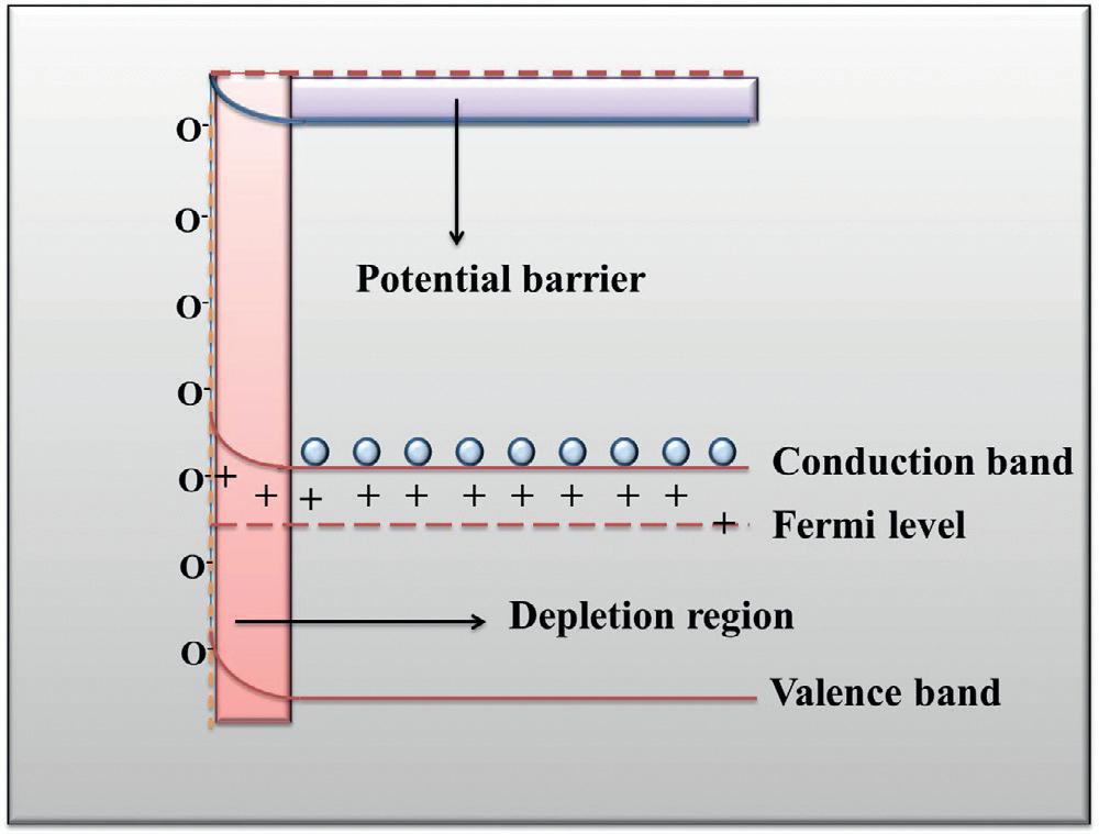
ThefundamentalprincipleofMOS–basedchemoresistivesensors isthechangeintheconductivityoftheMOSduetotheoxygenadsorptionanddesorptionreactionsonthemetaloxidesurface.Inthe caseofann-typeMOS-basedgassensorthesensingmechanismisas follows:inambientairatmosphere,oxygenadsorbedonthesurfaceof thesensinglayerbyextractingelectronsfromtheconductionbandof theMOS,whichresultsintheformationofaSchottkypotentialbarrier inMOS(Shankaretal.,2016).Theadsorptionofoxygenonthesurface ofMOSdependsontheoperatingtemperatureofthesensor.Atlower temperatures(<150°C),oxygenmoleculesareadsorbedintheformof molecularoxygenions(O2 )viathetrappingofacomparablyfewer numberofelectrons;however,athighertemperatures(>150°C),more electronsaretrappedbytheadsorbedoxygenandformatomicoxygen species(O andO2 )(Kashifetal.,2013).Theprocessesinvolvedin theadsorptionofoxygenonthemetaloxidesurfacecanbedescribed asfollows:
Theextractedelectronsfromthe conductionband(Ec )leavebehindpositivelychargedions,resultinginupward bandbendingandtheformationofan electron-depletionregionoraspacechargelayerintheMOS,asshownin Fig.1.1.Theheightanddepthofthe bandbendingdependontheamount andtypeofadsorbedoxygen.Dueto theformationoftheelectrondepletion region,anincreaseintheresistanceof theMOScanbeobserved.Whenthis surfaceisexposedtoreducinggases suchasacetoneandammonia,theadsorbedoxygenionsinteractwiththetargetgasesandthetrappedelectronsare releasedbackontotheMOSsurface.Theamountofoxygenremoved fromthesurfaceisproportionaltotheconcentrationofthereducing gas.Thustheheightanddepthofbandbendingandtheresistance oftheMOSdecrease(Ananya,2018; Shankaretal.,2016; Wangetal., 2010).TheoxygendesorptionfromtheMOSsurfaceinthepresenceof areducinggas(say,R)canbedescribedasfollows:
Figure1.1. Schematic representationofbandbending aftertheadsorptionofoxygen species(Priyaetal.,2021).
TheseelectronsarereleasedbackontotheMOSsurfaceandthe producedgasandwatermoleculearereleasedintotheatmosphere.On theotherhand,anoxidizinggasdepletesthechargecarriers,leadingto anincreaseinresistance.Similarly,inthecaseofp-typeMOS,where positiveholesarethemajoritychargecarriers,adecreaseintheresistanceisobservedinthepresenceofanoxidizinggasandanincrease intheresistanceinthecaseofareducinggas(Barsanetal.,2012; Neri, 2015; Subha&Jayaraj,2019). Table1.1 clearlysummarizestheresponse ofn-andp-typeMOStowardreducingandoxidizinggases.
1.2.2DesignofMOSgassensors
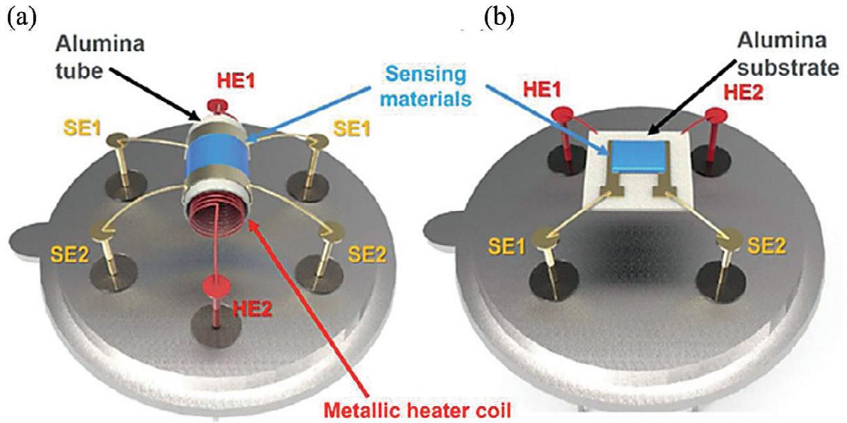
Thecommonlyavailableconfigurationsforthedesignof semiconductor-basedgassensorsare(1)sinteredpelletgassensors (Kazemietal.,2016),(2)thick-filmgassensors(Arshak&Gaidan, 2005),and(3)thin-filmgassensors(Mirzaeietal.,2019).The disadvantagewiththeuseofsinteredpelletgassensorsistheir relativelylowgasresponseduetothelimitedsurfacearea(Mirzaei etal.,2019).Thereforeresearchersaremoreinterestedintheuse ofthin-orthick-filmgassensorseitherinthetubularorplanar configuration,asshownin Fig.1.2.
Table1.1Changeintheresistanceofn-andp-typeMOSwhenexposed toreducingandoxidizinggases.
TypeofMOS
Whenexposedto reducinggases
Whenexposedto oxidizinggases
n-typeResistancedecreaseResistanceincrease p-typeResistanceincreaseResistancedecrease
Figure1.2. Schematicdiagram ofmetaloxidegassensor configurations:(A)tubularand (B)planar(SEandHErepresent thesensorelectrodeandheater electrode,respectively). Reproducedwithpermission from(Lee,2018),Copyright2018, Elsevier.
Thin-orthick-filmsensorsarepreparedbydepositingasensitive layeronaninsulatingsubstratesuchasalumina(Al2 O3 )andSi/SiO2 wafer.Themetaloxidepowderisgroundtogetherwithsuitablesolventslikeethanolandterpineolusinganagatemortartoformaslurry forthetubularconfiguration.Thentheslurryiscoatedonanalumina tube,onwhichapairofAuelectrodeshadbeenprintedpreviously, followedbydryingandsubsequentannealingathightemperatures. Finally,asmallNi–Cralloycoilisinsertedintothetubeasaheaterso astoadjustandoptimizetheworkingtemperatureofthegassensor.
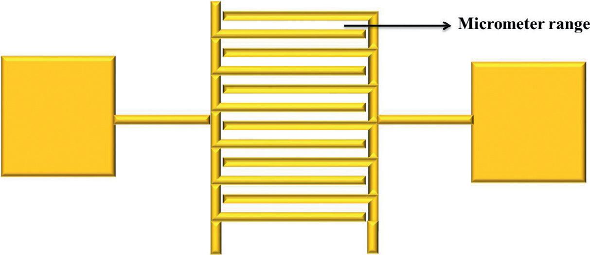
Thetubularconfigurationisshownin Fig.1.2A.Si/SiO2 oraluminasubstratewithpreprintedinterdigitatedgoldelectrodesiscommonlyused forthefabricationofplanarsensors(Fig.1.2B).Aschematicdiagram oftheinterdigitatedpatternisshownin Fig.1.3.Theuseofplatinum electrodesislimitedduetotheirhighcost.InsuchcasesAuelectrodes aremorepreferred.Theworkingtemperatureisobtainedbyplacing thedeviceontheexternalheaterorwiththehelpofaninternalheater printedatthebackofthesubstrate.Theplanarconfigurationismore
preferredforlarge-scaleproductionduetotheimprovedfabrication productivityandqualityofthesensor(Lee,2018; Mirzaeietal.,2019).
Whenweconsiderthesubstratematerial,aluminaisthebestavailablesubstratematerialduetoitshighthermalconductivityandstability,lowthermalexpansioncoefficients,highmechanicalstrength, andlowelectricalconductivity(Lee,2018).Thehighthermalstabilityof aluminaisanimportantfeaturesincemostMOS-basedsensorswork atrelativelyhighertemperatures.However,forthefabricationofelectrodesinthemicrometerrange(<10μm),microfabricationtechniques suchasUVorelectron-beamlithographyhastobeemployed,which leadstothepreferenceofaSi/SiO2 waferasthesubstratematerial overthealuminasubstrateduetothesurfaceroughnessofalumina substrate.
Plasticfoilscanalsobeusedassupportingmaterialsduetothe increasingdemandforflexiblegassensors.Theadvantagesofplastic foilsaretheirfoldableandwearabledesign,lightweight,transparency, andmassproductivityduetoroll-to-rollprintingprocesses.Polymers suchaspolyimide(PI),withrelativelyhighthermalstability,havebeen widelyusedassupportingmaterialsforflexiblesensorsoperatingata relativelyhighertemperature.However,theoperationofMOSsensors above400°CisdifficultusingPIsubstrates(Wangetal.,2016).
1.2.3Gassensingmeasurementsystem
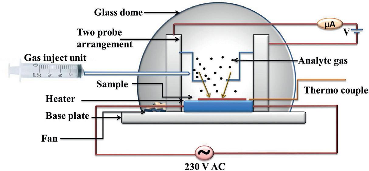
Generally,twotypesofmeasurementsystemsarecommonlyused forstudyingthegassensingpropertiesofthedevice:staticanddynamic. Fig.1.4 showstheschematicdiagramofastaticmeasurement system.Thesystemconsistsofatransparentgaschamberofadefined volumewithagasinlet.Thesampleisplacedinsidethechamberunder acontrolledtemperatureandhumidity.Theoperatingtemperatureof thesamplecanbeadjustedbyvaryingtheheatingvoltage.Duringthe measurement,afixedamountofanalytegasisinjectedthroughthegas
Figure1.3. Schematicdiagram oftheinterdigitatedelectrode pattern.
Figure1.4. Schematicdiagram ofthestaticgassensing measurementsystem(Mirzaei etal.,2018, 2019; Patil,2007).
Figure1.5. Schematicdiagram ofthedynamicgassensing measurementsystem.
inletwiththehelpofasyringe.Touniformizethedistributionofthe injectedtestgas,anelectricalfanisinstalledinsidethechamber.The concentrationofanalytegasiscalculatedwiththeratioofthevolumeof theinjectedgastothevolumeofairunderstandardatmosphericpressure.Afterreachingsaturationinthecurrent,thechamberisopened torecovertotheinitialcurrentintheairatmosphere.Theprocedure isrepeatedfordifferentanalytegasesatdifferentconditions(Mirzaei etal.,2018, 2019).
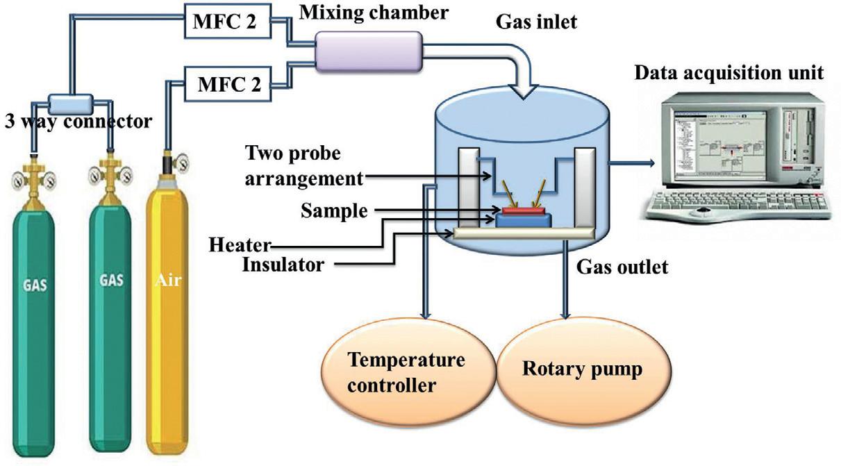
Adynamicsystemconsistsofgascylinderswithaknownconcentration,massflowcontrollers(MFCs),atestchamberwithagasinletandoutlet,heatingarrangement,electricalmeasurementarrangements,anddataacquisitionsystems,asshownin Fig.1.5.Withthe helpofMFCs,theflowrateofanalytegasesandsyntheticaircan becontrolled.Theconcentrationofanalytegasescanbechangedby mixingproperlywithsyntheticairornitrogeninamixingchamber connectedpriortothetestchamber.Thenthemixedvolumeofgas
ispassedintothetestchamberthrough thegasinlet.Thesampleisplacedon anexternalheaterandtheworkingtemperaturecanbecontrolledwithatemperaturecontroller.Thesampleisconnectedtoameasurementunittorecord thecurrentvariationcontinuously.Duringmeasurement,thecurrentthrough thesampleinairandinthepresence ofanalytegasatdifferenttemperatures isrecorded.Finally,afterthemeasurement,thegasfromthetestchamberis removedwiththehelpofarotarypump arrangement.
1.2.4Performanceparameters
Thegas-sensingperformanceofsensorsisevaluatedusingthefollowingimportantparameters(Balaguru2004; Tonezzeretal.,2015; Tshabalalaetal.,2016).
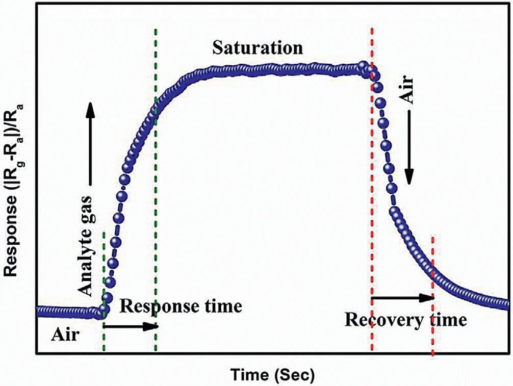
1.2.4.1Gasresponseandsensitivity
Generally,theresponseofasemiconductor-basedgassensoris definedasfollows: Response = Rg Ra Ra (1.6) where Ra and Rg representtheresistancesofthegassensorinthe presenceofairandtargetgas,respectively.Atypicalresponsecurve isshownin Fig.1.6.Sensitivityisthechangeinmeasuredresistance ( R)withachangeinanalyteconcentration( C),i.e.,theslopeofa calibrationgraph:S = S = R/ C .
1.2.4.2Selectivity
Itistheabilityofasensortodifferentiateaspecifictargetgasfrom amixtureofgases.Agoodsensorwilldetectaparticulargaswhile remaininginsensitivetoothergases.Theselectivitycoefficient(K)of agassensorcanbewrittenas K = SI SII (1.7) where SI and SII arethesensingresponsesofthesensortowardtwo differentgases,IandII,respectively.
1.2.4.3Stability
Stabilityisdefinedasthereproducibilityofthedeviceinthesensing measurementafterlonguse.Toavoidtheeffectsofnonrepeatability
Figure1.6. Typicalresponse curveofanMOS-basedgas sensor.