NanofabricationforSmartNanosensorApplications (MicroandNanoTechnologies)1stEditionKaushik Pal(Editor)
https://ebookmass.com/product/nanofabrication-for-smartnanosensor-applications-micro-and-nano-technologies-1stedition-kaushik-pal-editor/
Instant digital products (PDF, ePub, MOBI) ready for you
Download now and discover formats that fit your needs...
Nanovaccinology as Targeted Therapeutics Kaushik Pal
https://ebookmass.com/product/nanovaccinology-as-targetedtherapeutics-kaushik-pal/
ebookmass.com
Nickel-Titanium Smart Hybrid Materials: From Micro- to Nano-structured Alloys for Emerging Applications (Micro and Nano Technologies) 1st Edition Sabu Thomas (Editor)
https://ebookmass.com/product/nickel-titanium-smart-hybrid-materialsfrom-micro-to-nano-structured-alloys-for-emerging-applications-microand-nano-technologies-1st-edition-sabu-thomas-editor/
ebookmass.com
Nano-Optics: Fundamentals, Experimental Methods, and Applications (Micro and Nano Technologies) 1st Edition Sabu Thomas (Editor)
https://ebookmass.com/product/nano-optics-fundamentals-experimentalmethods-and-applications-micro-and-nano-technologies-1st-edition-sabuthomas-editor/
ebookmass.com
The Beautiful Little Things Melissa Hill
https://ebookmass.com/product/the-beautiful-little-things-melissahill/
ebookmass.com
Entrepreneurship in the Creative Industries. How Innovative Agents, Skills and Networks Interact Phillip Mcintyre
https://ebookmass.com/product/entrepreneurship-in-the-creativeindustries-how-innovative-agents-skills-and-networks-interact-phillipmcintyre/
ebookmass.com
Living Better Together: Social Relations and Economic Governance in the Work of Ostrom and Zelizer Stefanie Haeffele
https://ebookmass.com/product/living-better-together-social-relationsand-economic-governance-in-the-work-of-ostrom-and-zelizer-stefaniehaeffele/
ebookmass.com
Aid, Trade and Development : The Future of Globalization (Second Edition) Constantine Michalopoulos
https://ebookmass.com/product/aid-trade-and-development-the-future-ofglobalization-second-edition-constantine-michalopoulos/
ebookmass.com
Developments in the Formulation and Reinforcement of Concrete 2nd ed Edition Mindess
https://ebookmass.com/product/developments-in-the-formulation-andreinforcement-of-concrete-2nd-ed-edition-mindess/
ebookmass.com
A Christian Approach to Corporate Religious Liberty Edward A. David
https://ebookmass.com/product/a-christian-approach-to-corporatereligious-liberty-edward-a-david/
ebookmass.com
https://ebookmass.com/product/chemical-reactivity-in-confined-systemstheory-modelling-and-applications-pratim-kumar-chattaraj/
ebookmass.com
NanofabricationforSmart NanosensorApplications NanofabricationforSmart NanosensorApplications Editedby KaushikPal
InternationalandInterUniversityCentreforNanoscienceandNanotechnology(IIUCN), SchoolofEnergyMaterials,MahatmaGandhiUniversity,Kottayam,Kerala,India; WuhanUniversity,WuchangDistrict,Wuhan,HubeiProvince,RepublicofChina
FernandoGomes MacromoleculeInstituteProfessorEloisaMano;CivilEngineeringProgram,COPPE, TechnologyCenter-UniversityCity,FederalUniversityofRiodeJaneiro,RiodeJaneiro,Brazil
Elsevier
Radarweg29,POBox211,1000AEAmsterdam,Netherlands
TheBoulevard,LangfordLane,Kidlington,OxfordOX51GB,UnitedKingdom 50HampshireStreet,5thFloor,Cambridge,MA02139,UnitedStates
©2020ElsevierInc.Allrightsreserved.
Nopartofthispublicationmaybereproducedortransmittedinanyformorbyanymeans,electronicormechanical, includingphotocopying,recording,oranyinformationstorageandretrievalsystem,withoutpermissioninwritingfromthe publisher.Detailsonhowtoseekpermission,furtherinformationaboutthePublisher’spermissionspoliciesandour arrangementswithorganizationssuchastheCopyrightClearanceCenterandtheCopyrightLicensingAgency,canbefoundat ourwebsite: www.elsevier.com/permissions.
ThisbookandtheindividualcontributionscontainedinitareprotectedundercopyrightbythePublisher(otherthanasmay benotedherein).
Notices
Knowledgeandbestpracticeinthisfieldareconstantlychanging.Asnewresearchandexperiencebroadenour understanding,changesinresearchmethods,professionalpractices,ormedicaltreatmentmaybecomenecessary.
Practitionersandresearchersmustalwaysrelyontheirownexperienceandknowledgeinevaluatingandusingany information,methods,compounds,orexperimentsdescribedherein.Inusingsuchinformationormethodstheyshouldbe mindfuloftheirownsafetyandthesafetyofothers,includingpartiesforwhomtheyhaveaprofessionalresponsibility.
Tothefullestextentofthelaw,neitherthePublishernortheauthors,contributors,oreditors,assumeanyliabilityforany injuryand/ordamagetopersonsorpropertyasamatterofproductsliability,negligenceorotherwise,orfromanyuseor operationofanymethods,products,instructions,orideascontainedinthematerialherein.
LibraryofCongressCataloging-in-PublicationData
AcatalogrecordforthisbookisavailablefromtheLibraryofCongress
BritishLibraryCataloguing-in-PublicationData
AcataloguerecordforthisbookisavailablefromtheBritishLibrary
ISBN:978-0-12-820702-4
ForinformationonallElsevierpublications visitourwebsiteat https://www.elsevier.com/books-and-journals
Publisher: MatthewDeans
AcquisitionsEditor: SimonHolt
EditorialProjectManager: FernandaOliveira
ProductionProjectManager: PremKumarKaliamoorthi
CoverDesigner: GregHarris
TypesetbySPiGlobal,India
Contributors M.M.Abdullah PromisingCentreforSensorsandElectronicDevices(PCSED),Departmentof Physics,FacultyofScienceandArts,NajranUniversity,Najran,SaudiArabia
MostafaG.Aboelkheir MacromoleculeInstituteProfessorEloisaMano,TechnologyCenterUniversityCity,FederalUniversityofRiodeJaneiro,RiodeJaneiro,Brazil
GulzarAhmad DepartmentofPhysics,UniversityofAgriculture,Faisalabad,Pakistan
MazharS.AlZoubi DepartmentofBasicMedicalStudies,YarmoukUniversity,Irbid,Jordan
KhalidM.Al-Batanyeh DepartmentofBiologicalSciences,YarmoukUniversity,Irbid,Jordan
NormaAlias CenterforSustainableNanomaterials,IbnuSinaInstituteforScientificandIndustrial Research,UniversitiTeknologiMalaysia,Skudai,Malaysia
AlaaA.A.Aljabali DepartmentofPharmaceuticsandPharmaceuticalTechnology,Facultyof Pharmacy,YarmoukUniversity,Irbid,Jordan
LorcaAlzoubi DepartmentofPharmaceuticsandPharmaceuticalTechnology;MedicinalChemistry andPharmacognosyDepartment,FacultyofPharmacy,YarmoukUniversity,Irbid,Jordan
NidhiAsthana NationalCentreofExperimentalMineralogyandPetrology,UniversityofAllahabad, Allahabad,India
MurthyChavali ShreeVelagapudiRamaKrishnaMemorialCollege(PGStudies),Affiliatedto AcharyaNagarjunaUniversity,Nagaram;PGDepartmentofChemistry,DharmaAppaRaoCollege, AffiliatedtoKrishnaUniversity,Nuzvid;NTRC,MCETRC,Tenali,AndhraPradesh,India
RamchanderChepyala FPC@DCU – FraunhoferProjectCentreforEmbeddedBioanalytical SystemsatDublinCityUniversity,DublinCityUniversity,Dublin,Ireland
ShipluRoyChowdhury TissueEngineeringCentre,FacultyofMedicine,UniversitiKebangsaan Malaysia,KualaLumpur,Malaysia
Vı´torCorr^ eadaCosta MacromoleculeInstituteProfessorEloisaMano,TechnologyCenterUniversityCity,FederalUniversityofRiodeJaneiro,RiodeJaneiro,Brazil
MichaelK.Danquah ChemicalEngineeringDepartment,UniversityofTennessee,Chattanooga,TN, UnitedStates
KrishnaChitanyaEtika DepartmentofChemicalEngineering,BirlaInstituteofTechnologyand Science,Pilani,Rajasthan,India
IreneS.Fahim IndustrialEngineeringDepartment,SmartEngineeringSystemsResearchCenter (SESC),NileUniversity,Giza,Egypt
RomildoDiasToledoFilho CivilEngineeringProgram,COPPE,TechnologyCenter-University City,FederalUniversityofRiodeJaneiro,RiodeJaneiro,Brazil
SanjeevGautam NetajiSubhasUniversityofTechnology,Delhi,India
GaneshGollavelli CentreofExcellenceofNanotechnology;DepartmentofIndustrialChemistry, CollegeofAppliedSciences,AddisAbabaScienceandTechnologyUniversity,AddisAbaba,Ethiopia
HazidatulAkmaHamlan CenterforSustainableNanomaterials,IbnuSinaInstituteforScientificand IndustrialResearch,UniversitiTeknologiMalaysia,Skudai,Malaysia
AhmedM.Hassanein NanoelectronicsIntegratedSystemsCenter(NISC),NileUniversity,Giza, Egypt
MdEnamulHoque DepartmentofBiomedicalEngineering,MilitaryInstituteofScienceand Technology(MIST),Dhaka,Bangladesh
SaiqaIkram Bio/PolymerResearchLaboratory,DepartmentofChemistry,JamiaMilliaIslamia,New Delhi,India
PurnimaJain NetajiSubhasUniversityofTechnology,Delhi,India
YasirJaved DepartmentofPhysics,UniversityofAgriculture,Faisalabad,Pakistan
JaisonJeevanandam DepartmentofChemicalEngineering,CurtinUniversity,Miri,Sarawak, Malaysia
RocktotpalKonwarh DepartmentofBiotechnology,CollegeofBiologicalandChemical Engineering;CentreofExcellenceofNanotechnology,AddisAbabaScienceandTechnology University,AddisAbaba,Ethiopia
SamoKralj FacultyofNaturalSciencesandMathematics,UniversityofMaribor,Maribor,Slovenia
AmitKumar DyalSinghCollege,UniversityofDelhi,Delhi,India
EnamalaManojKumar BioserveBiotechnologies(India)PrivateLtd.,Hyderabad,Telangana,India
AhmedH.Madian NanoelectronicsIntegratedSystemsCenter(NISC),NileUniversity,Giza; RadiationEngineeringDepartment,NCRRT,EgyptianAtomicEnergyAuthority,Cairo,Egypt
TariqMahbub DepartmentofMechanicalEngineering,MilitaryInstituteofScienceand Technology,Dhaka,Bangladesh
ZaidBinMahbub DepartmentofMathematicsandPhysics,NorthSouthUniversity,Dhaka, Bangladesh
AhmedNawaz DepartmentofPhysics,UniversityofAgriculture,Faisalabad,Pakistan
SomiaNawaz DepartmentofPhysics,UniversityofAgriculture,Faisalabad,Pakistan
MohammadA.Obeid DepartmentofPharmaceuticsandPharmaceuticalTechnology,Facultyof Pharmacy,YarmoukUniversity,Irbid,Jordan
KaushikPal InternationalandInterUniversityCentreforNanoscienceandNanotechnology(IIUCN), SchoolofEnergyMaterials,MahatmaGandhiUniversity,Kottayam,Kerala,India;WuhanUniversity, WuchangDistrict,Wuhan,HubeiProvince,RepublicofChina
PeriasamyPalanisamy DepartmentofPhysics,GnanamaniCollegeofEngineering,Namakkal, TamilNadu,India
SureshBabuPalanisamy DepartmentofBiotechnology,CollegeofBiologicalandChemical Engineering,AddisAbabaScienceandTechnologyUniversity,AddisAbaba,Ethiopia
MamunRabbani DepartmentofBiomedicalPhysicsandTechnology,UniversityofDhaka,Dhaka, Bangladesh
LobnaA.Said NanoelectronicsIntegratedSystemsCenter(NISC),NileUniversity,Giza,Egypt
M.MunirSajid DepartmentofPhysics,GovernmentCollegeUniversity,Faisalabad,Pakistan
NaveedAkhtarShad DepartmentofPhysics,GovernmentCollegeUniversity,Faisalabad,Pakistan
BhashaSharma NetajiSubhasUniversityofTechnology,Delhi,India
ShreyaSharma NetajiSubhasUniversityofTechnology,Delhi,India
ZayedBinZakirShawon DepartmentofMathematicsandNaturalSciences,BRACUniversity, Dhaka,Bangladesh
ShashankShekhar NetajiSubhasUniversityofTechnology,Delhi,India
AsiyaS.I. BharathInstituteofHigherEducationandResearch(BIHER),BharathUniversity,Chennai, TamilNadu,India
PreetiSingh Bio/PolymerResearchLaboratory,DepartmentofChemistry,JamiaMilliaIslamia,New Delhi,India
FernandoGomes MacromoleculeInstituteProfessorEloisaMano;CivilEngineeringProgram, COPPE,TechnologyCenter-UniversityCity,FederalUniversityofRiodeJaneiro,RiodeJaneiro, Brazil
MurtazaM.Tambwala SAADCentreforPharmacyandDiabetes,SchoolofPharmacyand PharmaceuticalScienceUlsterUniversity,Coleraine,UnitedKingdom
SabuThomas InternationalandInterUniversityCentreforNanoscienceandNanotechnology (IIUCN),SchoolofChemicalSciences,MahatmaGandhiUniversity,Kottayam,Kerala,India
Editors’biography Professor(Dr.)KaushikPal isanIndiancitizen.Hedidhis PH.D.inPhysics(e.g.Nanotechnology,Multidisciplinary Sciences,AdvancedMaterialsScience,Spectroscopy)from UniversityofKalyani,West-Bengal,India.Mostrecentlyhe awardedwithhonorable DOCTOROFSCIENCE(D.SC.) from HigherNationalYouthSkillInstitute,Sepang, Selangor,Malaysia.Heisthe“DistinguishResearchProfessor” at FederalUniversityofRiodeJaneiro,Brazil andactingas “ChairProfessorandGroupLeader,(Chief-Scientist&Faculty Fellow)”positionin WuhanUniversity,WuchangDist.,Hubei Province,RepublicofChina.Mostrecently,hehasbeena visitingprofessorworkingandcontributingattheInternationalandInterUniversityCentrefor NanoscienceandNanotechnology(IIUCN),SchoolofEnergyMaterials,MahatmaGandhi University,Kottayam,Kerala.Heawardedinternationalprestigiousawardse.g.awardedthe Marie-CurieExperiencedResearcher(PostdoctoralFellow)bytheEuropeanCommission NetworkinGreece,andreceivedtheBrainKorea(BK-21)NationalResearchFoundation VisitingScientistFellowshipinSouthKorea.HewasappointedSeniorPostdoctoralFellowat WuhanUniversity,ChinaandwithinayearachievedtheprestigiouspositionofChief-Scientist andFaculty(CAS)FellowbytheChineseAcademyofScience.Heservedasresearchprofessor (GroupLeaderandIndependentScientist),atBharathUniversity(BIHER),Researchand Development,Chennai.Hiscurrentresearchspansarefocusingone.g.MolecularNanoscience andnanofabrication,functionalmaterials,condensedmatterphysics(expt.),CNTs/graphene, liquidcrystal,polymericnanocomposite,switchabledevice,electronmicroscopyand spectroscopy,bioinspiredmaterials,drugdelivery,integration,switchabledevicemodulation, stretchableelectronics,supercapacitors,optoelectronics,greenchemistry,andbiosensor applications.Hesupervisesasignificantnumberofbachelor’s,master’s,PhD,andpostdoctoral scholar’stheses,andhisresearchhasbeenpublishedinseveralinternationaltop-tierjournals frompublisherse.g.RoyalChemicalSociety,Elsevier,Springer,IEEE,andInTech.Hehas edited25bookchapterswithsignificantpublishers,contributed10reviewarticles,andhas editedseveralbooksforElsevier,AppleAcademicPress,andInTech.Dr.Palisanexpertgroup leaderandtheassociatememberofvariousscientificsocieties,organizations,andprofessional bodies.Inhisacademicandprofessionalresearch,hehasreceivedanumberofsignificant
awardsandprizes.Hehasbeenthechairpersonof30nationalandinternationalevents, symposia,conferences,andworkshops,andhascontributedto10plenary,28keynote,and30 invitedlecturesworldwide.
ProfessorFernandoGomes graduatedinchemistryfromthe FederalUniversityofEspı´ritoSanto(1999),andreceiveda MasterinEngineeringandMaterialsSciencefromtheState UniversityoftheNorthFluminenseDarcyRibeiro(2002),aPhD inScienceandTechnologyofPolymersfromtheFederal UniversityofRiodeJaneiro(2006),andapostdoctorateinthe chemicalengineeringprogramatCOPPE/UFRJ,Brazil.Heis currentlyAssociateProfessorattheMacromoleculesInstituteat UFRJ,CollaboratedProfessorattheCivilEngineeringProgram atCOPPE/UFRJandYoungScientistintheStateofRiode Janeiro(FAPERJ-2015).Hemainlyworkswithpolymeric nanocompositesobtainedfromrenewableresourcesinthree mainlines:(I)inthefieldofenvironmentalrecovery,coordinatingresearchprojectsfocusedon theuseofrenewableresourcesfortheremovalofoilinspills;(II)inthefieldofhumanhealth, coordinatingprojectsthatseekkineticandspatialcontrolofthedrugreleaseprocess;and(III)in thefieldofsensors,wherehecoordinatesprojectsthatseektoobtainplantfibersthatconduct electricityfortheiruseinsensorsforintelligentdevices.Supervisorof 103 undergraduate students; 28 M.Sc.students, 8 Ph.D.studentsand 5 PostDoc.NowadaysIamthesupervisorof 4 undergraduatestudents; 2 M.Sc.students, 14 Ph.D.studentsand 2 PostDoc.Memberofthe editorialboardofCurrentAppliedPolymerScience(ISSN2452-2716),AssociateEditorofthe MedCraveOnlineJournal(MOJ)PolymerScience(ISSN:2574-9773),andEditorofthe AcademicJournalofPolymerScience.HealsoawardedYoungScientistofRiodeJaneiroState (FAPERJ2011and2014),memberofPostGraduatePrograminScienceandTechnologyof PolymersoftheFederalUniversityofRiodeJaneirosince2008.
Introductiontonanomaterialsand nanomanufacturingfornanosensors TariqMahbuba,MdEnamulHoqueb
aDepartmentofMechanicalEngineering,MilitaryInstituteofScienceandTechnology, Dhaka,Bangladesh
bDepartmentofBiomedicalEngineering,MilitaryInstituteofScienceandTechnology(MIST), Dhaka,Bangladesh
1.1Nanosensors Sensorsaredevicesusedtodetectthepresenceofaspecificsubstanceortomeasureaphysical propertysuchastemperature,mass,orelectricaloropticalcharacteristicsandproducea signalforrecordingorfurtherpostprocessing.Thehistoryofsensorsisalongone.Thefirst thermostatcameintoexistenceinthe1880s,andthefirstinfraredsensorwasdevelopedin 1940.Nanosensorsaresimilartomacrolevelsensorsbuthaveatleastonedimensionin nanoscaleandcanbeusedtomeasuresignalsavailableatthatscale.Nanotechnology,withits rapiddevelopmentsinrecentyears,hasshowngreatpotentialinalmostallindustries. Variouselectronicsindustrieshavefueledthesedevelopmentstosatisfytheirneedfor miniaturization,andthenanosensorfieldhastakenadvantageoftheseadvancesforitsown development.Alargevolumeofresearchhasbeenconductedoverthelasttwodecadesin theareaofnanomaterialsforwiderapplications,includingnanosensors [1–10].Since nanosensorscandealwithsignalsproducedatthenanoscale,thesamplequantitiesneededare quitesmallanddetectionisveryrapid.Allofthesequalitieshavehelpedtheapplications ofvarioustypesofnanosensorsindifferentfields,especiallyinthemedicalandhomeland securityfields.Gainingaclearerunderstandingofthespecialpropertiesofferedatthe nanoscalebynanomaterials,evolutionofthevarioustechniquesfornanomaterialproduction, andexploitationofthespecialpropertiesofnanomaterialshavealladvancednanosensor development.
1.1.1Typesofnanosensors Duringtheshorthistoryofnanosensors,thistechnologyhasexperiencedsubstantial developments.Sinceavarietyofnanosensorsareavailabletoday,classificationcanbe somewhatdifficult.However,nanosensorscanbeclassifiedbasedontwogeneral factors:(1)structureand(2)application.
Basedonstructure,nanosensorscanbefurtherclassifiedintotwogroups: Opticalnanosensors: Opticalnanosensorsusethesensitivityoffluorescenceforqualitative andquantitativemeasurement.
Electrochemicalnanosensors: Thisclassofnanosensormainlydetectselectronicorchemical propertiesofarespectivesubstanceandtransducesasignal.Recently,majordevelopments havetakenplaceinthistypeofnanosensortechnology.
Basedonapplication,nanosensorscanbeclassifiedintochemicalnanosensors,nanoscale electrometers,nanobiosensors,deployablesensors,andsoon.
1.1.2Applicationsofnanosensors Nanosensorsaregraduallyassumingrolesinalmosteveryaspectofhumanlife.Anumberof sensorscandetectthepresenceofhazardousmaterialsormicroorganismsinfood,water,and air.Thesesensorsaresavinglivesindifferentcornersoftheworld.Inthemedicalfield nanosensorsarehavingahugeimpact:forexample,avarietyofnanosensorsarebeingusedin cancerdetection,DNAandproteindetection,andtargeteddrugdelivery.Deployablesensors havefoundapplicationsinhomelandsecurity.Variouschemicalsensorsarenowaddedto unmannedaerialvehiclestodetectthepresenceofpoisonousgasonthebattlefield,tosavethe livesofsoldiers.VarioustaggingsystemsemployRFIDchips,whicharealsoanapplicationof nanosensors.
1.2Nanomaterialsfornanosensors Forcenturiesthebeautyofthe400CELycurgusCupandthestrengthandbeautyofa Damascussteelbladehaveamazedpeople,butithasbeenonlydecadessincewediscoveredthe secretbehindtheseextraordinaryancientartifacts:nanomaterials [11,12].Nanomaterials aredefinedasthosenanoparticles(NPs)thathaveatleastonedimensioninnanometerscaleand thatexhibitsomespecialpropertythatisnotavailableinthebulkformofthesame material.Thoughunknowinglyusedinseveralancientartifacts,themodern-dayextensive research,informedfabrication,andutilizationofnanomaterialsbeganin1857,whenMichael Faradayreportedthesynthesisofso-called“activatedgold,”whichwasacolloidalsolution
ofAuNPs [13].Sincethattime,theuseofnanomaterialshasslowlybutsurelyspread, duetotheirextraordinarypropertiesassociatedwiththeirsize.Nanomaterialsshow extraordinarypropertiesdifferentthantheirbulksizebecauseoftheirnanoscaledimension. Thesurface-to-volumeratioofnanomaterialsisveryhigh,whichresultsinvariationsin chemical,mechanical,optical,andmagneticnature [14].Toexplorethepropertiesand applicationsofnanomaterialsproperly,itisjudicioustoclassifythem.However,severalfactors canbeconsideredinclassifyingnanomaterials,suchasphysicalandchemicalproperties, manufacturingprocess,dimensionality,uniformity,composition,andsoforth [15].Fromthe pointofviewofthischapter,weclassifynanomaterialsintofourclassesbasedontheir chemicalcomposition:(1)carbon-based,(2)organic-based,(3)inorganic-based,and(4) composite-basednanomaterials.Inthefollowingsections,wediscussdifferentnanomaterials thatfallwithinthesefourcategoriesandtheirapplications,especiallyasnanosensors.
Atthispoint,abriefintroductiontonanosensorsmaybeveryhelpfulforthosenewtothis field.Asensorisadevicethatdetectsandrespondstoanychangeinitsenvironment. Dailylifeisfullofsensors,suchaslightsensors,rainsensors,laneassistinautomobiles, smokeandfirealarmsensors,electricalsensors,andsoforth.Na nosensorsperformthe samefunction,butonamuchsmallerscale(1– 100nm),capableofsensingpathogens, viruses,molecules,orevenasinglechemicalelement.Themainadvantagesofnanosensors aretheminutesamplequantitiesrequired, speed,portability,andlowcostinmass production,amongothers.
Thehistoryofnanosensorsisonlydecadesold.Sincethebeginningofthecurrentcentury,the worldhasexperiencedarapidescalationofproductionanduseofnanosensorsasaconsequence oftwofactors.First,nanosensors,duetotheirexcellentperformance,haveconvincedthe worldthattheycanbesuccessfullyusedindifferentapplicationsvaryingfromthefood industry,fireandhazardousgasdetection,tovariouscriticalfieldslikemilitaryandadvanced medicalapplications.Secondly,thereisatremendousadvancementofdifferent manufacturingprocessesusedformanufacturingnanosensors,increasedavailability,and developmentofnewnanomaterialsandmoreclearunderstandingofnanoscale phenomena [16].
1.2.1Propertiesofnanomaterialsfornanosensors Nanomaterials,duetohighsurface-to-volumeratioandthemanufacturingprocess,offersome extraordinarypropertiesthatcanbeexploredtoproducevariousapplicationsindrug manufacturing,environmentalsensingandprotection,materialsandmanufacturingindustries, electronics,energyharvesting,etc.Afewpropertiesthatarerelevanttonanosensorsarebriefly describedinthefollowingsections.
1.2.1.1Opticalproperties
Nanomaterialsoffersomeexcellentopticalproperties,suchaslightabsorption,color,light emission,andmagnetoopticalpropertiesduetotheirsizes;thesepropertiesarequitedifferent fromtheirbulkpropertiesandmakenanomaterialsagoodchoiceforopticalnanosensors.One ofthefirstnanosensorsdevisedtomeasureinhomogeneouspHdistributioninthreedimensionalresolutionwasfluorescein-based,usingapolyacrylamidenanoparticle incorporatedwithpH-sensitivefluorescein-acrylamide [17].Fluorescentnanosensorscan respondtosomespecificstimuliprovidedbythesurroundingenvironmentandtransducea fluorescencesignaltothedetectortosenseenvironmentalchanges.Thesenanosensorsareused tomakeoxygensensors [18] andtemperaturesensors.Thelocalizedsurfaceplasmon(LSP) effectofthenoblemetalnanoparticleisacurrentactivefieldofresearchformaking nanosensors(Fig.1.1).Whenananoparticleconfinessurfaceplasmon,duetoitsdimension, comparabletothewavelengthoflight,thefreeelectronofthenanoparticleparticipatesin thecollectiveoscillation.Thisphenomenoniscalledlocalizedsurfaceplasmon(LSP) [19]. TheLSPeffectgreatlyenhancestheelectricfieldnearthenanoparticlesurfaceandatthe plasmonresonantfrequencytheparticleshowsmaximumopticalextinction.Anumberofgas sensors [20,21] andpHsensors [22,23] aremanufacturedusingLSP.
1.2.1.2Electronicproperties Nanomaterialscanofferquiteexceptionalelectronicpropertiesthatoriginatefromtheshape andstructureofthenanomaterial.Whentalkingaboutexceptionalelectronicproperties,the namethatcomestomindfirstisgraphene.Graphenehasasingle-layer2Dhoneycomb structureinwhichbothsurfacesareavailableformoleculeabsorption.Thestructurecausesthe electronseemlytobemassless [24] andtheelectronmovesatanaveragespeedwhichis 300timeslessthanthespeedoflightatvacuum.Thisallowsmanyrelativisticeventstobe
Schematicdiagramoflocalizedsurfaceplasmoneffect.
observablewithoutaparticleaccelerator [15].Thecarbonnanotube(CNT)inwhichgraphene actsasabuildingblockalsoofferssomeexcellentelectronicproperties.The sp 2 hybridization ofthecarbonorbitalsintheCNTleavesfreeelectronsatthesurfaceofthetubes,which yieldstheseexcellentproperties.CNTcanshowmetallic,semiconducting,orinsulating behavior,whichcanbecontrolledbycontrollingthediameter,chiralityoftheCNT,andany functionalizationordopingdoneonCNT [25].Nanosensorsusingthesepropertiesdetectusing twomethods:(a)currentenhancement,and(b)currentinhibition.Variouselectrochemical sensorshavebeendevelopedfordifferentpurposes,suchasdetectingdopamine [26],histamine [27],bacteria [28],glucose [29],andsoforth,usingtheelectronicpropertiesofnanomaterials.
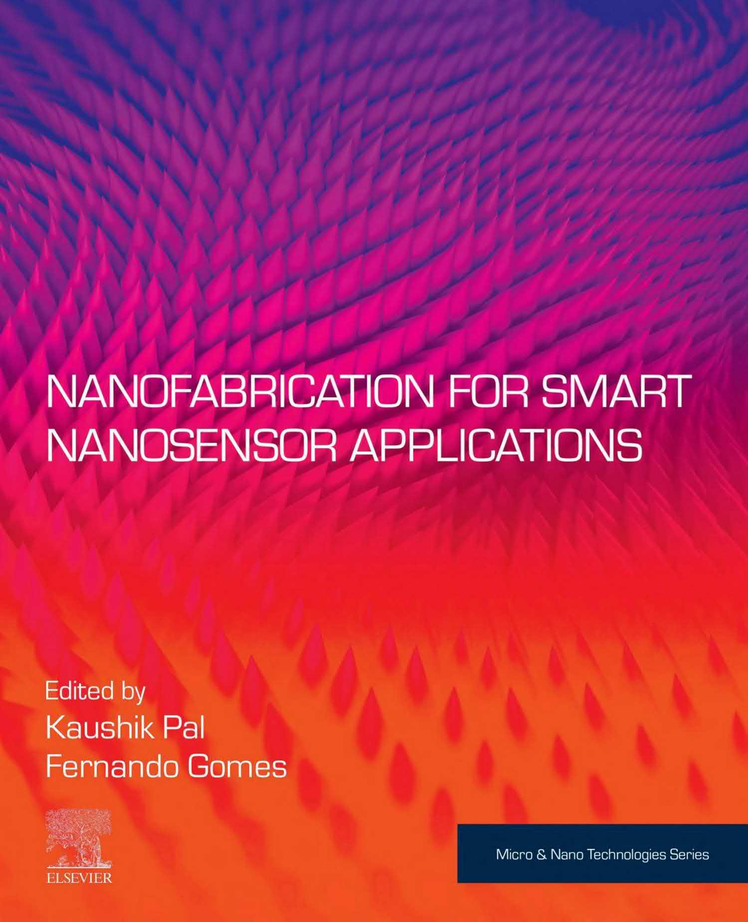
1.2.1.3Magneticproperties Duetotheunevenarrangementandorientationofelectronsinnanomaterials,andtheirsize, nanomaterialsexhibitexcellentmagneticpropertiestoo.Magneticpropertiesofnanomaterials arebecomingacenterofinterestindifferentbranchesofengineering,includingbutnotlimited todifferenttypesofcatalysis,biomedicineforcancertreatment,magneticfluids,nuclear magneticresonanceimaging(NMR),magneticresonanceimaging(MRI),andenvironmental remediation [30].Magneticnanosensorsusedifferenttechniquestoperformdetection,likethe effectmagneticparticlesexertonwaterprotonrelaxationrates,bydeterminingtherelaxation ofthemagneticmomentwithinthemagneticparticle,bydetectingthepresenceofamagnetic particleusingmagnetoresistivity,etc.Kohetal.explaindifferentbiosensorsusingthe previouslymentionedmethods.Thefollowingfiguresshowschematicrepresentationsofthe threeprocedures [31]. Fig.1.2Arepresentshowmagneticnanoparticlesdephasetheprotonsof waterforabetterMRIscan.Magneticparticlesgenerallystaydispersedinaliquidsolvent.But whenatargetanalyte(trianglein Fig.1.2A)appears,thedispersednanoparticlesproducean aggregatearounditandeventuallythisaggregatedephasesthespinsofwaterprotonsmore efficientlythanthedispersedstate.Thisreducesthespin-spinrelaxationtimeT2 toproducea betterMRIimage. Fig.1.2Bshowstheapplicationofmagneticmomentrelaxationwithina magneticnanoparticleforbacterialdetection.ThetypeofrelaxationusedhereisNeel relaxation.IntheupperfigureA,amagneticfieldisappliedtothenanoparticlesandtheyorient themselvesalongtheappliedfield.Someofthenanoparticlesarebondedwiththetarget bacteria.Later,infigureB,thefieldisremovedandmanyoftheparticlesexperienceBrownian relaxationandrandomlyorientinadifferentdirection.Butthenanoparticlesbondedtothe bacteriacannotundergoBrownianrelaxationandrathershowNeelrelaxation,whichis comparativelysloweranddetectable.Thesuperconductingquantuminterferencedevices (SQUIDs)detecttheslowerNeelrelaxationandbacterialdetectionisperformed. Fig.1.2C showstheoperationofamagnetoresistivesensor.Thebasicprinciplethatamagnetoresistive sensorappliesisthatthemagneticparticlebondstothesurfaceofthesensorandeventually altersitsmagneticfield.Thiscausesachangeinsensorcurrentandthedetectionisperformed. Therearetwomechanismsthroughwhichmagneticparticlesbindtothesensorsurface:(i)direct labeling,and(ii)indirectlabeling.Inthecaseofdirectlabeling,magneticnanoparticlesdirectly
Sensor functionalization
antibody BSA
Linker incubation
Analyte incubation
Nanotag-based quantification
Capture antibodyBSAAnalyteBiotinylated antibody
Streptavidin-coated magnetic nanotag
Magnetoresistive Sensor
(A)Magneticpropertyofnanomaterialsusedforsensingapplications [31].(B)Magneticpropertyofnanomaterialsusedforsensing applications(workingprincipleofSQUID) [31].(C)Schematicdiagramofgiantmagnetoresistivesensorapplication [31].
Fig.1.2
bindtothesurfacefunctionality,whileforindirectlabelingasandwichassayiscreated. Fig.1.2C schematicallyshowsthedetectionofproteinbycreatingasandwichassay.
Nanoparticlespossessmanymoreextraordinarypropertiesincludingmechanicalandthermal properties,butthesepropertiesarenotveryimportanttothecurrentsubjectpointofview.
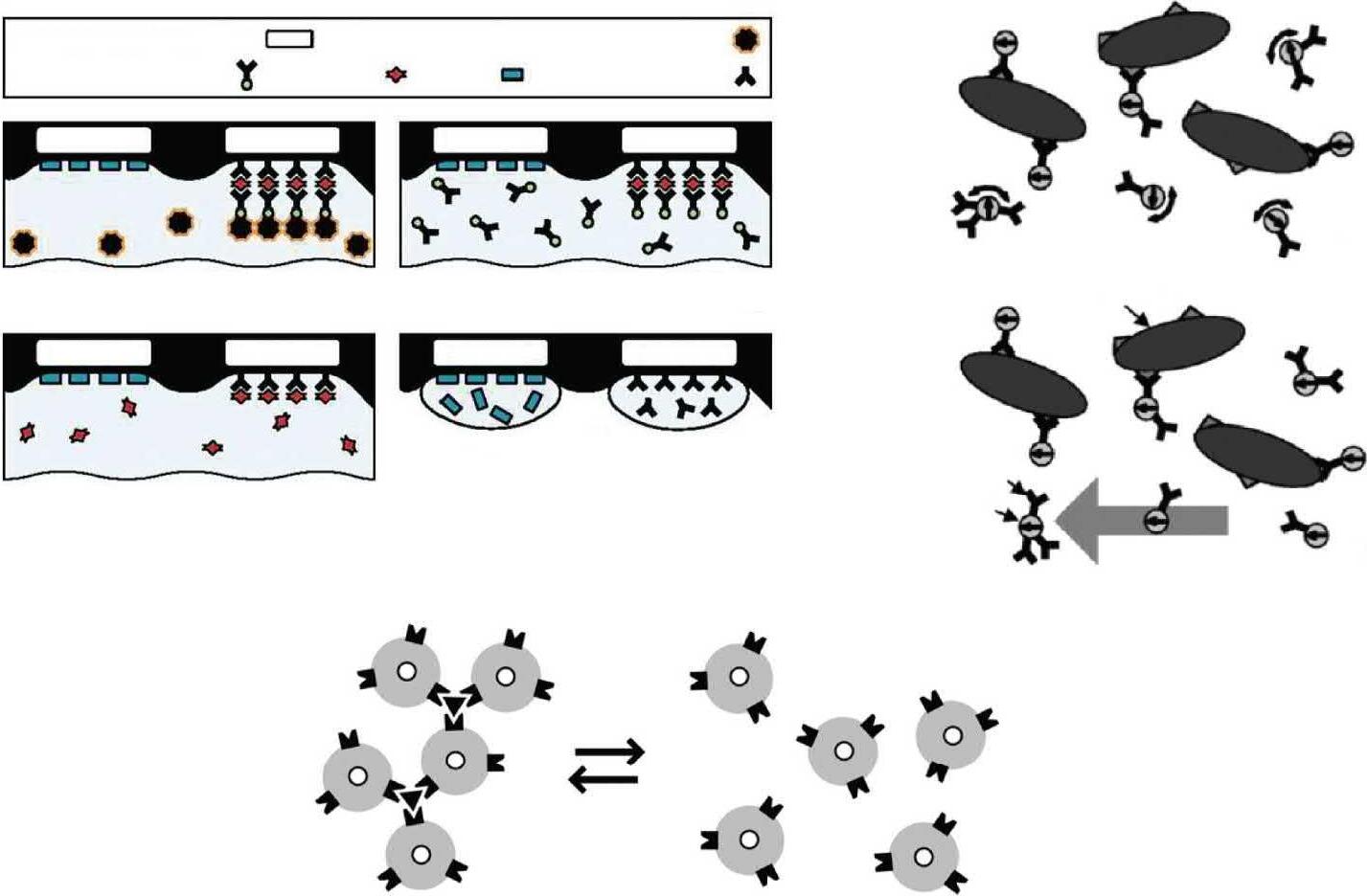
1.2.2Differentnanomaterialsfornanosensors Todiscussandunderstandtheuseofnanomaterialsindevelopingnanosensors,itishelpfulto classifythemintodifferentgroups.Butclassifyingnanomaterialsintodifferentgroupsisa formidablejob.Nanomaterialscanbepreparedusinganumberofbottom-upprocessessuchas cutting,ballmilling,extruding,chipping,pounding,andmanymore [32] andtop-down approaches [33] resultingindifferenttypesofstructures,withdifferentsurfacecoatings,which cancausetheclassificationtobeobscure.Forthatreason,herewedonotputtoomuch concentrationonclassifyingnanomaterials,butratherweshedsomelightonsomecommonly usednanomaterials.Aschematicrepresentationofcarbon-basednanomaterialsisprovidedin Fig.1.3 forabetterunderstandingofthediversenatureofnanomaterials.
Fig.1.3
Differentcarbon-basednanomaterials [34]
1.2.2.1Carbonnanotube Firstdevelopedin1991byIijima,thecarbonnanotube(CNT)isbyfarthemost-usedcarbonbasednanomaterial.Itisacylinderhavingdiametersfromfractionstotensofnanometersanda lengthuptoseveralmicrometers.Thereexistbothsingle-walled(SWCNTs)andmultiwalled (MWCNTs)nanotubesthatareformedbysingleandmultiplelayersofgraphenelamella, respectively,seamlesslyrolledup [14].TheCNTiscommonlyproducedbyachemicalvapor deposition(CVD)techniqueorvaporizationofgraphiteinafurnaceinaninert(argongas) atmosphere.TheCNTpossessessomeexcellentproperties,suchashighstrengthcausedbyits hexagonalstructure,exceptionalelectronicpropertiescausedbythefreeelectronavailable after sp 2 hybridization,andeaseoffunctionalizationwithdifferentorganicmoleculesthat provideameanstointeractselectivelywithdifferentanalytes.Thiseasy-to-functionalize propertyenablesCNTstobeusedasprobetipsforawiderangeofchemicalandbiological applications.
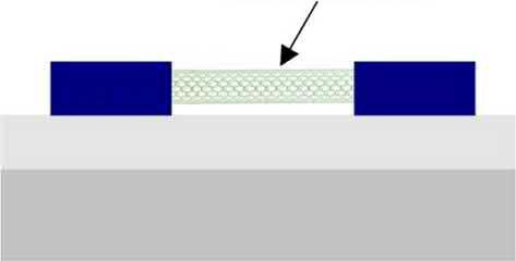
ThemainapplicationoftheCNTasasensorisinthefield-effecttransistor(FET).Though theCNTisrobustandinertinnature,itishighlysensitivetochemicaldoping.Awidevarietyof FETsaremanufacturedbychemicaldopingofCNTs. Fig.1.4 showsaschematicdiagram ofCNT-FET.
CNT-FETsareusedtodetectdifferenttypesofgaseslikeCO2,NH3,O2 [35],NO2,N2 [36],and soforth.CNT-FETsarealsousedfordetectioninbiologicalscience.Avarietyofsensors havealreadybeendevelopedbyresearchersfordetectingproteins [37],enzymes,and β-D glucose [38],amongothers.
1.2.2.2Nanowires Nanowiresarealsocommonlyusedinmakingnanosensors,justlikeCNTs.Nanowiresare producedthroughavarietyofprocessessuchaschemicalvapordeposition(CVD),laser ablation,alternatingcurrentelectrodeposition,andthermalevaporation [25].Nanowirescanbe madeupofdifferentmaterialsbutsiliconenanowireshavedrawnrecentinterest.Theelectrical propertiesandsensitivityofsiliconnanowirescanbetunedproperlyandreproduciblyby
Fig.1.4 SchematicdiagramofCNT-FET
Fig.1.5
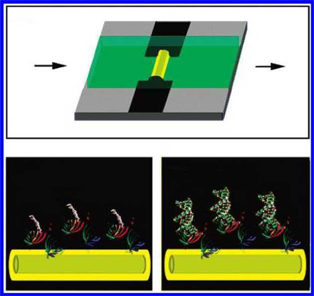
(A)SchematicofasensordeviceconsistingofaSiNW(yellow)andamicrofluidicchannel(green), wherethe arrows indicatethedirectionofsampleflow.(B)TheSiNWsurfacewithPNAreceptor. (C)PNA-DNAduplexformation [40].
controllingthenanowirediameteranddopantconcentration [39].Hahmetal.produceda SiNW-basedsensortodetectDNAandDNAmismatches [40] inwhichthesiliconnanowire devicesweremodifiedwithpeptidenucleicacidreceptors.Thegoldnanoclustercatalyzed chemicalvapordepositiontechniquewasemployedtopreparethenanowiresusedinthis sensor.Thenanowireswereassembledonthesensoralongwithpeptidenucleicacid. Aschematicdiagramofthedeviceisgivenin Fig.1.5[40].WhenawildtypeormutantDNAis introducedtothesensorviathemicrofluidicchannel,peptidenucleicacidbindswiththeDNA andcreatesatinychangeoftheconductanceofthesiliconnanowire.Thischangeof conductanceenablesthesensortodifferentiatebetweenfullycomplementaryor mismatchedDNA.
NanowiresarealsousedtomakegassensorsthatcanqualitativelydetectNH3.
1.2.2.3Nanoparticles Nanoparticlesareacommonlyusednanomaterialnotonlyinsensormanufacturingbutalsoin manyotherengineeringapplications.Althoughthenamesuggestsananoparticleisasingle molecule,NPsarenotjustsimplyonemoleculebutratheracombinationofthreelayers.These layersare(a)thesurfacelayer,whichcanbeusedtofunctionalizethenanoparticle;(b)theshell layer;and(c)thecore,whichisessentiallythecentralportionoftheNP [41].Nanoparticlesare
preparedusingvariousapproacheslikebottom-upsynthesis,includingbutnotlimitedto chemicalvapordeposition(CVD),spinning,plasmasprayingsynthesis,andlaserpyrolysis, andtop-downapproaches,includingbutnotlimitedtomechanicalmilling,sputtering,andlaser ablation.Nanoparticlescanbeclassifiedintovariousclasses,forexample(a)carbon-based nanoparticle,(b)metalnanoparticle,(c)ceramicnanoparticle,(d)semiconductornanoparticle, and(e)polymernanoparticle. Fig.1.6 showstheSEMandTEMimagesofdifferent nanoparticles(NPs).Nanoparticlesofferexceptionalelectronic,optical,magnetic,mechanical, andthermalproperties.Amongthese,thefirstthreepropertiesareexploitedtoproducemany sensors.Metallicnanoparticlesareusedtoenhancesurfaceplasmonresonancesensitivity.The surfaceplasmonresonancetechniqueisusedinmanyopticalsensorsdescribedintheprevious section.Palladiumnanoparticlesdepositedonetchedporoussiliconareusedtodetecthydrogen intheenvironment,whilecarbonelectrodeswithdepositedgoldnanoparticlesareusedto detectcopperinwater [16].
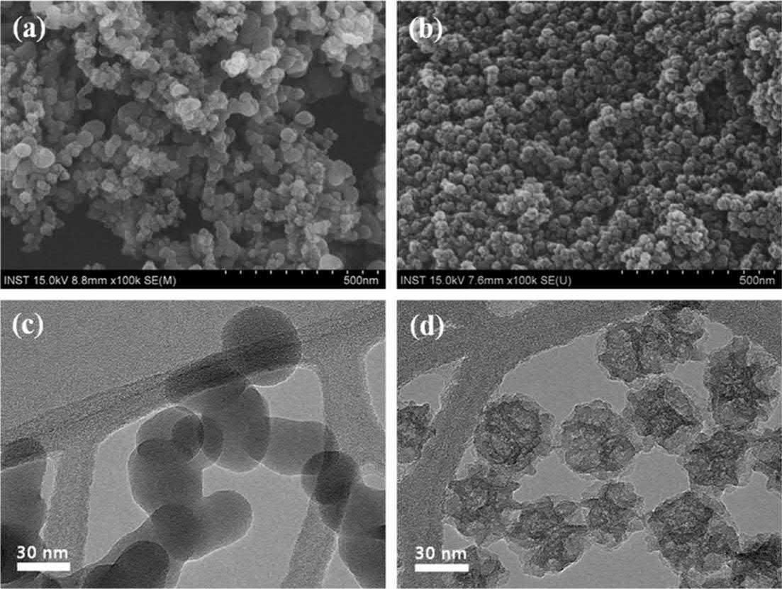
Fig.1.6
SEMimageof(A)nonporousMA-SiO2 NPs,(B)mesoporousMA-SiO2 NPs.TEMimagesof (C)nonporousMASiO2 NPsand(D)mesoporousMA-SiO2 NPs [18]
Introductiontonanomaterialsandnanomanufacturingfornanosensors11
1.2.2.4Fullerenes
Duetotheiruniqueproperties,fullerenesarenowreceivingmajorattentionfromthescientific community.Fullereneshaveahexagonalgroundstatewith sp 2 hybridizationandarehighly symmetricwith120symmetryoperations.Fullerenesareverystrongandbouncebacktotheir initialshapeafterdeformation [15].Amongotherproperties,fullereneshavehighsurface-tovolumeratio,highelectronaffinity,andahydrophobicsurface.Agoodnumberofsensorshave beendevelopedusingfullerenesalongwithothernanomaterialstoformnanocomposites. Brahmanetal.developedaC60-MWCNTnanosensorfordetectingpyruvicacid [42].Another electrochemicalsensorwasdevelopedbythesameresearcherthatusesafullerene,copper nanoparticle-fullerene,MWCNTcompositetodetectparacetamol [43].Heretheyuseda pretreatedcarbonpasteelectrode(CPE)onwhichfullerene-C60andmultiwalledcarbon nanotubes(MWCNTs)weredroppedtoproduceamodifiedCPE.Latercoppernanoparticles (CuNPs)weredepositedelectrochemicallyonthemodifiedCPEandananocompositefilmof CuNPs/C60-MWCNTs/CPEwasformed.Thiscompositeshowedexcellentperformancein paracetamolrecognitionanddetermination.
1.3Nanomanufacturing Nanomanufacturingistheprocessofmanufacturingnanomaterialsorvariousstructuresin nanoscalefordifferentapplications.Thiscanbeconsideredanupdatedversionof micromanufacturing/microfabricationinwhichthedimensionatwhichthemanufacturingisdone isseveralorderssmaller.Theterm nanofabrication issometimesusedasanalogousto nanomanufacturing,butsometimesnanofabricationrefersmoretoananoscalefabricationprocess thatisusedinfundedresearchworkandnanomanufacturingisusedtorefertomanufacturing productsforrevenuegeneration [44].However,inthischapter,wearenotveryconcernedaboutthe lackofaspecificdefinitionforthetermnanomanufacturing;rather,weprovideageneralideaof currentprevailingnanomanufacturingprocessesformanufacturingnanosensors.
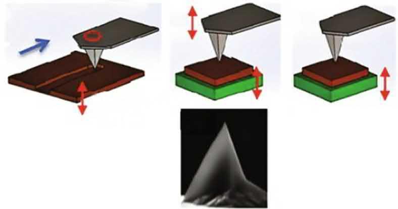
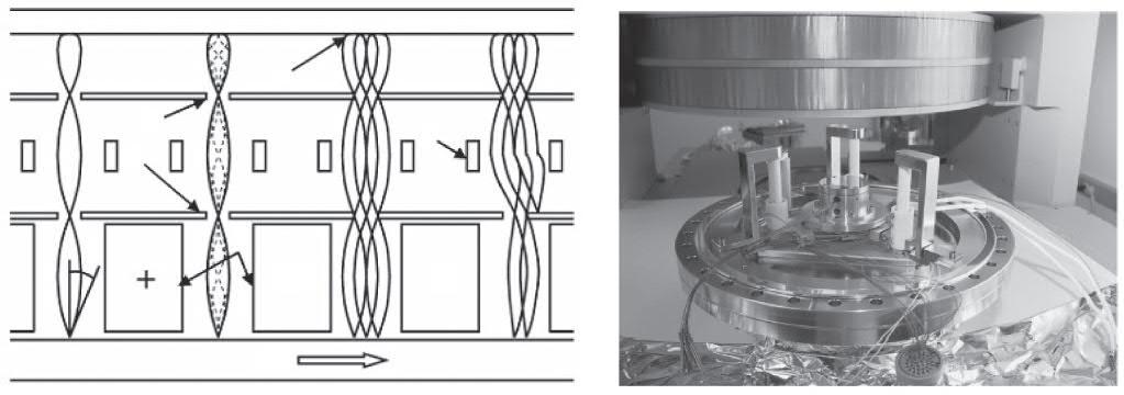
Aschematicdiagramofanultrasonicassistednanomanufacturingprocessisshownin Fig.1.7 Inthefigure,variouspossibletypesofvibrationconfigurationsareshownforthemachining process.Theresearchgroupreportedthatthismethodcanbesuccessfullyappliedtoproduce 3Dnanoobjectsofdiscreteheightlevelsandalsoofcontinuouslyvaryingheight [45].
1.3.1Nanomanufacturingprocesses Themaindrivebehindthenanomanufacturingprocessistheever-increasinghungerofthe electronicsindustrytoobtainsmallersizes.Currently,amicrochipthatwecanholdonour fingertipscanstoregigabytesofdata.Tosatiatethishunger,differenttypesof nanomanufacturingprocesseshavebeendevelopedthatcanbeclassifiedintothreebroad
(A)UltrasonicassistedAFM-basednanomanufacturingprocess.(B)Low-frequencytip-sample interacting.(C)Ultrasonictip-sampleinteractionwhilethetipisstationary.(D)SEMimageofAFM tip [45].
approaches:(1)top-downapproach,(2)bottom-upapproach,and(3)molecularassembly. Thesethreeapproachesarebrieflydescribedinthefollowingsections.
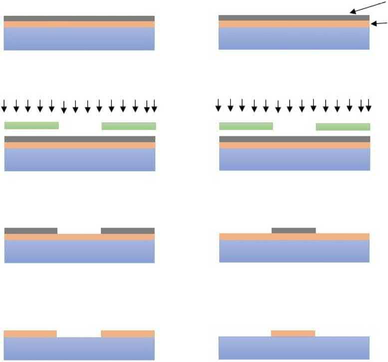
1.3.1.1Top-downapproach David,thefamousstatuecreatedbyMichelangelo,isoneofthemostnotablesculpturesofall time.However,ifsomeoneaskshowDavidoranyotherstoneorwoodensculptureismade,the answerissimple:alargeblockofstoneorwoodisgraduallytrimmedtothefinalshape.Thisis atop-downapproach.Innanomanufacturing,thisapproachisusedwhenalargeblockof materialistakenand,bymachining,thematerialisremovedlittlebylittletillthefinalshapeis obtained.Thetop-downapproachconsistsoftwosteps:(1)nanolithographyand(2)transferof pattern.
Innanolithography,thedesiredpatterniscreatedonaspecialtypeofsacrificiallayercalleda resist.Thereareanumberofnanolithographytechniques,suchasphotolithography, electronbeamlithography,X-raylithography,softlithography,andsoforth.Thebasicideain everycaseissimilar.First,alayerofresistisappliedtothesubstrate.Thenwiththehelp ofapatternthephotoresistisexposedtoanenergysource:forexample,photolithographyuses ultravioletrayswhileelectronbeamlithographyusesanelectronbeamandX-ray lithographyusesanX-ray.Duetothispatternedexposure,theresistundergoesachemical processandthechemicalandmechanicalpropertiesvarythroughoutthewholecoating. Later,somepartoftheresist(exposedorunexposedpart)isremoved,dependingonthe positiveornegativeresist,andapatterniscreated.Nowthemetallayer(SiO2 in Fig.1.8) isreadyfortheetchingprocess.Afteretchingthepatterncreatedbytheresistisremoved mechanicallyorchemically.Thesimplifiedprocessisgraphicallyrepresentedin Fig.1.8.
Fig.1.7
Photoresist
SiO2 layer
Pattern/Mask
Development before Etching
Etching and stripping of photoresist
ImageofpositiveandnegativeresistinX-raylithography.
Currently,thetop-downapproachprevailsasthemostpopularandwidelyusedapproachinthe nanomanufacturingindustry.Buttheothertwoapproachesarealsobeginningtohavetheirown positionsinnanomanufacturing.
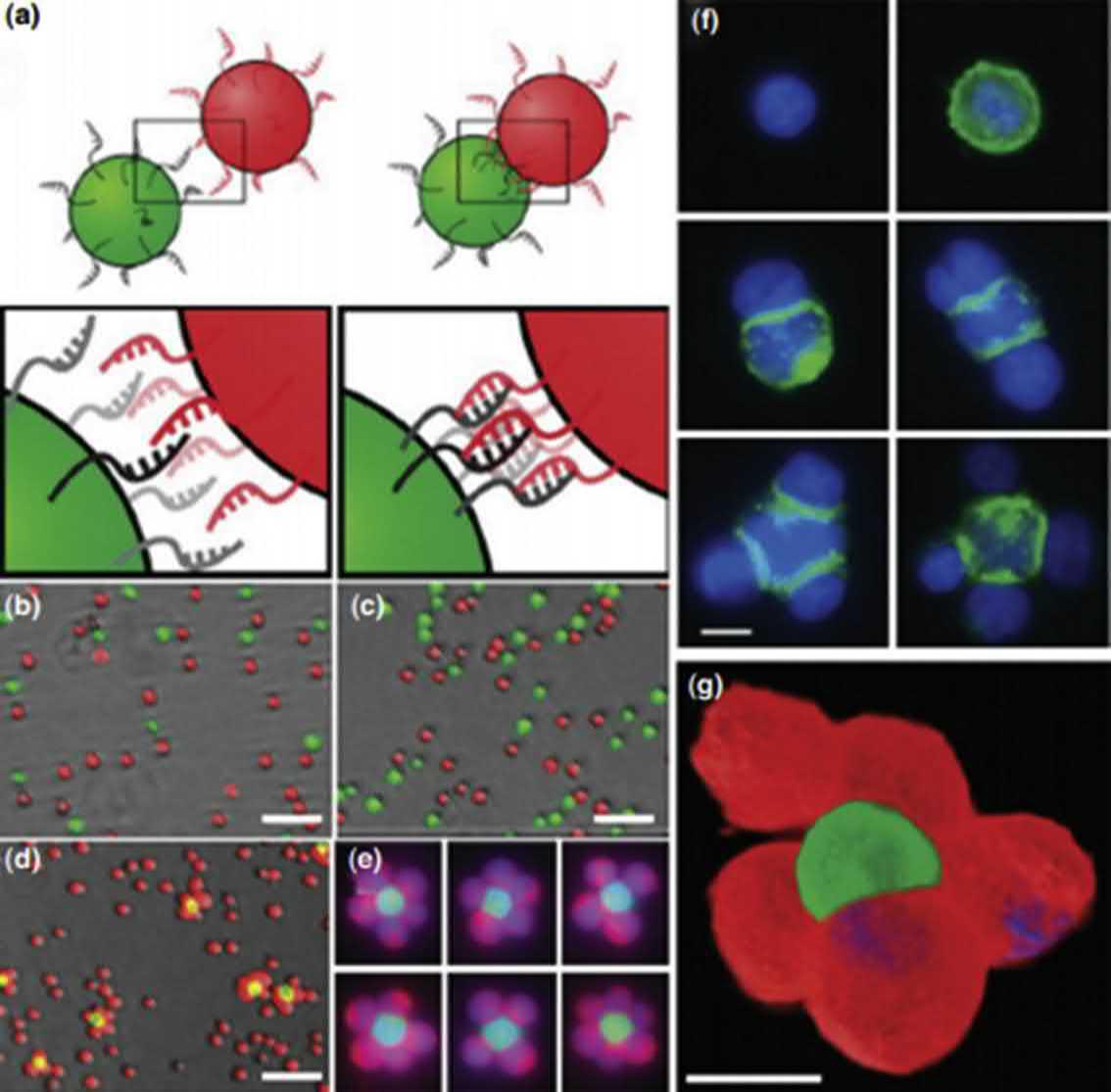
1.3.1.2Bottom-upapproach Thebottom-upapproachissimilartobuildingupahousebrickbybrick(Fig.1.9).Inthis approach,thefinalstructureisdevelopedbyassemblingorjoiningsmallcomponents,even molecules.Typicallythereareseveralbottom-upapproaches,includingphysicalorchemical vapordeposition,contactprinting,imprinting,assemblyandjoining,andcoating.Thebottomupapproachhashighpotentialinhealthcareandmedicalapplications.Carbonnanomaterials andcarbonnanotubescanbeusedforabottom-upapproachandadevicethatcanworkonan individualcellcanbenanofabricatedusingthisapproach(Fig.1.9).
1.3.1.3Molecularself-assembly Molecularself-assemblyisthenewestapproach,inwhichthecomponents,especially molecules,assemblethemselvesinthedesiredfashiontoproduceananoobjectwithoutthe directionofanoutsideforce.Thisprocessinvolvesdifferentpropertiessuchasshape,surface
Fig.1.8
Fig.1.9
Bottom-upapproachusedintissueengineering.(A)Complementaryoligonucleotideswerecovalently coupledtothesurfacesofdifferentcellsbyclickchemistry.(B–E)Twononadherentcelltypeswere mixed,anddidnotaggregateiftheirsurfacesweremodifiedwith:(B)nooligonucleotides, (C)noncomplementaryoligonulceotides.However,specificaggregationwasobservedifthecell surfacesweremodifiedwithcomplementaryoligonucleotides(D,E).(F)AggregationofDAPIstained cells(blue),withthecentralcellmodifiedwithfluorescein-conjugatedoligonucleotides(green).(G)3D reconstructionofanaggregateofTexasRed-labeled(red)andfluorescein-labeledcells(green) [46].
properties,charge,polarizability,andmagneticdipoleofthemoleculetodrivethemto assembletogethertoformaparticularstructure.Thisisstillagrowingfieldandvarious developmentsarerequiredbeforethisapproachisusedinindustry.
Introductiontonanomaterialsandnanomanufacturingfornanosensors15
1.4Nanomanufacturingprocessesfornanosensors Nanomanufacturingcanbedefinedastheabilitytomeasure,predict,andmanufactureon atomicandmolecularscalesandtoexploittheuniquepropertiesshownbynanomaterialsatthat scale.Nanomanufacturingisamultidisciplinaryfieldandresearchersfromvarious backgroundsarecontributingtoit. Fig.1.10 showsgraphicallyhowresearchersfromdifferent, butstronglyrelated,researchdisciplinesapproachthescienceofthenanomanufacturing process.
However,inthischapterweareonlyconcernedwiththenanomanufacturingprocessesusedin manufacturingnanosensors.Intheprevioussection,itwasshownthattherearetwobroad approaches,namelythebottom-upapproachandthetop-downapproach.Adetaileddiscussion ofthesetwoapproachesisnotnecessaryhere,astheyhavealreadybeendescribed.Inthis currentsection,wewilldiscussseveralnanomanufacturingprocessesthatarecommonlyused innanosensorpreparation.
Physics
Surface plasmon reasonance, Molecular electronics etc.
Energy and power
Polycrystalline for solar cell, Thermocell, etc.
Food industry
Antibacterial nanoparticle, Nano food packaging material etc.
Materials
Nanotubes
Nanocomposite, Nanoparticle in different application
Medicine
Biocompatible
Nanoparticle, Nanobots etc. for diagnosis
Optics and engineering
Surface plasmon polaritons, Photodetectors, Optoelectronics
Fig.1.10
Nanomanufacturingapproachedfromdifferentdisciplines.
1.4.1Electronbeamlithography Lithographyisthetechniqueoftransferringpatternsfromonemediumtoanothermediumwith thehelpofamaterialcalledresist.Previously,differentparticlebeamswereusedin lithography,butwiththeapplicationoftheelectronbeam,nanometer-sizedfeatureshave becomepossible.Duetoitspreciouspattern-makingcapability,electronbeamlithography (EBL)isfrequentlyusedinsensormanufacturing.Amongvariouselectronbeamlithography technologies,herewewilldiscussdirectwritingEBLtechnologyduetoitssimplicityand frequentuse.IndirectwritingEBL,afinelyfocusedGaussianroundbeamisusedthatmoves withthewaferandasinglepixelofthewaferisexposedatatime(Tsengetal.,2003).Thebasic setupfordirectwritingEBLisshownin Fig.1.11.Thebeamcreatesadesiredpatternon thewaferand,supportedwiththeetchinganddepositionprocess,averycomplicated nanostructurecanbeproduced.Thoughthistechniqueisverycheapandpopular,itsmain drawbackisthelargetimerequirement.However,researchersaretryingtoimprovethe technologytomakethisprocessmoreapplicable.
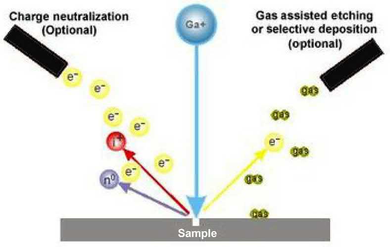
1.4.2Focusedionbeamlithography Focusedionbeamlithographyisanothernanomanufacturingtechniquesimilartoelectron beamlithography,buthereionsareusedtoperformthelithographyinsteadofanelectron beam( Fig.1.12 ).Sincetheionsaremuchheavierthanelectrons,focusedionbeam lithographycanbemoreefficientthanelect ronbeamlithography.Thefocusedionbeam lithographytechniquealsoh assomedifferentclassifica tions,butdirectwritingisthe simplestandcheapestoneandhencethatistheonediscussedhere.Inthismethod,aresistis notusedandbyvaryingthedistanceofthewafer,thedoseofionscanbecontrolled,resulting
Fig.1.11
(A)ConceptualdiagramofDiVa:1.Planarcathode,2.Shapingapparatus,3.Shapingapparatus secondset,4.deflector,5.Wafer,6.Deflectionplates;(B)ExperimentalDiVaapparatusatStanford University [47]
Fig.1.12
Schematicdiagramoffocusedionbeamlithography.
inatrenchofdifferentdepthonthewafer.Heavy-ionspeciessuchasGa+ andAu+ canalsobe usedinthislithographytoproduceastronger effect.Whenabeamispassedoverthewafer,a trenchhavinginverseGaussianshapeisobta ined.Withincreaseinstrength,thetrench becomesmoresharp,narrow,andV-shaped [48].Multiplepassesarealsopossibletocreate complicatedshapes.
1.4.3X-raylithography X-raylithography(XRL)isanadvancedversionofopticallithographyinwhichshorter wavelengthsareused.Inthismethod,aspecialtypeofmaskisusedwithdifferentlocalX-ray absorptionareastodefinethepattern.ThispatternisreplicatedonanX-raysensitivematerial calledaresist,whichispreviouslydepositedonasubstrate(usuallyasiliconwafer).Whenthe X-raypassingthroughthepatternfallsontheresist,itmaycausecross-linking(fornegative resists)orbondbreaking(forpositiveresists),dependingonthechemicalnatureoftheresist. Afterexposure,thewholethingisdippedinaspecificsolventand,dependingonitsnature, eithertheexposedarearesistwilldissolveandcreateapatternorviceversa.Theotherpartof theresistwillstayintact [49].ThisishowX-raylithographycreatesnanopatternsonthe substrate.
1.5Conclusionsandfuturedirections Thebeginningsofnanotechnologyarepopularlydatedbacktothefamouslecturegivenby NobellaureateRichardFeynman,“There’sPlentyofRoomattheBottom,”in1959.Butthe applicationofthistechnologybecameevidentatthebeginningof1980.Sincethen, nanotechnologyhasgainedhugemomentumandcurrentlyisbeingappliedinvariousaspectsof