Humanizing Healthcare Summer Knight
https://ebookmass.com/product/humanizing-healthcare-summer-knight/ ebookmass.com
SeriesEditors
C.P.Wong,ShengLiuandWenhuiZhu
Modeling,Analysis,Design, andTestsforElectronics
PackagingbeyondMoore
HengyunZhang
EasternScholarProfessor,SchoolofMechanicaland AutomotiveEngineeringShanghaiUniversityofEngineering Science,Songjiang,Shanghai,China
FaxingChe
ResearchScientist,InstituteofMicroelectronics, A*STAR,Singapore
TingyuLin
GeneralManagerAssistant,NationalCenterforAdvanced Packaging,Wuxi,China
WenshengZhao
Assoc.Professor,SchoolofElectronicsandInformation, HangzhouDianziUniversity,Hangzhou,Zhejiang,China
WoodheadPublishingisanimprintofElsevier
TheOfficers ’ MessBusinessCentre,RoystonRoad,Duxford,CB224QH,UnitedKingdom 50HampshireStreet,5thFloor,Cambridge,MA02139,UnitedStates TheBoulevard,LangfordLane,Kidlington,OX51GB,UnitedKingdom
Copyright©2020ChemicalIndustryPressCo.,Ltd.Allrightsreserved.Publishedby Elsevier,Inc.underanexclusivelicensewithChemicalIndustryPressCo.,Ltd.
Nopartofthispublicationmaybereproducedortransmittedinanyformorbyanymeans, electronicormechanical,includingphotocopying,recording,oranyinformationstorage andretrievalsystem,withoutpermissioninwritingfromthepublisher.Detailsonhowto seekpermission,furtherinformationaboutthePublisher’spermissionspoliciesandour arrangementswithorganizationssuchastheCopyrightClearanceCenterandthe CopyrightLicensingAgency,canbefoundatourwebsite: www.elsevier.com/permissions. Thisbookandtheindividualcontributionscontainedinitareprotectedundercopyrightby thePublisher(otherthanasmaybenotedherein).
Notices
Knowledgeandbestpracticeinthis fieldareconstantlychanging.Asnewresearchand experiencebroadenourunderstanding,changesinresearchmethods,professional practices,ormedicaltreatmentmaybecomenecessary.
Practitionersandresearchersmustalwaysrelyontheirownexperienceandknowledgein evaluatingandusinganyinformation,methods,compounds,orexperimentsdescribed herein.Inusingsuchinformationormethodstheyshouldbemindfuloftheirownsafety andthesafetyofothers,includingpartiesforwhomtheyhaveaprofessionalresponsibility.
Tothefullestextentofthelaw,neitherthePublishernortheauthors,contributors,or editors,assumeanyliabilityforanyinjuryand/ordamagetopersonsorpropertyasamatter ofproductsliability,negligenceorotherwise,orfromanyuseoroperationofanymethods, products,instructions,orideascontainedinthematerialherein.
LibraryofCongressCataloging-in-PublicationData
AcatalogrecordforthisbookisavailablefromtheLibraryofCongress
BritishLibraryCataloguing-in-PublicationData
AcataloguerecordforthisbookisavailablefromtheBritishLibrary
ISBN:978-0-08-102532-1
ForinformationonallWoodheadPublishingpublicationsvisitour websiteat https://www.elsevier.com/books-and-journals
Publisher: MatthewDeans
AcquisitionEditor: KaylaDosSantos
EditorialProjectManager: PeterAdamson
ProductionProjectManager: JoyChristelNeumarinHonestThangiah
CoverDesigner: ChristianJ.Bilbow
TypesetbyTNQTechnologies
Abouttheauthors

HengyunZhang isaprofessorinShanghaiUniversityofEngineeringScienceand EasternScholarProfessorconferredfromShanghaiEducationCommission.He obtainedBachelordegreeandMasterdegreefromUniversityofScienceand TechnologyofChinain1994and1997,respectively,andPhDdegreefromNanyang TechnologicalUniversityin2001.Aftergraduation,heworkedinindustriesand researchinstitutesfor18years,includingInstituteofMicroelectronics(Singapore), AdvancedMicroDevicesandDowCorning.Heworkedonnearly20projectsas projectandtechnicalleaders.HewastherecipientsofITHERMBestPosterPaper Awardin2004,AMDEngineeringExcellenceAwardin2008,andIceptBestPaper Awardin2010.Hehasmorethan80publicationsinInternationaljournalsand conferencesandmorethan30patentsgranted/ filedintheUnitedStates,Singapore, andChina.Healsoservedascommitteemembersforanumberofinternational conferences(IEEEITHERM,ICEPT,EPTC,ASMEMNHMT).Hehasbeen reviewersfornearlytwentyjournalpublications.Hewasoneofthefoundermembers inthethermalmanagementassociationofChinaelectronicscommittee.

FaxingChe isaresearchscientistwithInstituteofMicroelectronics(IME),Agency forScience,TechnologyandResearch,Singapore.HereceivedBEdegreein mechanicalengineeringandMEdegreeinsolidmechanicsfromUniversityofScience andTechnology,Beijing,China,in1995and1999,respectively,andPhDdegreein engineeringmechanicsfromNanyangTechnologicalUniversity,Singapore,in2006. Hehas13years’ experienceinthedesign-for-reliabilityforadvanced electronicspackaging.HeworkedwiththeUnitedTestandAssemblyCentre, STMicroelectronics,andInfineonTechnologiesSingapore.Hehasauthoredand coauthoredmorethan120technicalpapersinrefereedjournalsandconferences,and thecitationsgivenbyGoogleScholararecloseto2000.Dr.Cheservesasapeer reviewerformorethan10journals.HewastherecipientsofBestPosterPaperAward fromEPTC2013,BestPosterPaperAwardfromITHERM2006,BestPaperAward fromICEPT2006,andOutstandingStudentPaperAwardfromEPTC2003.
TingyuLin isGeneralManagerAssistantofNationalCentreforAdvancedPackaging (NCAP),China,andNational “ThousandPeoplePlan” Expert.Hehasmorethan 20years’ experiencesindesign,process,assembly,reliability,andequipment developmentinelectronicspackaging,semiconductor,consumerelectronics,and thermalandaerospaceindustry.HereceivedBEdegreeinthermalengineeringfrom TsingHuaUniversityandMEdegreeinaerospaceengineeringfromtheMinistryof
Aerospace,China,in1990andPhDinmicroelectronicsfromNationalUniversityof Singapore(NUS)in1997.HewasaMotorola(Google)-certifi edSixSigmaBlackBelt in2012.From2012 13,hewasaprogramdirectorofInstituteofMicroelectronics, Singapore(IME),andresponsiblefor2.5D,fan-outandWLPdevelopment.From 1997 2012,heworkedasaseniormanagerinPhilips,LucentTechnologies,the formerAT&TBellLab,andMotorolaElectronics,respectively.Untilnow,hehas beenengagedinmorethan100productdesignandprocessdevelopmentinmobile modules,ICcomponents,andconsumerelectronics,etc.Hehaspublished150papers and fi ledmorethan10patents,obtainedmanybestpaperawardsandgavekeynote talksinseveralconferences,andledtwointernationalASTMstandardsforTSV development.

Wen-ShengZhao isanassociateprofessorwithHangzhouDianziUniversity.He obtainedBachelordegreefromHarbinInstituteofTechnologyin2008andPhD degreefromZhejiangUniversityin2013.HewasavisitingPhDstudentatNational UniversityofSingaporefrom2010to2013andavisitingscholaratGeorgiaInstitute ofTechnologyfrom2017to2018.Hiscurrentresearchinterestsincludeinterconnects designandsimulation,carbonnanoelectronics,andmultiphysicssimulation.Hehas publishedover70papersininternationaljournalsandconferences(morethan20IEEE papers).Heservedasapeerreviewerformorethan10internationaljournals.Hewas thereceiptofBestStudentPaperAwardfromIEEEEDAPS2015.
Preface
Inmorethan50years,themiraculousdevelopmentofsemiconductordeviceshasbeen witnessedbytheincreasingnumberandshrinkinggatesizeoftransistorsinthe integratedcircuit(IC)chipandpackaging.From2transistorsinthe fi rst-generation ICbyJackKilbyin1959toaround5billiontransistorsinthelatestprocessorfora mobilephone,thescalingofMoore’slawhasbeenrelentlesslyfollowed.Because ofthephysicallimitations,thedevicescalingwouldstopatthe7 5nmtechnology node.Instead,moreandmoreattentionisbeingpaidontheheterogeneousandhybrid integrationofmultiplechipsinapackage.Dissimilarchipssuchascentralprocessing units,memory,graphicprocessingunits,RFchips,MEMSsensors,andopticaldevicesaretobeintegratedintoonepackage,whichisoftencalledasmorethanMoore (MtM)orbeyond-Mooretechnologies.Newapplicationssuchasmobilecommunication,cloudcomputing,bigdata,InternetofThings,energystorageandconversion, automaticdriving,and,morerecently,artificialintelligencearebecomingthedriving forcesfortheinnovationofelectronicdevicesandsystems.
Manyadvancedelectronicpackagingarebeingconceptualizedandmanufacturedto meetthevariousapplicationscenarios.Amongthem,the2.5Dand3DICpackaging andtheirhybridcombinationsareviewedasthemostpromisingtechnologies.Fan-out wafer-levelpackagingprovidesalow-costheterogeneousintegrationsolutionfor multiplechips.
Thecombinationofthesepackagingtechnologyleadstoincreaseddesign complexity,decreaseddesignmargins,andincreasedpossibilityoffailureinsignal integrity,process,thermalperformanceandreliability,whichmayhamperthetechnicalprogress.Manyeffortshavebeenmadeonthedevelopmentof2.5Dand3D packagesbasedonthrough-siliconvia(TSV)technologiestoaccumulateexperience andknowledgeinthenewareas.Withtheincreasingdevelopmentinpackagingarchitectureandconcepts,itisimportanttounderstandthenewphenomenaandmechanism associatedwiththepackages.Themodeling,simulation,andanalysistoolswithvalidatedaccuracyandefficiencyaretobedeveloped,thoughnotyet,atthesamepaceto addressthenewissuesandtopredictandguidethepackagingdesignandprocess.A properuseofthemodelingandanalysistoolcangreatlysavedesigntime,minimize thedefects,andshortenthetimetomarket.
Nonetheless,fundamentalunderstandingswitheffectiveanalysistoolsarestill lackinginthepredictionofelectricalandthermalperformanceandthermomechanical reliability.Newchallengesandissuesrelatetovariousaspects:thecrosstalkbetween TSVs,thethermalperformancewithinsulatedTSVs,thermalmanagementfor3DIC
packagingwithinterveningheating,thermomechanicalstressinBEOLlayersand TSVs,thecopperextrusioninTSVs,issuesinthecarbonnanotubeinterconnects, andsoon.Processdevelopersareoftenplaguedbythecontradictoryresultsduring theassemblyprocessortestatendofline.Duringtheassemblyof2.5Dpackage withchip-on-wafer-on-substratetechnology,chip-on-chip(CoC) fi rst,ortheCoC onsubstrate(CoC-oS)technology,warpageofpackagewithTSVinterposercanbe convexorconcave,whichisdif ficulttoexplain.Onlyafterrepeatedtrialswithoutsuccess,theprocessengineersstarttounderstandandtreattheissuesseriouslybyseeking helpfromtheexperiencedresearcherswithmodelingexperienceandskills.
Developmentofhighlyefficientanalysismodelandsubmodelswithprovedcases arecrucialtothesuccessfuldevelopmentofelectronicpackaging.Undoubtedly,there existschallengesinthemultiphysicsmodelingforelectronicpackagingwhichcouples electrical,thermal,andmechanical fi eldsintheassemblyprocesses,end-of-line,and reliabilitytests.The2.5D/3DICpackagemayhavegoodelectricalperformancebut isbottleneckedbythepoorthermalperformanceofinterstrabondinglayers.A comprehensiveunderstandingofthenewpackagesisimportanttotheresearchers frombothindustryanduniversities.
Thisbookisprimarilyconcernedwiththemodeling,analysis,design,andtestof electronicpackagingforheterogeneousintegrationintheerabeyondMoore’slaw. Itmainlyfocusesonthe2.5D/3DpackagingwithTSVsandwith fine-lineRDLinterconnects.Fundamentaltheoriesandnewadvancesinelectrical,thermal,andthermomechanicalorthermohygromechanical fieldsarecovered.Theelectricallyand thermallyinducedissuessuchaselectromagneticinterferenceandhotspotsarerelated topackagesignalandthermalintegrity,whereasthethermomechanicalstressisrelated tothepackagestructuralintegrity.Notonlythebasicprinciplesinelectrical,thermal, andmechanicalareaswillbepresentedbutalsothemodelingandanalysistechniques relatedtopracticaltechnologiessuchaswaferlevelpackagesand2.5D/3Dpackaging willbeanalyzed.Someofthenewmaterialmodelingandtestingmethodologiesare alsoincludedtoaddressthechallengesrelatedtothenewpackagedevelopment.
Thisbookisintendedfordesignengineers,processingengineers,andapplication engineersaswellasforpostgraduatestudentsmajoredinelectronicspackaging. Exempli fiedcasestudiesarealsodemonstratedtosatisfytheinterestsofengineers andresearchersspecializedinthisdomain.
Alltheauthorshavebeenengagedintheelectronicspackagingindustry,research institutes,anduniversitiesfortenyearsandabove,withsomeauthorsformorethan20 years.Theauthorshavebeenfullyinchargeofandsupportofanumberofpackage developmentprojectswithin-depthexperienceandknowledge.Morethan80%of thecontentisbasedontheauthors’ personalexperienceandprofessions.
TherehavebeenseveralbooksinEnglishareavailabletoreadersintheMtM electronicspackaging.However,mostofthemarelimitedtotheconceptualization ofarchitecture,electrical,andprocessevaluation,withoutdetailedmodelingandverifi cationinthethermalandelectricalperformancesandthermomechanicalstress.Their scopeisalsolimitedtoacertaindiscipline.Thisbookaddressesthe2.5D/3Dpackages fromthethreemajordisciplineswithvalidatedmodels,design,andtests,inhopeto
stimulatethedevelopmentofnewpackagingtechnologies,predictivemodels,testing methods,andevenanewsystem.
Thecontentofthisbookisarrangedinsevenchapters.
Chapter1introducesthebackgroundofthisbook.Itcoversthehistoricalevolution andbasicperformancemetricsofICpackaging,contributedbyalltheauthors.The challengesandsolutionsarealsocovered.Chapters2 5coverthedifferentaspects ofpackaging.InChapter2,thefundamentalofelectricaldesignandmodelingisintroduced,andthe3Dpackageandintegratedpassivesarebeingdiscussed,contributedby Dr.WenshengZhao.Chapter3addressesthebasicheattransfertheoriesandanalysis modelfromthermalviewpoints,contributedbyDr.HengyunZhang.Bothin-package andon-packagethermalsolutionsareanalyzed,tested,anddiscussed.Applicationsof newmaterialssuchascarbonnanotubeandgraphenearealsohighlighted.Dr.Faxing ChecontributetoChapter4,inwhichthestressandreliabilityanalysisofpackaging interconnectsarediscussed.Stress strainrelationship,nonlinearmaterialbehavior includingviscoplastics,creep,andviscoelasticmaterialmodels,andcharacteristic testsarecovered.Designforreliabilityusing finiteelementanalysisandsimulation hasbeendemonstratedforstacked-diepackageswithcasestudies.Chapter5presents ananalysisonthepackagefailuresrelatedtothermal,thermomechanical,andthermohygroswellingaspects,ascontributedbyDr.TingyuLin.BothDr.ZhangandDr.Che contributetothelasttwochapters,withChapter6coveringthepackageandmaterial thermalandmechanicaltesttechniquessuitableforelectronicpackagingandChapter7 thesystem-leveldesignandmodeling.
HengyunZhang,Ph.D. EasternScholarProfessor ShanghaiUniversityofEngineeringScience, Shanghai,China
FaxingChe,Ph.D. ResearchScientist InstituteofMicroelectronics, A*STAR,Singapore
TingyuLin,Ph.D. GeneralManagerAssistant NationalCenterforAdvancedPackaging, Wuxi,China
WenshengZhao,Ph.D. Assoc.Professor HangzhouDianziUniversity, Hangzhou,Zhejiang,China
Acknowledgments
Ithasbeenapainstakingyetfulfillingjourneytodocumentourpractitionerexperience turningintoanofficiallyprintedbook.Initiation,planning,andpreparationof Modeling,Analysis,DesignandTestforElectronicPackagingbeyondMoore were facilitatedbytheeditorsatChemicalIndustryPress,ElsevierPublisher,coauthors, andcolleaguesalloverus.Wewouldliketothankthemall,withspecialacknowledgmentstoMs.GangWuandMs.YufengLifromChemicalIndustryPress.Thisbook wouldhavenotbeencompletedwithouttheirprofessionaldedicationandinspiration. Thematerialsinthisbookhavebeenderivedfrommanypublishingorganizations, forwhichwehavepublishedsomematerialspreviouslyandreusedtheminthisbook. Weattempttoacknowledgehereforthehelpandsupport.TheyareInstituteof ElectricalandElectronicEngineers(IEEE),AmericanSocietyofMechanicalEngineers(ASME),andElsevierPublisherfortheconferenceproceedingsandjournal publicationsincludingIEEETransactionsonComponentsandPackagingTechnology, IEEETransactionsonDeviceandMaterialsReliability,ASMETransactionson JournalofElectronicPackaging,ASMETransactionsonJournalofHeatTransfer, AppliedThermalEngineering,MicroelectronicsReliability,JournalofAlloysand Compounds,InternationalJournalofRefrigeration,andJournalofElectronic Materials.ImportantconferencessuchasElectronicComponentsandTechnology Conference,IntersocietyConferenceonThermalandThermomechanicalPhenomena inElectronicSystems,ElectronicsPackagingTechnologyConference,andInternationalConferenceonElectronicPackagingTechnology & HighDensityPackaging arealsoappreciatedforauthorizingthereproductionofsomeofpublicationmaterials. Wewouldalsoliketoacknowledgethosewhohelpedreviewsomechaptersand sectionofthisbook.TheyareProfessorYalingHefromXi’anJiaotongUniversity, ProfessorJohanLiufromShanghaiUniversity,ProfessorXinweiWangfromIowa StateUniversity,Dr.XiaowuZhangfromInstituteofMicroelectronics,Singapore, ProfessorAndrewA.O.TayfromSingaporeUniversityofTechnologyandDesign, andProfessorJohnPangfromNanyangTechnologicalUniversity,Singapore.We wouldliketothankthemfortheirinsightfulsuggestionsandcommentsbenefiting tothisbook.Thehelpandsupportfromtheex-colleaguesincludingY.C.Mui,D.Pinjala,M.Rathin,W.H.Zhu,B.S.Xiong,L.H.Xu,D.Y.R.Chong,M.B.Yu,O.K. Navas,G.Y.Tang,B.L.Lau,L.Bu,DanielM.W.Rhee,andY.Hanareappreciated. Wealsothanktheanonymousreviewersfortheirconstructivereviewandcomments. The firstauthorwouldliketothankShanghaiUniversityofEngineeringSciencefor providingtheworkingenvironmenttomakethisbookpossible.The firstauthoralso
Acknowledgments
wouldliketoexpressthankstothepostgraduatestudentsfortheirwork,whichhelped preparethematerialsinthisbook.TheyareYangSui,LeJiang,ZehuaZhu,Xiaoyu Wu,andYuchenDeng.
Wewouldliketoacknowledgethesupportofthefundingagenciesinthepastyears suchasNationalNaturalScienceFoundationofChina(51876113,61874038),China 02NationalKeyProjects,InstituteofMicroelectronicsfromAgencyforScience, Technology,andResearch,Singapore,andNanyangTechnologicalUniversity, Singapore.
HengyunZhang,Ph.D. EasternScholarProfessor SchoolofMechanicalandAutomotiveEngineering ShanghaiUniversityofEngineeringScience Songjiang,Shanghai,China
FaxingChe,Ph.D. ResearchScientist InstituteofMicroelectronics,A*STAR Singapore
TingyuLin,Ph.D. GeneralManagerAssistant NationalCenterforAdvancedPackaging Wuxi,China
WenshengZhao,Ph.D. Assoc.Professor SchoolofElectronicsandInformation HangzhouDianziUniversity Hangzhou,Zhejiang,China
1.1Evolutionofintegratedcircuitpackaging
1.1.1Evolutionofintegratedcircuitdevicesandapplications
Integratedcircuit,shortenedasIC,byitsname,isthecombinationofmorethanone electricdevicesuchastransistorsandcapacitorsontoasemiconductorchipmadeof siliconorothermaterialstofulfillacertainfunctions.Electronicpackagingisreferred toastheelectricalandmechanicalconnectionsofICchiptoasystemboardtoforma standaloneelectronicproductorcanbeinterconnectedwithotherpackagestoforman electronicproduct.Asystemmayconsistofeitherstandaloneorinterconnected electronicproductswiththeneededfunctions.Theelectronicproductcanbeanalogizedwithahumanbody.WiththebrainasanICchip,theskullactsasmechanical protectionpartofthepackaging,andthebloodcirculationandnervoussystemact asthepower/groundconnectionsandsignaltransmissionlines.Thermalcoolingof thehumanbrainisimplementedthroughthenaturalconvectionfromtheheadas wellastheheatexchangethroughthedualfunctionofthebloodcirculationtothe body.Allthesensoryorgansworkassensorsonthepackagetocommunicatewith theouterworld.
ThedevelopmentofICdeviceshasbeenwitnessedbytheincreasingnumberand decreasinggatesizeoftransistorsintheICchipandpackaging.The firsttransistorwas inventedin1947,butthe firstICdevicewasdevelopedonlyafter12years.In1959, JackKilbyfromTexasInstrumentsintegratedtwotransistorsandaresistorinsilicon withalargespacingof7/16inch,whichwasconsideredasthebirthofmodernIC. Eversince,theIChasbeenevolvinginthescalingoftransistorgatesizeaspredicted byMoore’slaw.Today,ithascometoastagethattherearemorethan5billion transistorsinthelatestprocessorofamobilephoneandevenmoreforacomputer processor.In2016,AlphaGobecamethe firstcomputerGoprogramtobeatahuman professionalGoplayerwithouthandicapsonafull-sized19 19board.Behindthis sensationalhuman machinecompetitionwere50tensorprocessingunitsspeci fically developedformachinelearning.
Thedownscalingtothenanoscaleelectronicsbringsfundamentalandapplication issuessuchaselectricalcrosstalk,thermal,andmechanicalstressmanagement.Fundamentaltransportprocessesinthenanoscaledevicesareplayingaroledifferentfrom thatinthemacroscopicscale.Newdesigns,processes,andmaterialsarebeingpushed
2Modeling,Analysis,Design,andTestsforElectronicsPackagingbeyondMoore
tothelimitstomeetthechallengesinthepackagingfromthebackendoflineofwafer foundrytothepackagingandassemblyhouse.
Becauseofthephysicallimitations,thedevicescalingcouldstopatthe7 5nm technologynode.Ontheotherhand,moreandmoreattentionsarebeingpaidon theheterogeneousandhybridintegrationofmultiplechipsanddevicesinonepackage. Dissimilarchipssuchascentralprocessingunits,memory,graphicprocessingunits (GPUs),RFchips,microelectromechanicalsystemssensors,andopticaldevicesare tobeintegratedintoonepackagetoformahigherlevelofsystem-in-packageassembly withenhancedfunctionalityandimprovedoperationcharacteristics.Thisisoften calledasMorethanMoore(MtM)orbeyond-Mooretechnologies.
Variousapplicationssuchasmobilecommunication,cloudcomputing,bigdata, Internetofthings,energystorageandconversion,automaticdriving,and,more recently,artifi cialintelligencearebecomingthedrivingforcesfortheinnovationof electronicdevicesandsystems.Manyoftheapplicationsarehighlyrelatedtothe high-performanceelectronicpackagingandsystemswithheterogeneousintegration insteadoftheMoreMooreminiaturization.Suchtechnologycrossroadisillustrated in Figure1.1.1.Theverticalaxisin Figure1.1.1 indicatesthetrendofminiaturization withtheMoore’slaw,whereasthehorizontalaxisindicatesthetrendofMtMtechnology [1].Typicalapplicationsarelistedin Figure1.1.2[2]
More than moore: more function
devices Sensors activators Biochips
Interaction with people and environment nondigital content System in package (SiP)
High-valuesystem
Figure1.1.1 Semiconductortechnologyroadmapontheheterogeneousintegration.
1.1.2Evolutionofintegratedcircuitpackaging
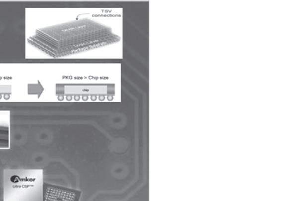
Thedevicescalingalsoaffectstheinterconnectsatthepackagingandsystemlevel.To connectthetransistorswithdownsizedscaletotheouterworld,moreintermediate layersarerequiredtofacilitatetheconnections,moreI/Osarerequiredtodistribute thepowerandsignallines,andmoreeffi cientyetcomplicatedcoolingtechnologies arerequiredtorejecttheexcessiveheatfromtheICandinterconnectsaswell.The evolutionoftheelectronicpackagesisillustratedin Figure1.1.3[2].
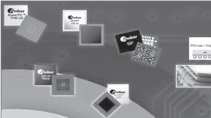
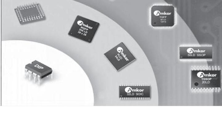
Asshownin Figure1.1.3,semiconductorpackagesareexperiencing fivemajor patternsduringlast fivedecades,whicharelead-frame,organicsubstratewithsolder balls(BGA),fan-inwafer-levelchip-scalepackage,fan-outwafer-levelpackaging (FOWLP),andthrough-siliconvia(TSV)technologyfor2.5D/3DICstacking, respectively.
DIP(dualin-linepackage)lead-framepackagesdominatedin1950 70,followed byQFP,PLCC,andSOICduring1980.TSSOPandTQFPweremuch finerpitched lead-framepackagesin1990.Atthesametime,BGApackageappearedandgradually
Figure1.1.2 Applicationstodrivetheelectronicproducts.
dominatedinthemarket.After2000,thereweremanypackagesshowingoffinthe formof flipchipBGA, flipchipCSP,etc.Wafer-levelpackages(WLPs)weremajor packageformatduetolowcost.StackedCSP,fan-inWLPs,andfan-outWLPsare graduallyburgeoninginthemarket.Especiallyfan-outWLPisbecomingamature technologyafter2010.
Inthetrendofshiftingfromtheconventionalplanar2Dchippackagingtothe3D packaging,advancedelectronicpackagingformatsaretobeconceptualized,designed, andmanufacturedtomeetthevariousapplicationscenarios.Amongthem,the2.5D and3DICpackagingandtheirhybridcombinationareviewedasthemostpromising technologies.FOWLPprovidesalow-costalternativeforheterogeneousintegration solutionaheadofthe3Dchipstacking.Theinitialpackage-on-packagecameafter 2000andgraduallydevelopedtoa3Dpackagestackindifferentformssuchaswire bondingandmixof flipchip.
Manyeffortshavebeenmadeonthedevelopmentof2.5Dand3Dpackagesbased onTSVtechnologieswithaccumulatedexperienceandknowledgeintheheterogeneousareas [3 5].Thegeneraltechnologytrendtowardthe3DICpackaginghas beenshownin Fig.1.1.3.Atypical3DICpackagereliesontheTSVtechnologyas theenablinginterconnects,drivenbythememorystack,wideI/O,logic þ memory, and field-programmablegatearray(FPGA)package.
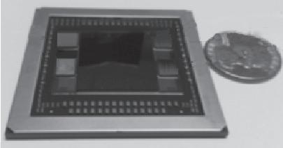
The fi rstcommercialproductin2.5Dpackageasshownin Figure1.1.4(a) was releasedbyXilinxin2010,withFPGAchipsonapassiveTSVinterposer(TSI)after severalyearsofinternaldevelopment.ManyothercompaniesalsoannouncedtheTSV technologyforproductexecution.Forexample,TSMCrevealed3DICdesignbased onsiliconinterposerinJune2010.Elpida,PTI,andUMCannouncedthestacksof logicandDRAMwith28nmtechnologyin2011,Microndevelopedthehyper memorycubein2011,andSamsungdemonstratedwideI/Omemoryformobile products.In2015,AMDannouncedtheirGPUcard,whichhasmorethan190,000 microbumpsandtheTSVinterposerhasmorethan25,000C4bumps.Thisisthe first GPUontheinterposeratasizeof1011mm2,withthemostdiesinasinglepackageas illustratedin Figure1.1.4(b),whichalsotookseveralgenerationsofimprovements beforeitsannouncement.The3D-stackedpackagesarealsobeingdeveloped,with muchfasterprocessingspeedandreducedtotalpowerdissipation,suchasforthe wide-bandwidthmemory.Thestackingoflogicdiestogetherisalsoofgreatinterest recently.Nonetheless,mostoftheworkislimitedtotheresearchlevelwithoutbeing commercializedduetothetechnicaldif ficultiesinareassuchasprocessabilityand thermalmanagement.
1.1.3Challengesandsolutions
Asithasbeendemonstrated,theheterogeneousintegrationofthedifferentchipsand technologiesinapackageleadstoincreaseddesigncomplexity,decreaseddesign margins,andincreasedpossibilityoffailureinsignalintegrity,process,thermal management,andreliability,whichmaygreatlyslowdownthetechnicalprogress anddesigntime.Withtheincreasingdemandforpackagingarchitectureandconcepts inmoreapplications,itisimportanttofosterthedesignmethodology,modelingand 4Modeling,Analysis,Design,andTestsforElectronicsPackagingbeyondMoore
Figure1.1.4 (a)Xilinx first2.5Dthrough-siliconvia(TSV)digital field-programmablegate array(FPGA)and(b)AMDRadeongraphiccardwithHBMsurroundingthegraphic processingunit(GPU)inasingle2.5Dpackage.
analysistools,manufacturing,andreliabilitytestcapacityassociatedwiththe2.5D/3D ICpackagedevelopment.
Thecorrespondingmodeling,simulation,andanalysismethodologiesdescribing theprocess,performance,andreliabilityareurgedtodevelop,thoughdifficult,at thesamepacetoaddressthenewissuesandtopredictandguidethedesignand process.Themodelingandanalysismethodologiesshouldbephysicallyrobustand validatedwithengineeringaccuracyandefficiency.Aproperuseofthemodeling andsimulationtoolcangreatlysavedesigntime,minimizethedefects,andshorten thetimetomarket.Emphasisshouldbeputontheelectricalandthermalmodeling ofinterconnectsandTSVs,themechanicalstress,thecoupledmultiphysicsinteractionsduringprocess,andthereliabilityor fi eldtests.Theeffectsofmicroscaleand nanoscaleonthedevices,dielectrics,andinterfacialmaterialsshouldalsobe considered.
1.2.1Electricalperformanceanddesignmethodology
Withtherapiddevelopmentanddownscalingofsemiconductortechnology,thenumber offailurescausedbythesignalintegrityproblemsintheintegratedsystemisontherise. SignalintegrityisreferredtoasabroadsetofICdesignissuesrelatedtointerconnects, suchasreflection,crosstalknoise,andelectromagneticinterference [6].Thegoalof signalintegrityanalysisistoensurehigh-speeddatatransmissiontoguaranteereliable systemoperation.Powerintegrityproblemisanothersetofproblemsalongthepower andgroundpaths.Theobjectiveofthepowerintegrityanalysisistoensurethedesired voltageorcurrentfromthesourcetothedestination.Obviously,worsesignalandpower integritywouldresultinperformancedegradationandevencausesystemstofail.
Theimpedance,whichisdefi nedastheratioofthevoltagetothecurrent,isthekey parameterintheelectricaldesign.Itiscommonlyusedinthesignalandpowerintegrityevaluation.Forexample,thewaytominimizethesignalreflectionduetothe impedancemismatchisessentialtokeeptheimpedanceatthesamelevelthroughout thenet.Withrespecttothepowerdistributionnetwork(PDN),theimpedanceisused asthecriterion.Tokeepthevoltageripplelowerthanthespeci fication,itisessentialto reducethePDNimpedancebelowthetargetimpedanceatallthefrequencies supportedbythesystem.
Ina3DICpackaging,multiplechipsarestackedverticallywiththesignaltransmittedthroughTSVs.AlthoughTSVsprovideshorterinterconnectlengthandthereby reducepowerconsumptionandarea,theyhavetobeelectricallyisolatedfromthebulk silicon.Thecapacitiveloadinginducedbythethininsulatorlayerandlossyeffect wouldcauseaconsiderabledegradationinthesignalquality.Moreover,thenoise couplingbetweenTSVsandaTSVandactivedevicesbecomesmorecriticalwith theincreasingTSVdensity,asshownin Figure1.2.1.Thepowerdeliveryin3DintegratedsystemisalsoamajorconcernasTSVsproduceadditionalinductanceeffects,
Figure1.2.1
leadingtohighpeaksofPDNimpedance.Withtheincreaseinstackeddies,itis predictedthatthepowerdensitypersquareareaofthe3DICincreasesbyafactor ofN0.5,whereNisthenumberofstackeddies,indicatingthatmorepowerdelivery isneededwiththeincreasingnumberofdies [7].
Toevaluatethesignalandpowerintegrity,circuitmodelingcanbecarriedoutto provideanin-depthphysicalunderstanding.Inthisbook,theequivalentcircuit modeloftheTSVsisdevelopedwiththec onsiderationoftheMOScapacitance effect.Theinfl uenceofthe fl oatingsiliconsubstrateontheTSVcapacitanceis alsoconsidered.Toguaranteesignalintegrity,theschemesofcoaxialstructure anddifferentialsignalinga reinvestigated.ThePDNimpedanceisalsostudiedbased ontheequivalentcircuitmodel,whichcouldprovidesomeusefulguidanceforthe designof3DICpackaging.
1.2.2Thermalperformanceanddesignmethodology
Duringelectronicoperation,heatisgeneratedinthechipandalongtheinterconnects duetoohmicheatingandpowerdissipationduetohigh-frequencyswitching.In contemporaryportableelectronicproducts,theelectrochemicalheatgenerationfrom thebulkybatteriesmaynotbeignoredandshouldbeconsideredinthesystemdesign. Theobjectiveofthermaldesignistoensurethatthetemperaturesofthecomponentsin asystemaremaintainedwithintheirfunctionaltemperaturerange.Withinthetemperaturerange,acomponentisexpectedtomeetitsspecifiedperformancewithoutexcessiveperformancedegradationandoreventhermalrunway [8],whichislikelyto damagethesystem.
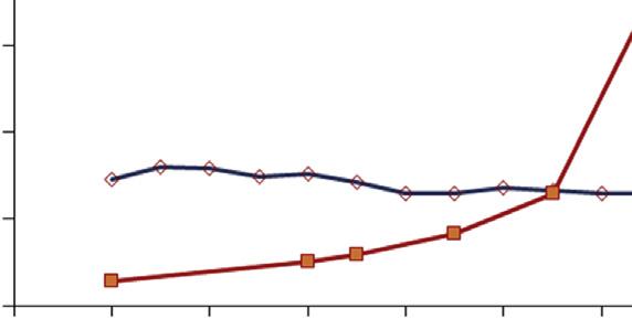
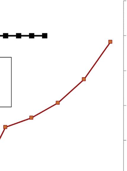
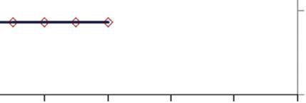
Inthedesignofelectronicpackaging,thethermaldesignpower(TDP)isusedasthe targetofthermaldesign.Thisisthemaximumpowerthatthechipandpackagecan dissipateduringoperation,whichdefinestheupperlimitofpowerdissipation.Given theTDP,thejunctiontemperatureshouldbemaintainedwithinacertaintemperature levelwithrespecttotheprescribedambientcondition.Inaprocessorchip,the projectedpowerdissipationisaround130W,levelingofffromthetransistorscaling asshownin Figure1.2.2.
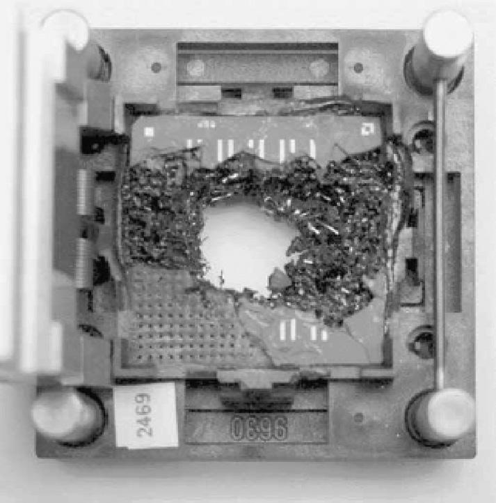
Intheabsenceofappropriatethermaldesign,logicerrorsoreventhermalrunaway wouldoccur,whichmaycausepermanentfailureinchipandpackage.Oneexampleof thedamagedpackageduetothermalrunaway [8] isindicatedin Figure1.2.3.The targetofthermaldesignistoensurethatthecomponentsoperatewithintheprescribed temperaturelimitbasedontheambientconditionatthegivenTDP.Inotherwords,the thermalresistanceshouldbekeptwithinthespeci fiedthermalresistance,whichis definedbythedifferenceofthejunctiontemperaturetoreferencetemperatureover powerdissipation.Thefollowingtwothermalresistancesarecommonlyusedinpackagethermalcharacterizationandarethereforeintroducedtodescribethethermal performance.Thejunctiontoambientthermalresistance Rja indicatestheheatdissipationcapacityfromthechiptothesurroundingenvironment,whereasthejunctionto casethermalresistance Rjc refl ectsthepackagethermalperformance.Thelowerthe thermalresistanceis,themoreeasilytheheatcanbedissipatedandthelongerlife thepackagecansurvive.
8Modeling,Analysis,Design,andTestsforElectronicsPackagingbeyondMoore
Cost performance chip High performance chip
Figure1.2.2 Thethermaldesignpower(W)forthesinglechipandthefacilitycoolingpower forthedatacenterracks.
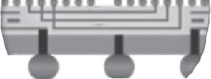
Thermalrunawayofapackageunderstressedtest.
Thethermaldesigncanbeimplementedthroughapproachessuchasthermally enhancedpackagematerials,structuralimprovement,andheatsinkdesignandoptimization.Thepositionofthermalpackagingengineeristhuscreatedtocoverthethermal design,modelingandanalysis,materialscharacterization,andqualifi cationalongwith theelectricalengineerandmaterialsandprocessengineer.
Withthedevicescalingandheterogeneousintegration,a2.5D/3Dpackage integratedwithmultiplechipsisbeingdevelopedasthenextgenerationofpackage. Ina2.5Dpackage,dissimilarchipscanbeassembledonacommoninterposertofulfill
Figure1.2.3
theoperationsthroughthemicrolinesandTSVinterconnects,whereasa3Dpackage requiresthemultiplechipsbeingverticallystacked,withTSVsandmicrobumpsas interconnects.TSVsserveasacommoninterconnecttechnologyina2.5Dand3D forshortenedsignaltransmission,lessdelay,andmorefunctionality.Theshiftto theheterogeneousintegrationleadstonewthermalmanagementissuessuchasthermal crosstalkandthermalblockingalongthethermalpath.
Properevaluationandcharacterizationofthethermaltransportpropertiesof3D chipsandtheinterconnectsarethe firststeptothesuccessfulthermaldesignofthe package.Ontheotherhand,thedeterminationofthermalperformanceiscomplicated withvariousdesignfactorsincludingvariouspackageelements,geometricalstructure, andmaterialtypes,whichmaynotbesolvedbyasingleanalysisapproach.
Inthisbook,differentlevelsofthermalanalysisanddesignmethodsaretobe addressed.Analyticaltechniquebasedonporousmediatheoryiswiselysoughtto resolvethethermalpackageissueswithvariousrepeatedorrandomstructuresand materialcompositions.Ontheotherhand,numericaltoolsarecommonlyutilizedto resolvethethermalpackageintegratedinthesystemwithdifferentlevelsofpackage elementsandboundaryconditions.Nonetheless,packagesubmodelsplayanimportant roleandshouldbedevelopedinthenumericalmodeltosimplifythemodelingefforts andtime.
Lastbutnottheleast,thethermaldesignandanalysisaretobecomparedandverifiedwiththeexperimentaltests,whichconstitutesasolidstepinutilizingthenumericalanalysisasoptimizationtoolforimplementingthepackagedesign.
1.2.3Stressandreliabilityissues
Electronicproductsusedbothinindustriesandbyconsumersareexpectedtofunction reliablyinserviceanduserenvironment.Electronicpackagingisatechnologyfor fabricatingandassemblingICchipsintoelectronicproducts.Electronicpackage providesnotonlyelectricalinterconnectionsbutalsothemechanicalsupportfor protectingtheelectroniccircuits [9].Itisimportanttoensuretheelectronicproducts withdesignedfunctionandperformanceduringthespeci ficperiodofuserenvironment,especiallyforsecurityandsafetydemandingapplicationssuchasaerospace, automobiles,medicalequipment,andmilitaryelectronicsequipment.Thereliability ofapackagedmicroelectronicsystemisrelatedtotheprobabilitythatwillbeoperationalwithinacceptablelimitsforagivenperiodoftime [10].
Reliabilityofsemiconductordevicesandproductsmaydependonassembly process, fi eldapplication,andenvironmentalconditions.Stressfactorsaffecting device/productreliabilityincludevoltage,currentdensity,temperature,humidity, mechanicalorthermomechanicalstress,vibration,shockandimpact,gas,dust,salt, contamination,radiation,pressure,andintensityofmagneticandelectrical fields [11].Whentheappliedstressishigherthanstrengthofmaterialitself,materialwill degradeatafasterpace,exhibitingductileorbrittlefailures.Evenwhentheapplied stressislessthanthestrengthofmaterial,thematerialmayexhibitfatiguefailure whensubjectedtocyclicloadssuchastemperaturecycling,powercycling,andcyclic bending.Inreality,materialstrengthisnotaconstantandmaydegradewithtimeunder
hightemperatureorhighhumiditycondition,whichusuallyresultsininterfacial delaminationorcrackingfailure.
Themethodologyofdesign-for-reliability(DFR)contributestohighqualityand reliableelectronicassemblies,includingthe2.5Dand3Dpackages.Electronicassembliesaretestedathigherstressconditionstoacceleratefailureforquickunderstanding ofproductreliability [12].Theacceleratedlifetestmethodsshortenthecycletimefor reliabilitydesign.Reliabilitytestssuchasthermalcycling(TC)andthermalshock (TS),cyclicbending,powercycling,high-temperaturestorage,vibrationtests,drop impact,highlyacceleratedtemperatureandhumiditystresstest,unbiasedautoclave, andcombinedtestingcanprovideusefulfailureassessmentmethodsforreliability ofelectronicassemblyandproduct.Insitumeasurementisessentialtodetermine failuretime,whichisusuallyachievedthroughdaisychainorotherstructuredesign tomeasureresistanceorcapacitance.Samplesizeshouldfollowtherequirementof theteststandards.Reliabilitydatacanbeanalyzedbyreliabilitystatisticaldistribution model,suchasnormaldistribution,exponentialdistribution,andthecommonlyused Weibulldistributionmodel.
Inreliabilitystudy,failureanalysis(FA)isimportantto findfailurelocationsand revealfailuremodesforunderstandingfailuremechanism.TheFAofmicroelectronic productsinvolvestheuseofvariousFAtoolsandtechniques.Scanningacoustic microscope(SAM)isonenondestructiveFAtoolindetectingcracks,voids,and delaminationswithinmicroelectronicpackagesandassemblies.Tolocalizethefailure location,thecross-sectioningtechniquecombinedwiththefocusedionbeametching isusedforsamplepreparation,andthenopticalmicroscopeorSAM,eventransmissionelectronmicroscope,isusedfortakingfailureimagestodeterminefailurelocation andfailuremodeaccompaniedwithahighlost.Dyepenetrationmethodisawidely appliedandlow-costmethodtolocatefatiguecracksinmicroelectronicassembly, suchassolderjointcrackingunderrepeatimpactdroptestorTCtest.
Inadditiontofailurelocationidentification,stressanalysisisessentialtobetter understandfailuremechanism.Finiteelementanalysis(FEA)providesapowerful toolinnumericalmodelingandsimulationofstressinelectronicspackages.FEA modelingandsimulationcanhelpreproducethefailureprocess,reducetheassessment time,andprovideacomprehensivefailureassessment.
Fortheadvancedpackages,thesolderjointisoftentheweakestlink,andsolder jointreliabilitybecomesevenmoreimportantwithfurtherminimizationofelectronic assemblies.ThesolderjointisparticularlypronetofatiguefailureduetopowerandTC loading [13].TCandvibrationtestsarecommonlyusedforcharacterizationofsolder jointfailureassessment.TCloads(high-strain,low-cyclefatigue)induceviscoplastic deformationinthesolderjoints.Vibrationloads(low-stress,high-cyclefatigue) primarilyinduceelasticorelastic plasticdeformationinthesolderjoints.Drop impacttestisusedtoinvestigateimpactreliabilityofelectronicassembliesforportable electronicproducts.
FEAsimulationprovidesimportantunderstandingonthemicrodeformation responsesinsolderjointsubjectedtoreliabilitytestconditions.Thecombinationof FEAsimulationandreliabilitytestsprovidesaneffectivetoolforDFRapplication inexistingandnewelectronicpackagingdesigns.Itshouldbekeptinmindthata 10Modeling,Analysis,Design,andTestsforElectronicsPackagingbeyondMoore
Materials
Solder
Substrates
Chip
Underfill
Metal pad
Mold compound
Others
Failure mode analysis
Bulk solder fatigue
Solder/IMC interface
fracture
IMC/Cu pad interface
fracture
Chip cracking
Lead cracking
Accelerated testing
Thermal cycling/shock
Cyclic bend
Drop impact
Vibration
Combined loading
Material properties
Young’s modulus
Poisson ratio
Yield stress Density
CTE
Temperature and/or strain rate dependent
Design for reliability
Life prediction Models
Stress-based
Strain-based Energy-based Facture mechanics Miner’s law
Constitutive models
Elastic Plastic
Viscoelastic
Viscoplastic
Creep
Elastic–plastic–creep
Isotropic/orthotropic
FE modeling
Geometry 2D versus 3D
Material properties
Loading
Boundary condition
Submodeling
Stress–strain curve
Energy output
Design optimization
Geometry
SMD versus NSMD
Underfill or not
Pb-based versus Pb-free
Surface finish
Figure1.2.4 Themultidisciplinaryapproachindesign-for-reliabilitymethodology.
multidisciplinaryapproachisrequiredforelectronicassemblyfailureassessments. Figure1.2.4 showsthedetailedanalysisanddesignmethodologyinDFRmicroelectronicassembly.
References
[1]Heterogeneousintegration,ITRS2.0, www.itrs.net
[2]TheDevelopmentTrendandChallengesofCommunicationProducts,CaiXi,Huawei technologiesCo.,LTD,2014.
[3]J.Lau,TSVinterposer:themostcost-effectiveintegratorfor3DICintegration,in:ASME Interpack,2011,p.52189.
[4]L.L.Yin,C.K.K.Keng,G.Tan,2.5D/3DdevicepackageleveldefectLocalizationwiththe useofmultiplecurvetracingsandrepeatedthermalemissionanalyses,in:Proc.EPTC, 2015,pp.287 290.
[5]C.-C.Lee,C.P.Hung,etal.,AnoverviewofthedevelopmentofaGPUwithintegrated HBMonsiliconinterposer,in:Proc.ECTC,2016,pp.1439 1444.
[6]E.Bogatin,SignalandPowerIntegrity Simplifed,PearsonEducation,2010.
[7]N.H.Khan,S.M.Alam,S.Hassoun,Powerdeliverydesignfor3-DICsusingdifferent through-siliconvia(TSV)technologies,IEEETrans.VeryLargeScaleIntegr.Syst.19(4) (2011)647 658.
[8]A.Vassighi,O.Semenov,M.Sachdev,CMOSICtechnologyscalinganditsimpacton burn-in,IEEETrans.DeviceMater.Reliab.4(2)(2004)208 220.
12Modeling,Analysis,Design,andTestsforElectronicsPackagingbeyondMoore
[9]M.Pecht,HandbookofElectronicPackageDesign,MarcelDekker,Inc.,NewYork,1991.
[10]R.R.Tummala,FundamentalsofMicrosystemsPackaging,McGraw-Hill,2001.
[11]G.DiGiacomo,ReliabilityofElectronicPackagesandSemiconductorDevices,McGrawHill,1996.
[12]H.A.Chan,P.J.Englert,AcceleratedStressTestingHandbook-GuideforAchieving QualityProducts,IEEEPress,2001.
[13]J.H.Lau,ThermalStressandStraininMicroelectronicsPackaging,VanNostrand Reinhold,NewYork,1993.
Furtherreading
[1]W.Chen,HIRRoadmapWorkshopPresentation,2017. http://cpmt.ieee.org/technology/ heterogeneous-integration-roadmap.html