Dedication
Dedicatedtoallthepeopleforthebettermentoftheirlife
1.Thefundamentalaspectsofspintronics1
1.1Introduction1
1.2Fundamentalaspectsofspintronics4
1.3Deviceprinciples12
1.4Differentspintronicsapplications,deviceprinciples,and devices14
1.5Conclusion17 References19 Furtherreading21
2.Introduction:carbonandcarbonnanomaterials23
2.1Introduction23
2.2Carbonandcarbonnanostructurematerialsinspintronics23
2.3Differentformsofcarbonandcarbonnanostructurematerials25
2.4Conclusionandperspectivesofcarbonandcarbon nanostructure-basedspintronicsapplications36 References37 Furtherreading45
3.Magnetismandspintronicsinamorphous/diamond-like carbon47
3.1Introduction47
3.2Magnetismofamorphouscarbonanddiamond-likecarbon48
3.3Electricalandtransportofamorphouscarbonanddiamond-like carbon52
3.4Magnetoresistanceandspintronicsofamorphouscarbon anddiamond-likecarbon56
3.5Spinfieldeffecttransistor(FET)63
3.6Diamond-likecarbonformagneticstoragedisks67
3.7Conclusionandperspectivesofamorphouscarbonand diamond-likecarboninspintronics68 References69 Furtherreading73
4.Magnetismandspintronicsincarbonnanotubes75 4.1Introduction75
4.2Magnetismofcarbonnanotubes77
4.3Spintronicdevices83
4.4Spincurrentsinmagnetictunneljunctions87
4.5Tunnelmagnetoresistanceincarbonnanotube based spintronicdevices93
4.6Conclusionandperspectivesofcarbonnanotubesin spintronics97 References97 Furtherreading102
5.Magnetismandspintronicsingraphene103
5.1Introduction103
5.2Makingofgrapheneintomagneticmaterials105
5.3Spingenerationandspinmanipulation107
5.4Magnetismingraphene109
5.5SpinHalleffectandedge-derivedspinphenomena113
5.6Spininjection,manipulation,anddetection115
5.7Spinrelaxationprocess117
5.8Spinrelaxationinsingle-layergrapheneandbilayer graphene121
5.9Electricalspintransport123
5.10Spintronicsmagnetoresistancedevices129
5.11Applicationsofgraphenespintronics131
5.12Graphene-ferroelectricmeta-devices138
5.13Conclusionandperspectivesofgraphene-basedspintronics140 References142
Furtherreading150
6.Magnetismandspintronicsingrapheneoxide151
6.1Introduction151
6.2Magnetizationofgrapheneoxide153
6.3In-planeandout-of-planemagnetization/magnetic anisotropy165
6.4Magnetoresistanceofgrapheneoxide165
6.5Applicationsofgrapheneoxidespintronics172
6.6Conclusionandperspectivesofgrapheneoxide based spintronics176 References176 Furtherreading181
7.Magnetismandspintronicsincarbon nanoparticle/fullerene183
7.1Introduction183
7.2Carbonnanoparticle basedspintronics184
7.3Carbonnanospherespintronics186
7.4Graphene-nano-dotsspintronics188
7.5Fullerene-basedspintronics191
7.6Conclusionandperspectivesofcarbonnanoparticles based spintronics195 References196
8.Magnetismandspintronicsinothercarbon-based compositematerials201
8.1Introduction201
8.2Carbonnanostructure-metal/nonmetal/metal-oxide compositesinspintronics202
8.3Conclusionandperspectivesofcarbon-metal/nonmetal/ composite-basedspintronics210
References210
9.Challengesandemergingdirectionofcarbonnanostructure materialsinmagnetismandspintronics213
References214 Index217
Abouttheauthor
SekharChandraRay(PhD,UniversityoftheNorthBengal,India)isaB-ratedresearcherin PhysicsfromtheNationalResearchFoundation.Heiscurrentlyaprofessorofphysicsatthe UniversityofSouthAfricainexperimentalcondensedmatterphysics.Prof.Rayhailsfrom Indiawherehecompletedhisdoctoralstudieswhichfocusedmainlyonphotovoltaicsolar gradematerials.HehasworkedasaresearchfellowandvisitingscientistinItaly(INFM Fellow),Taiwan(NSCFellow),Spain(ICMM,CSIC,ForeignResearcherFellow,Ministryof ScienceandTechnology,Spain),SouthKorea(BrainPoolResearchFellow,Govt.South Korea),andIndia(IACS,VisitingScientist).Hisresearchgroupfocusesoncarbonnanostructurematerialinelectronicstructure/magneticpropertiesforthepossiblefabricationofspintronicdevicesapplicationandbioimagingprocess.Atpresent,Prof.Rayisworkingon different2D-structurematerialssuchas graphene, MoS2, stanene, silicene,and germanene. Duringhis22-yearresearchcareer,hehaspublished125peer-reviewedresearcharticles, includingsevenin NaturePublishingGroup (NPG)journalwithmorethan3800citationsin internationallyrecognizedjournals.Prof.Rayalsoactsasaneditorialboardmemberof ScientificReports NPGjournal.
Preface
Thisbookhasbeenwrittentomeetthebasicrequirementofresearchersgettingtrainingin carbonandcarbonnanomaterialsformagnetismandspintronicapplications.
Carbon-basedspintronicsrefersmainlytothespininjectionandtransportincarbon materialsincludingcarbonnanotubes,graphene,fullerene,andorganicmaterials.Inthelast decade,extraordinarydevelopmenthasbeenachievedforcarbon-basedspintronics,andthe spintransporthasbeenstudiedinbothlocalandnonlocalspinvalvedevices.Aseriesoftheoreticalandexperimentalstudieshasbeendonetorevealthespinrelaxationmechanisms andspintransportpropertiesincarbonmaterials,mostlyforgrapheneandcarbonnanotubes.Inthisbook,weprovideabriefreviewonspininjectionandtransportingraphene, carbonnanotubes,fullerene,andorganicthinfilms.
Thecontentsofthebookarefromdifferentarticlespublishedindifferentjournalsfrom differentresearchgroupsworldwide.I,theauthorofthisbook,amverymuchthankfulto thosepublishersandtheauthorsfromwhosepublicationswehavecollectedallusefulinformationthatarepresentedinthisbook.Thisbookconsistsofninechaptersnamely,fundamentalaspectsofspintronics,carbonandcarbonnanomaterials,magnetismandspintronics inamorphous/diamond-likecarbon,magnetismandspintronicsincarbonnanotubes,magnetismandspintronicsingraphene,magnetismandspintronicsingrapheneoxide,magnetismandspintronicsincarbonnanoparticles/fullerene,magnetismandspintronicsinother carbon-basedcompositesmaterials,andchallengesandemergencedirectionofcarbon nanostructurematerialsinmagnetismandspintronics.
Wehopethatthisbookwillbeusefulforallresearcherswhoareworkingonthis researchfield.
Anysuggestionstowarditsfurtherimprovementwillbethankfullyacknowledgedand incorporatedinthenexteditions.
Thefundamentalaspectsof spintronics
1.1Introduction
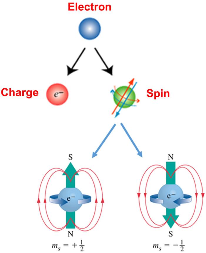
Informationtechnologyisoneoftheimportantissuesinthe21stcentury.AstheMoorelaw graduallylosesitseffect,conventionalcharge-basedelectronicswillcometoanendinthe nearfuture.Developingalternativehigh-speedandlow-energy-consuminginformationtechnologyisurgentlyneeded.Manynewmethodologieshavebeenproposed,suchasmolecular electronics,nano-electronics,spintronics,andquantuminformationtechniques,among whichspintronicsisoneofthemostpromisingones.Spintronicsisafieldofresearch exploitingtheinfluenceoftheelectronspinonelectricalconduction.Itismainlyknownfor the “giantmagnetoresistance” (GMR)(Baibichetal.,1998;Binashetal.,1989)andthelarge increaseoftheharddiskcapacityobtainedwiththereadheadsbasedonGMR.Butthe researchonspintronicshasalsorevealedmanyotherinterestingeffectsandisnowdevelopingalongpromisingnoveldirections.Comparedtoothermethodologies,spintronicsis compatiblewithconventionalelectronics,thusmanytechniquesusedinconventionalelectronicscanbedirectlyextendedtospintronics. “Spintronics, ” knownasspinelectronics, involvesthestudyofactivecontrolandmanipulationoftheintrinsicspinoftheelectrical chargeofelectronanditsassociatedmagneticmomentinsolid-statesystem.Theapproach inthefieldofelectronicsisbasedontheup-ordownspinofthecarriersratherthanonelectronsorholesasintraditionalsemiconductorelectronics.Itisdifferentfromconventional electronics,whichusestheelectron’schargedegreeoffreedomforinformationprocessing; spintronicsisdevotedtoincorporatingtheelectron’sspindegreeoffreedom.Inanidealsituation,therewillpurelybespincurrentandnochargecurrentinthespintronicscircuit, thusnoheatwillbecreatedandwasted.Therehasbeenagreatdealofrecentinterestinthe conceptof “spintronics” (Prinz,1995, 1998).Spintronicsisamultidisciplinaryfieldwhose centralthemeistheactivemanipulationofspindegreeoffreedominsolid-statesystem. Controllingandprobingspin-polarizedchargecarrier(ormanipulationofelectronspin)in semiconductorsand/ormetalsviaelectricalmeans,anattractiveroutetowardthedevelopmentofpracticalsemiconductor/metalspintronicdevices,whichareexpectedtohavea strongimpactonfutureinformationprocessingandstoragetechnologies.Itistheuseofa fundamentalpropertyofparticlesknownasspinforinformationprocessing.Itcarriesinformationinboththechargeandspinofanelectron,potentiallyoffersdeviceswithagreat diversityoffunctionalityinsolid-statedevicesandotherdevicesthatexploitspinproperties. Inthecaseoftheelectron,thespincaninfactassumeonlythevalues 1 1/2or 1/2:an eloquentinvitationtouseittoencodeinformation,inanalogytobits “0” and “1” ofthe
MagnetismandSpintronicsinCarbonandCarbonNanostructuredMaterials.DOI: https://doi.org/10.1016/B978-0-12-817680-1.00001-9 © 2020ElsevierInc.Allrightsreserved.
FIGURE1–1 Manipulationofelectronmovement(electronspin):spin-up(anticlockwise)andspin-down(clockwise). 2MagnetismandSpintronicsinCarbonandCarbonNanostructuredMaterials
binarycode(Fig.1 1).Inferromagneticmaterials,thespinoftheelectronscanbemodified fromtheoutside,applyingamagneticfield.Whenthemagneticfieldisremoved,thenew spinvaluesareretained,thatis,theencodedinformationremainsfirmlystoredwithout needforpowerandwithouttheriskofdemagnetization.
Spintransportandspinrelaxationinsemiconductorsandmetalsareimportantsolid-state physicsissuesthatareincludedinthefundamentalresearchalongwithnewtechnologybeing implementedintheelectronicstoragetechnology.Spintronicshelpedincreatingaprototype devicethatisusedintheindustryasareadhead,andamemory-storagecellisthe giantmagnetoresistive (GMR)sandwichstructure,whichconsistsofalternatingferromagneticand nonmagneticmetallayers.Dependingontherelativeorientationofthemagnetizationsinthe magneticlayers,thedeviceresistancechangesfromsmall(parallelmagnetizations)tolarge (antiparallelmagnetizations).Thischangeinresistance(alsocalledmagnetoresistance)isused tosensechangesinmagneticfields.Electronspincanbeidentifiedasamagneticfieldhaving oneortwopositions,knownas “ up ” and “down”.Thisgivesanextratwobinarystatestothe conventionalhighandlow-logicvalues,which arerepresentedbysimplecurrents.Whenthe spinstateisaddedtothemix,abitcanhavefourpossiblestates,whichcanbecalled “up-high” , “up-low” , “down-high,” and “down-low.” Thesefourstatesrepresentquantumbitsorqubits.
• Lowpowerconsumption
• Lesselectriccurrentrequired
• Fasterdevices
• Largerstoragecapacity
• Smallerdevices
• Lessheatdissipation
• Spintronicmemoryisnonvolatile
• Spinmanipulationisfaster,hencegreaterreadingandwritingspeed
Metallicspintronics hasalreadydeliveredfunctionaldevices(GMRreadheadsinlargecapacityharddiskdrives),andmagneticrandomaccessmemory(RAM)(MRAM),of insulatorspintronics [magnetictunneljunctions(MTJs)].Thebasicspinvalvehasevolvedtoa relatedthin-layeredstructure MTJ thatdisplaysgianttunnelingmagnetoresistance(TMR), aphenomenonwhereelectronstunnelthroughathininsulator.ThismeanstheTMRsignal ismuchlargerthanthatfromaGMRspinvalve:indeed,itisalmost100timeslarger.TMRis alsothebasisofmagneticRAM(MRAM),anonvolatilememorythatusesmagneticmoments toretaindatainsteadofelectricalcharges.
However,thecurrentbasicphysicsresearchismostlyfocusedon semiconductorspintronics.Althoughcreationofinhomogeneousspindistributiondoesnotrequireenergypenalty (incontrasttochargedistributionsofconventionalelectronics),spinisnotconservedwhereas chargeis.Thuseffortsinsemiconductorspintronicsresearcharefocusedonbasicproblems, suchascoherentmanipulationofelectronspinatagivenlocation,transportingspins betweendifferentlocationswithinconventionalsemiconductorenvironment,all-electrical spincontrolviaspin orbitinteractions,dilutedmagneticsemiconductors,andfixedor mobilespinqubitsforquantumcomputing.Otherpossibleapplicationsofspintronicsinclude high-speedmagneticfilters,sensors,quantumtransistors,andspinqubitsforquantumcomputers(Steane,1998;Lossetal.,1998;Burkardetal.,1999).Moreover,these “spintronic” devicesmightleadtoquantumcomputerandquantumcommunicationbasedonelectronic solid-statedevices,thuschangingtheperspectiveofinformationtechnologyinthe21st century.Morefundamentalresearchwill,however,beneededbeforeapracticalspintronic devicecanbedemonstrated,asmuchremainstobeunderstoodaboutspincoherence,spin entanglement,spindynamics,spinrelaxation,spintransports,etc. thedifferentfundamental aspectsofspintronics.
Spintronicsfacesanumberofchallenges,includingspingenerationandinjection,long distancespintransport,andmanipulationanddetectionofspinorientation.Insolvingthese issues,newconceptsandspintronicsmaterialswereproposedoneafteranother,suchas halfmetals,spin-gaplesssemiconductors,andbipolarmagneticsemiconductors.Topological insulatorscanalsobeviewedasaspecialclassofspintronicsmaterials,withtheirsurface statesusedforpurespingenerationandtransportation.Indesigningthesespintronicsmaterials,first-principlescalculationsplayaveryimportantrole.Inthissection,weattemptto giveabriefdiscussiononthebasicprinciplesandtheoreticaldesignofthesematerials. Meanwhile,wealsogivesomeattentiontoantiferromagnetic(AFM)spintronics,whichis mainlybasedonantiferromagnetsandhasarousedmuchinterestinrecentyears.
1.2Fundamentalaspectsofspintronics
Thefundamentalaspectsofspintronicsareunderlyingthegenerationofcarrier-spinpolarization,spincoherence,spinentanglement,controlspinandchargedynamics,spininjection, andspin-polarizedtransportinsemiconducting/metallicelectronicmaterials.
1.2.1Spinpolarization
Spinpolarizationisthedegreetowhichthespin,thatis,theintrinsicangularmomentumof elementaryparticles,isalignedwithagivendirection.Thispropertymaypertaintothespin, hencetothemagneticmoment,ofconductionelectronsinferromagneticmaterialsgivingrise tospin-polarizedcurrents.Spinpolarization,notonlyofelectrons,butalsoofholes,nuclei,and theexcitations,canbedefinedas PX 5 XS/X;wheretheratioofthedifference XS 5 Xλ X λ andthesum X 5 Xλ 1 X λ ofthespin-resolved λ componentsforaparticularquantity X.To avoidambiguityastowhatpreciselyismeantbyspinpolarization,boththechoicesofthe spin-resolvedcomponentsandtherelevantphysicalquantity X needtobespecified.
Conventionally, λ istakentobe m or 1 (numericalvalue 1 1)forspin-up,and k or (numericalvalue 1)forspin-down,withrespecttothechosenaxisofquantization(alongthespin angularmomentum,appliedmagneticfield,magnetization,ordirectionoflightpropagation). Inferromagneticmetals(FMs),itiscustomarytoreferto m (k)ascarrierswithmagnetic momentparallel(antiparallel)tothemagnetizationor,equivalently,ascarrierswith majority or minorityspin (Tedrowetal.,1973).Insemiconductorsthetermsmajorityandminorityusually refertorelativepopulationsofthecarrierswhile m or 1 and k or correspondtothequantum numbers mj withrespecttothe z axistakenalongthedirectionofthelightpropagationoralong theappliedmagneticfield(MeierandZakharchenya,1984; Jonkeretal.,2003).
1.2.2Spinrelaxation
Havingestablishedthatonecangeneratespin-polarizedearners,themostimportantissueis todeterminehowlongtheseelectronsremembertheirspinorientation.Thisisespecially importantforelectronicapplications,becauseifthespinsrelaxtoorapidly,thedistancestraversedbythespin-polarizedcurrentinadevicewillbetooshorttoserveanypracticalpurpose(Prinz,1995).Thespin spinrelaxationisthemechanismbywhich Mxy ,thetransverse componentofthemagnetizationvector,exponentiallydecaystowarditsequilibriumvaluein nuclearmagneticresonance(NMR)andmagneticresonanceimaging.Itischaracterizedby thespin spinrelaxationtime,knownas T2,atimeconstantcharacterizingthesignaldecay. Itisnamedincontrastto T1,thespin latticerelaxationtime.Itisthetimeittakesforthe magneticresonancesignaltoirreversiblydecay(37%i.e.,1/e)itsinitialvalueafteritsgenerationbytippingthelongitudinalmagnetizationtowardthemagnetictransverseplaneaccordingtothefollowingrelation: Mxy t ðÞ 5 Mxy 0 ðÞe t =T2 . T2 relaxationgenerallyproceedsmore rapidlythan T1 recoveryanddifferentmaterialshavedifferent T2.Whenexcitednuclear spins,lyingpartiallyinthetransverseplane,interactwitheachotherbythelocalmagnetic fieldin-homogeneitiesonthemicro-andnanoscales,theirrespectiveaccumulatedphases
deviatefromexpectedvalues.Whiletheslow-ornonvaryingcomponentofthisdeviationis reversible,somenetsignalwillinevitablybelostduetoshort-livedinteractions,suchascollisionsanddiffusion,throughheterogeneousspace. T2 decaydoesnotoccurduetothetilting ofthemagnetizationvectorawayfromthetransverseplane.
Spinrelaxationisverysensitivetotheelectronicbandstructure.Spinsofconduction electronsdecaybecauseofthespin orbitinteractionandmomentumscattering.Atlow temperatures(T # 20K),spinrelaxationiscausedbyimpurityscatteringandistemperature independent.Athighertemperatures,electronslosespincoherencebycollidingwith phonons(phononscaninduceaspinflipbecauseinthepresenceofaspin orbitcoupling, electronicBlochstatesarenotspinEigenstates).Spinrelaxationrate1/T1 increasesas temperatureincreases,withthegrowthbecominglinearabovetheDebyetemperature.This mechanism(Elliott,1954;Yafet,1963)isthemostimportantspinrelaxationmechanismin metalsandsemiconductorswithinversionsymmetry.
Differentspinrelaxationprocesseshavebeenfoundtobeimportantinsolids:
• Elliot Yafet
• D’yakonov Perel’
• Bir Aronov Pikus
• Hyperfineinteraction
Nonequilibriumdistributionofspinscausedbyinterfacesorspininjectionsisbrought backintoequilibriumbythesemechanisms,whichcanbeobstaclesforspintronics.Usually, suppressionsoftheseeffectsareimportantissuesinresearchanddevelopmentthough, sometimes,therelaxationwouldhelpfastdeviceaction.
1.2.3Spininjection
Spininjectioninanonmagneticmaterialis,inmostcases,achievedbythecreationofanonequilibriumspinpopulation(calledspinaccumulation)attheinterfacewithamagneticelectrode.Therateofspininjectiondependsonthespinrelaxationanddephasingmechanisms inthenonmagneticmaterial,whichtendstorestoretheequilibriumintheaccumulatedspin population;therelativelylonglifetimesofnonequilibriumelectronicspinsinsemiconductors andmetals,ofabout1ns,areessentialforspintronicdevices.Thespinlifetimescanhowever increasetohundredsofnanosecondsinconfinedsemiconductorheterostructures,which implytransportofcoherentspinpacketsoverhundredsof µm.
1.2.4Ohmicinjection
InanFMtheelectricalconductivityofthemajority-spin(spin-up)electronsdifferssubstantiallyfromminorityspin(spin-down),resultinginaspin-polarizedelectriccurrent.Themost straightforwardapproachtospininjectionistheformationofanohmiccontactbetweenan FMandasemiconductor,anticipatingaspin-polarizedcurrentinthesemiconductor. However,typicalmetal semiconductorohmiccontactsresultfromheavilydopingthe semiconductorsurface,leadingtospin flipscatteringandlossofthespinpolarization.
Followinguponearlierstudies(Johnsonetal.,1987;VanSonetal.,1987;Valetetal.,1993; HershÞeldetal.,1997)ofdiffusivespintransport,arecentworkby Schmidtetal.(2000) haspointedoutafundamentalproblemregardingohmicspininjectionacrossideal FM nonferromagnet(NFM)interfaces.Theeffectivenessofthespininjectiondependson theratioofthe(spin-dependent)conductivitiesoftheFMandNFMelectrodes, σ F and σ N, respectively.When σ F # σ N,asinthecaseofatypicalmetal,thenefficientandsubstantial spininjectioncanoccur,butwhentheNFMelectrodeisasemiconductor, σ Fcσ N,andthe spin-injectionefficiencywillbeverylow.Onlyforaferromagnetwheretheconductionelectronsarenearly100%spinpolarizedcanefficientspininjectionbeexpectedinthediffusive transport.Alargenumberofmaterialsapparentlyhavesuchhalf-metal-ferromagneticproperties(DeGrotetal.,1983;Kamperetal.,1988).Johnsonetal.haveproposedandpursued (Johnson1998,2001;Hammaretal.,1999,2000a,b)anapproachthatmayovercomethis obstacletospininjectionbytakingadvantageofthesplittingofthespindegeneracyofelectronsconfinedinasemiconductortwo-dimensional(2D)quantumwellstructure.Thesplittingisduetothespin orbiteffectthatcanarisefromanasymmetryintheconfining potential(Bychkovetal.,1994).Theresultcanbeaninducementofanonequilibriumspin polarizationifthe2Delectrongasiscarryingacurrent(Vorob’evetal.,1979).However,as intheohmiccontactexperiments,thesmallpercentagechangeindeviceresistance,thatis observedwithchangesinferromagnetorientation,hasledtosuggestionsofanalternative, local-Hall-effectexplanationforthedataandtootherquestionsregardingthisapproach (Monzonetal.,2000;Wees,2000;Hammaretal.,2000a,b).
1.2.5Tunnelinjection
AlvaradoandRenaud(Alvaradoetal.,1992),usingascanningtunnelingmicroscope(STM) withaferromagnetictip,showedthatavacuumtunnelingprocesscaneffectivelyinject spinsintoasemiconductor.Arecentextensionofthishasexaminedtheeffectofsurface structureonspin-dependentSTMtunneling( LaBellaetal.,2001).Thedevelopmentof FM-insulator FM-tunneljunctionswithhighmagnetoresistancehasalsodemonstrated thattunnelbarrierscanresultintheconservationofthespinpolarizationduringtunneling, suggestingthattunnelingmaybeamuchmoreeffectivemeansforachievingspininjection thandiffusivetransport.Theoreticalworkby Rashba(2000) hasquantitativelydeveloped theunderstandingofthepotentialeffectivenessoftunnelinjection.Iftheimpedanceofa barrierataninterfaceissufficientlyhigh,thenthetransportacrossthatinterfacewillbe determinedbythe(spin-dependent)densityoftheelectronicstatesofthetwoelectrodes thatareinvolvedinthetunnelingprocess.Thecurrentpassingthroughthebarrieristhen sufficientlysmallenoughfortheelectrodestoremaininequilibriumandtherelative (spin-dependent)conductivitiesoftheelectrodesplaynosubstantialroleindefiningor limitingthespin-dependenttransportacrosstheinterface.Thuseitherametal insulator semiconductortunneldiodeorametal semiconductorSchottkybarrierdiodethatusesan FMelectrodecanbeexpectedtobeaneffectivemeansforinjectingspinsintoasemiconductorsystem. 6MagnetismandSpintronicsinCarbonandCarbonNanostructuredMaterials
1.2.6Ballisticelectroninjection
Analternativetotunnelinjectionisspininjectionacrossferromagnet semiconductor interfacesintheballisticregime,withthe differencebetweenthetwospinconduction subbandsoftheFMandtheconductionbandofthesemiconductordeterminingthe spin-dependentinterfacialballisticelectr ontransmissionprobability.Itisgenerally assumedthatthetransversemomentumof anincidentelectronisconserved,and thisdeterminestheballistictransmissionan dreflectionprobabilitiesoftheinterface ( Kirczenow,2001;Grundler,2001 ).Also,onceaspin-polarize delectronentersthesemiconductorelectrode,theprobabilitythatitwil lbeelasticallyscatteredbackintotheferromagneticinjectormustbeverysmall.Ifthed evicedesignalsoinvolves,forexample,the spin-dependentcaptureofaninjectedcarrierbyanotherferromagneticelectrode,then transportthroughthesemiconductorregionmustbefullyballistic.However,iftheobjectiveissimplyefficientspininjection,athree-dimensionalballisticpointcontactbetween aferromagnetandasemiconductorshouldb eeffective.Recentexperimentswithpoint contactsformedbetweenferromagneticandnon-FMshavedemonstratedtheballistic point-contactinjectionofhigh( . 40%)spin-polarizedcurrentsintotheNFM( Upadhyay etal.,1998 , 1999 ).
1.2.7Hotelectroninjection
Anotherspintechniqueinvolvestheuseofpolarized “ hot ” electronsinjection,having energiesthataremuchgreaterthan E F ,bytunnel-injectingelectronsintoaferromagnetic layeratenergies cE F ( Monsmaetal.,1995;Jansenetal.,2001;Rippardetal.,2000 ). Asthemajority-spinandminority-spinelec tronshavemuchdifferentinelasticmeanfree paths,hotelectronpassagethrough,forexamp le,a3-nmColayer,issufficienttoresultin aballisticelectroncurrentth atismorethan90%polarized( Rippardetal.,2000 ).This highlypolarizedhotelectroncurrent canthencontinueontoanunderlying metal semiconductorinterfacewhereaportionofthebeamwillenterthesemiconductor,withthetransmissionprobabilitybei ngdeterminedbyenergyandmomentumconstraintsimposedbythebandstructuredifferencebetweenthesemiconductorandmetal attheinterface.Ifthereisnosubstantialspin flipscatteringattheinterface,theballistic electroncurrententeringthesemicond uctorwillalsobeveryhighlypolarized( . 90%), andtheinjectionenergy,re lativetothebottomofthesemic onductorconductionband, willbetunablethroughthetunnelinjectionbi as.Thedisadvantageofhotelectroninjectionisthattheoverallefficiencyislow.
1.2.8Spintransport
Particularinteresttothespintransporttheoryinsemiconductorsystemshasbeenthequestionastowhetherthequasiindependentelectronmodelcanadequatelyaccountforthe experimentalresults,orwhethermany-bodyorcorrelatedelectronprocessesareimportant. Thepresenceofspin-polarizedcarriersgivesrisetobothmodifiedchargetransportand
8MagnetismandSpintronicsinCarbonandCarbonNanostructuredMaterials
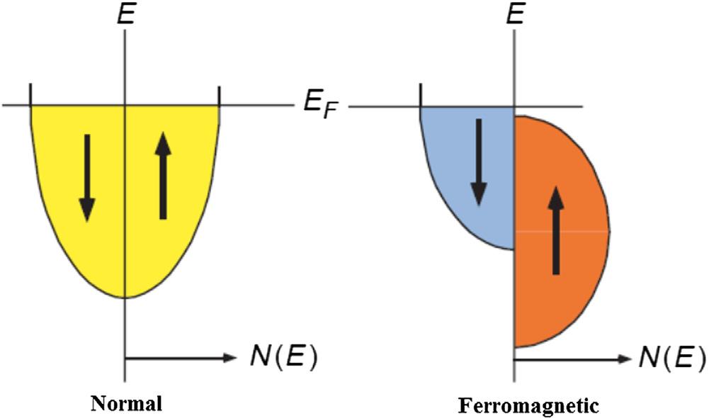
FIGURE1–2 Aschematicrepresentationofthedensityofelectronicstatesthatareavailabletoelectronsina normalmetalandinaferromagneticmetalwhosemajority-spinstatesarecompletelyfilled. E,Theelectron energy; EF,theFermilevel; N(E),densityofstates. CourtesyfromPrinz,G.A.,1998.Magneto-electronics.Science 282,1660 1663.
intrinsicspintransport,absentintheunpolarizedcase.Eachoftheseaspectsprovidesinformationaboutthedegreeofspinpolarization,whichcanbeutilizedinspintronics.Spinpolarizedtransportwilloccurnaturallyinanymaterialforwhichthereisanimbalanceof thespinpopulationsattheFermilevel.ThisimbalancecommonlyoccursinFMsbecause thedensityofstatesavailabletospin-upandspin-downelectronsisoftennearlyidentical, butthestatesareshiftedinenergywithrespecttoeachother(Fig.1 2).Thisshiftresultsin anunequalfillingofthebands,whichisthesourceofthenetmagneticmomentforthe materials,butitcanalsocausethespin-upandspin-downcarriersattheFermileveltobe unequalinnumber,character,andmobility.Thisinequalitycanproduceanetspinpolarizationinatransportmeasurement,butthesignandmagnitudeofthatpolarizationdepends onthespecificmeasurementbeingmade.Forexample,anFMmaybeusedasasourceof spin-polarizedcarriersinjectedintoasemiconductor,asuperconductor,oranormalmetal orcanbeusedtotunnelthroughaninsulatingbarrier.Thenatureofthespecificspinpolarizedcarriersandtheelectronicenergystatesassociatedwitheachmaterialmustbe identifiedineachcase.Themostdramaticeffectsaregenerallyseenforthemosthighly polarizedcurrents;thereforetherearecontinuingeffortstofind100%spin-polarizedconductingmaterials.ThesearematerialsthathaveonlyoneoccupiedspinbandattheFermi level.MaterialsthatareonlypartiallypolarizedsuchasFe,Co,Ni,andtheiralloys,which haveapolarization P of40% 50%(Soulenetal.,1998),are,however,adequatetodevelop technologicallyusefuldevices.Herethepolarization P isdefinedintermsofthenumberof carriers n thathavespin-up(nm)orspin-down(nk),as P 5 (nm nk)/(nm 1 nk).
Becauseofthespinpolarizationofanelectroncurrent,theeffectsseeninsolid-state devicescanbemostreadilyvisualizedifoneassumesthatthecurrentis100%polarized (Fig.1 2).Inthatcasetheonlystatesthatareavailabletothecarriersarethoseforwhich thespinsofthecarriersareparalleltothespindirectionofthosestatesattheFermilevel.If themagnetizationofthematerialsisreversed,thespindirectionofthosestatesalsoreverses.
Thusdependingonthedirectionofmagnetizationofamaterialrelativetothespinpolarizationofthecurrent,amaterialcanfunctionaseitheraconductororaninsulatorforelectrons ofaspecificspinpolarization.Ananalogycanbemadewithpolarizedlightpassingthrough ananalyzer.However,intheopticalcase,crossingthepolarizationaxisat90degrees preventsthetransmissionofthelight,whereasforspin-polarizedelectrons,themagnetizationmustberotated180degreestostopelectricalconduction.
Flatté(2001) hasextensivelyexaminedthisissueinthediffusivetransportregimeandhas concludedthatanindependentelectronapproachisquitecapableofexplainingmeasurementsofspinlifetimes,particularlytheroom-temperaturemeasurements. Shametal.(2000) and Sham(1999) havebeenfocusingontheverylowtemperatureregimewherecollective electronprocessesmaywellbeimportantindeterminingthespinrelaxationratesandspin lifetimes,althoughexperimentalresultsinthisregimearequitelimited.Onthedevicefront, Flatté(2001) hasconsideredthepossibilityofconstructingunipolarelectronicdevicesby usingferromagneticsemiconductormaterialswithvariablemagnetizationdirections.They haveshownthatsuchdevicesshouldbehaveverysimilarlytop ndiodesandbipolar transistorsandsuggestthattheycouldbeapplicableformagneticsensing,memory,andlogic.
1.2.9Spininjectionandspintransport
Spin-dependentelectrontransport,inbulkandnanostructures,isthepresenceofspinpolarizedcarriersthatgiverisetobothmodifiedchargetransportandintrinsicspintransport andareabsentintheunpolarizedcase.Eachoftheseaspectsprovidesinformationabout thedegreeofspinpolarizationthatcanbeutilizedinspintronics.Thetransportofspinpolarizedcarriersacrossthesemiconductor/metalinterfacewherethemetalisinthesuperconductingstate.Thestudyofsemiconductor/superconductorhybridstructureshasseveral importantramifications.Inthecontextofspinunpolarizedtransport(Lambertetal.,1998; Beenakker,1997),ithasbeendemonstrated(DeFranceschietal.,1998)thatthisconfigurationcanbeusedtoexaminetheinterfacialtransparencythatforasemiconductor/normal metalistypicallylimitedbyanativeSchottkybarrier.Inthepresenceofspin-polarized carriers,semiconductor/superconductorstructurecanalsoservetoquantifythedegreeof spinpolarizationofasemiconductorandprobebothpotentialandspin flipinterfacialscattering( ˇ Zuti ´ cetal.,1999).Tounderstandsuchsensitivitytospinpolarizationanddifferent typesofinterfacialscattering,itisimportanttoconsidertheprocessofAndreevreflection (Andreev,1964),whichgovernsthelowbiastransport.Inthistwo-particleprocess,anincidentelectronofspin σ 5 m,k onasemiconductor/superconductorinterfaceisreflectedasa holebelongingtotheoppositespinsubband,backtothesemiconductorregionwhilea Cooper(1956) pairistransferredtothesuperconductor.TheprobabilityforAndreevreflectionatlowbiasvoltageisthusrelatedtothesquareofthenormalstatetransmissioncoefficientandcanhavestrongerdependenceonthejunctiontransparencythantheordinary single-particletunneling.Forspin-polarizedcarrierswithdifferentpopulationsintwospin subbands,onlyafractionoftheincidentelectronsfromamajoritysubbandwillhavea minoritysubbandpartnerinordertobeAndreev-reflected.Inthesuperconductingstate,for
10MagnetismandSpintronicsinCarbonandCarbonNanostructuredMaterials
anappliedvoltagesmallerthanthesuperconductinggap,single-particletunnelingisnot allowedinthesuperconductorregionandthemodificationoftheAndreevreflection amplitudebyspinpolarizationorjunctiontransparencyismanifestedintransport measurements.
1.2.10Spindetection
Themostobviousapproachtotheelectricaldetectionofspinpopulationsinsemiconductors istousethespin-dependenttransportpropertiesofsemiconductor ferromagnetinterfaces. Experimentalefforts,withthisspin valvedetectionscheme,haveusedohmiccontactsfor thespin-collectionelectrode,butthesamedifficultiesdiscussedearlierapplytospincollection,anditappearsthatforeffectivespincollection/detection,eitheraballisticcontactora tunnelingcontactfromthesemiconductortoaferromagnetwillberequired.If,however,for reasonsofsignal-to-noise,anefficientspin-dependentextractionoftheinjectedspinpolarizedcurrentisrequired,thetunnelbarrierhastobesufficientlythinsothat (spin-dependent)tunnelingtransportintotheferromagneticelectrodeismoreprobablethan spinrelaxationwithinthesemiconductor(Rashba,2000).Analternativespindetectiontechniqueisapotentiometricmeasurement,withaferromagneticelectrode,ofthechemical potentialofthenonequilibriumspinpopulations(Hammaretal.,2000a,b;Johnson,2001). Withrespecttothecompletespintransistordevice,anextensiveanalysisby Tangetal. (2000) hasconcludedthatonlyforthecaseofballistictransportthroughoutthedevicestructurewillthedesired,electricalfield tunablespinprecessionbedetectableaspolarized electrontransitthroughthesemiconductorregion.Moreover,theyconclude,inaccordwith theinitialsuggestionof Dattaetal.(1990),thataverynarrow,single-orfew-electronchanneldevicestructurewillberequired.
1.2.11Spintransfer
Thespin-polarizedcurrentthatflowsfromonerelativelythick,andhencefixed,ferromagneticlayer,throughanonmagneticlayer,toanotherthin-film “free” nanomagnetcanby spin-dependentscatteringofthepolarizedcurrent(Berger,1996;Slonczewski,1996,1999) excitestrong,uniformspin-waveprocessionalmodesinthenanomagnet(Tsoietal.,1998; Myersetal.,1999;Rezendeetal.,2000).Intheabsenceofastrongexternalmagneticfield, thisspin-dependentscatteringcanalsoresultinthereversaloftheorientationofthemagneticmomentofthefreenanomagnetwiththefinalorientationrelativetothefixedlayer beingdependentonthedirectionofthecurrentflow(Katineetal.,2000).This “spin-transfer” processopensupthepossibilityofnewnanoscaledevicesformemoryandotherspinelectronicsapplications(Weberetal.,2001).Oneapplication,inadditiontodirectcurrent addressablemagneticmemory,mightbetheuseofspintransfertoexciteauniformspin waveinananomagnetandthentousethisnanomagnetasaprecessingspinfiltertoinjecta coherentspinpulseintoasemiconductorstructure.
1.2.12Spincoherence
Opticalpulsesareusedtocreateasuperpositionofthebasisspinstatesdefinedbyan appliedmagneticfieldandtheyfollowthephase,amplitude,andlocationoftheresulting electronicspinprecession(coherence)insemiconductors,heterostructures,andquantum dots.Thedataidentifiesnarrowrangesofdopingconcentrationswherespinlifetimesin semiconductorsareenhancedbyordersofmagnitude,culminatingintheobservationof spinlifetimesinsemiconductorsthatexceed100ns.Inheterostructuresandquantumdots, nanoseconddynamicspersisttoroomtemperature,providingpathwaystowardpractical coherentquantummagneto-electronics.
1.2.13Spinaccumulation
Whenspin-polarizedcurrentisdrivenfromaferromagneticfilmintoanonmagneticfilm, fasterthanthespinpolarization,itcandiffuseawayfromtheinterface,andanonequilibrium populationofspin-polarizedelectronsbuildsupinaregionofthicknessLs.Thisnonequilibriummagnetizationisdescribedasinequivalentchemicalpotentialsfortheupspinand downspinsubbandsofthenormalmetal.Thechemicalpotentialoftheferromagnet,however,isheldinequilibriumbytheintrinsicferromagnetic nonmagneticmetalinterface;this isthesameasaninternalelectricfield,associatedwiththenonequilibriumspinaccumulationthattriestodriveelectronsbackacrosstheinterfaceandintotheferromagnet.Because spinandchargearebothcarriedbytheelectron,agradientofspindensityresultsinan electricfield,whichcangeneratecurrentfloworproducedifferencesinvoltage(Johnson etal.,1987).Ifthemagneticmomentsofthetwoferromagneticlayersareparallel,spinaccumulationinthebasewillcreateanelectricfieldthatpushescurrentintothecollector,generatingapositivecurrentinthedetectorarmofthecircuit.If,however,themagneticmoments areantiparallel,thespin-accumulationelectricfieldatthebase collectorinterfacehasthe oppositesign,currentispulledfromthecollectorintothebase,andanegativecurrentis generatedinthedetectorarm.Thecurrentflowthroughthedetectorcanthusundergo bipolarmodulationbymodulatingthedirectionofmagnetizationinthesecondlayer.The devicemaybethoughtofasanonvolatilecomputermemoryelement,storinginformation viatheorientationofthesecondlayer.
1.2.14Coherentspintransportthroughsemiconductorsandinterfaces
Understandingthefundamentalpropertiesofspintransportinthesolidstateisessentialfor thedevelopmentofsemiconductor-basedspintronics.Inanalogytoconventionaldevices, whoseperformanceischaracterizedbycarriermobilitiesandlifetimes,spinmobilitiesand coherencetimesarefiguresofmeritforspintronicdevices.Recenttheoreticalworkhas shownthatitisessentialtoconsidertheinfluenceofelectricfieldsinducedbycarriermotion tounderstandthemotionofspinandthattheroom-temperaturespincoherencetimesin bulkandquantumwellstructuresappeartobedominatedbyprecessionaldecoherencedue tospin orbitcoupling(Flattéetal.,2000).Thesemodelsdescribehowthelow-fieldmobility
anddiffusionofspinpacketsdependsensitivelyonthedopingandrevealnewopportunities tocontrolspininteractionsbyengineeringstrainandcrystalorientation(Ohnoetal.,1999). Thespatialselectivityandtemporalresolutionofopticaltechniqueshavebeenusedtomonitorthedecoherenceanddephasingofelectronspinpolarizationduringtransportnotonly throughbulksemiconductorsbutalsoacrossheterojunctionsinengineeredstructures (Malajovichetal.,2000).
1.2.15Opticalcontrolofnuclearspins
Nuclearspinshavebeenproposedascandidatesforstoringbothclassicalandquantum informationbecauseofspinlifetimesthatexceedthoseofelectronsbyatleastseveralorders ofmagnitudeandthedegreeofcontrolprovidedbyconventionalNMRtechniques.The experimentalevidenceshowsthattheferromagneticmaterialscanbeusedtoimprint nuclearspinsinsemiconductors(Kawakamietal.,2001),therebyofferinganadditional pathwayformanipulatingandstoringinformationattheatomicscale.
1.2.16Quantumdots theartificialatomsinthesolidstate
Ithasbeenproposedthatthespinofanelectronconfinedtoquantumdotsisapromising candidateforquantumbitsandthatarrayofquantumdotscanbeusedinprincipletoimplementalarge-scalequantumcomputer(Lossetal.,1998;Burkardetal.,2000).Quantum operationsintheseproposalsareprovidedbythecouplingofelectronspinsinneighboring quantumdotsbyanexchangeinteractionbetweenthem.Thisinteractioncanbeswitchedby applyingcontrolledgatevoltagepulses,thusallowingrealizationoffundamentalquantum gatessuchastheexclusiveOR.Thereadoutofsuchaspinqubitcanbeperformedefficiently asaspin-polarizedelectriccurrentpassingthroughthedot(Engeletal.,2001)oroptically throughintegrationinsolid-statemicrocavities(Imamogluetal.,1999).Alternatively,qubit rotationscanbeimplementedbylocalelectrostaticshiftingoftheelectronintoaregionwith adifferenteffectivemagneticfield,suchasthatwhichoccursathetero-interfacesandin magneticsemiconductorstructures.
1.3Deviceprinciples
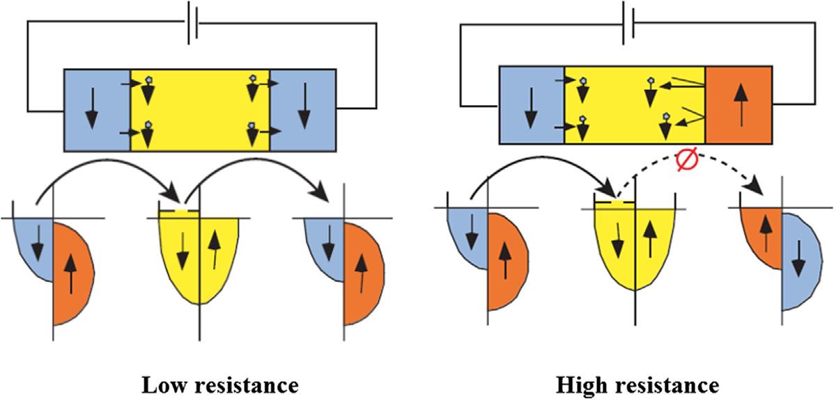
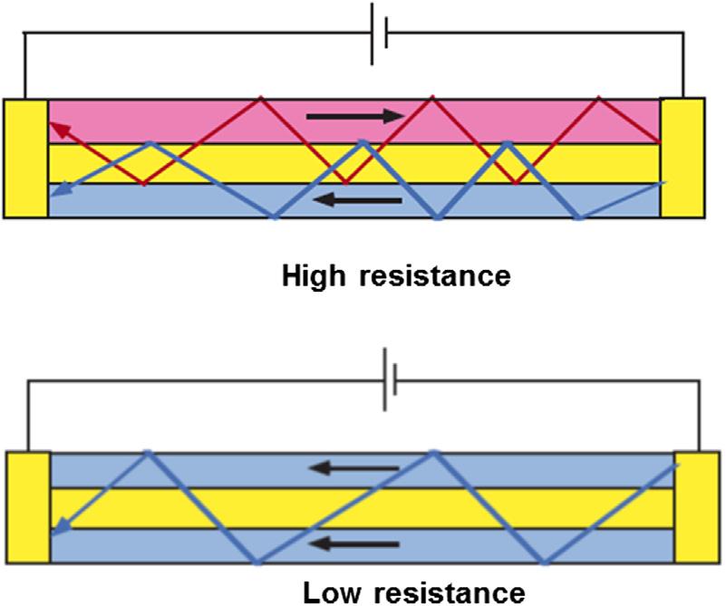
Thebasicactioninaspin-polarizeddeviceisshownin Fig.1 3,whereitisassumedthat theelectronsaretravelingfromanFM,throughanormalmetal,andintoasecondFM. Whenthemagnetizations(or,equivalently,themagneticmoments)ofthetwoFMsareinan alignedstate,theresistanceislow,whereastheresistanceishighintheantialignedstate. Actualdevicesarenotgenerallyfabricatedintheorientationshownin Fig.1 3,because theyaremadefromthinfilmsandtheresistanceperpendiculartotheplaneistoolow.The commonorientation,shownin Fig.1 4,providesmoreusefulresistance,butthephysical pictureofthespin-polarizedtransportismorecomplicated.Theeffectofthespinexclusion inantialignedfilmsisstillobserved,butitresultsinhigh-interfacescatteringand
FIGURE1–3 Schematicrepresentationsofspin-polarizedtransportfromaferromagneticmetal,throughanormal metal,andintoasecondferromagneticmetalforalignedandantialignedmagneticmoments. [,Disallowed channel. CourtesyfromPrinz,G.A.,1998.Magneto-electronics.Science282,1660 1663.
FIGURE1–4 Schematicrepresentationsoftransportthatisparalleltotheplaneofalayeredmagnetic-metal sandwichstructureforaligned(lowresistance)andantialigned(highresistance)orientations. Courtesyfrom Prinz,G.A.,1998.Magneto-electronics.Science282,1660 1663.
“channeling” ofthecurrentintonarrowedpathways(Fig.1 4).Whenthefilmsbecome aligned,bothoftheseresistance-generatingmechanismsareremoved,andthedeviceresistancedecreases.
Thissimpletwo-layersystemiscommonlyreferredtoasa “spinvalve” andisconstructed sothatthemagneticmomentofoneoftheferromagneticlayersisverydifficulttoreversein anappliedmagneticfield,whereasthemomentoftheotherlayerisveryeasytoreverse. Thiseasilyreversed(or “soft”)layerthenactsasthevalvecontrolandissensitivetomanipulationbyanexternalfield.Thedevicecanbeusedtomeasureormonitorthosefieldsand canhavenumerousapplications.