https://ebookmass.com/product/handbook-of-silicon-based-
Instant digital products (PDF, ePub, MOBI) ready for you
Download now and discover formats that fit your needs...
Modelling and Mechanics of Carbon-Based Nanostructured Materials. A volume in Micro and Nano Technologies 1st Edition Edition Duangkamon Baowan
https://ebookmass.com/product/modelling-and-mechanics-of-carbon-basednanostructured-materials-a-volume-in-micro-and-nano-technologies-1stedition-edition-duangkamon-baowan/ ebookmass.com
Literatures of Urban Possibility Markku Salmela
https://ebookmass.com/product/literatures-of-urban-possibility-markkusalmela/
ebookmass.com
3D and Circuit Integration of MEMS 1st Edition Masayoshi Esashi
https://ebookmass.com/product/3d-and-circuit-integration-of-mems-1stedition-masayoshi-esashi/
ebookmass.com
Living for Pleasure: An Epicurean Guide to Life Emily A. Austin
https://ebookmass.com/product/living-for-pleasure-an-epicurean-guideto-life-emily-a-austin/
ebookmass.com
Negotiating Peace: A Guide to the Practice, Politics, and Law of International Mediation (Ebook PDF)
https://ebookmass.com/product/negotiating-peace-a-guide-to-thepractice-politics-and-law-of-international-mediation-ebook-pdf/
ebookmass.com
The Law and Special Education (2-downloads)
https://ebookmass.com/product/the-law-and-specialeducation-2-downloads/
ebookmass.com
Wings of Starless Night (Kingsdaughter Book 1) Sadie Sterling
https://ebookmass.com/product/wings-of-starless-night-kingsdaughterbook-1-sadie-sterling/
ebookmass.com
Stop People Pleasing: How to Start Saying No, Set Healthy Boundaries, and Express Yourself Chase Hill
https://ebookmass.com/product/stop-people-pleasing-how-to-startsaying-no-set-healthy-boundaries-and-express-yourself-chase-hill-2/
ebookmass.com
Neuroscience
For Dummies, 3rd 3rd
Edition
Frank Amthor
https://ebookmass.com/product/neuroscience-for-dummies-3rd-3rdedition-frank-amthor/
ebookmass.com
https://ebookmass.com/product/the-sermons-of-john-donne-volume-10/
ebookmass.com
HandbookofSiliconBasedMEMSMaterials andTechnologies
HandbookofSiliconBased MEMSMaterials andTechnologies
ThirdEdition
Editedby
MarkkuTilli
OkmeticOy,Vantaa,Finland
MerviPaulasto-Kro¨ckel
SchoolofElectricalEngineering,AaltoUniversity,Espoo,Finland
MatthiasPetzold
FraunhoferInstituteforMicrostructureofMaterialsandSystemsIMWS,Halle,Germany
HorstTheuss
InfineonTechnologiesAG,Regensburg,Germany
TeruakiMotooka
KyushuUniversity,Fukuoka,Japan
VeikkoLindroos
SchoolofChemicalEngineering,AaltoUniversity,Espoo,Finland
Elsevier
Radarweg29,POBox211,1000AEAmsterdam,Netherlands
TheBoulevard,LangfordLane,Kidlington,OxfordOX51GB,UnitedKingdom 50HampshireStreet,5thFloor,Cambridge,MA02139,UnitedStates
Copyright©2020ElsevierInc.Allrightsreserved.
Nopartofthispublicationmaybereproducedortransmittedinanyformorbyanymeans,electronicormechanical,including photocopying,recording,oranyinformationstorageandretrievalsystem,withoutpermissioninwritingfromthepublisher.Detailson howtoseekpermission,furtherinformationaboutthePublisher’spermissionspoliciesandourarrangementswithorganizationssuch astheCopyrightClearanceCenterandtheCopyrightLicensingAgency,canbefoundatourwebsite: www.elsevier.com/permissions
ThisbookandtheindividualcontributionscontainedinitareprotectedundercopyrightbythePublisher(otherthanasmaybenoted herein).
Notices
Knowledgeandbestpracticeinthisfieldareconstantlychanging.Asnewresearchandexperiencebroadenourunderstanding, changesinresearchmethods,professionalpractices,ormedicaltreatmentmaybecomenecessary.
Practitionersandresearchersmustalwaysrelyontheirownexperienceandknowledgeinevaluatingandusinganyinformation, methods,compounds,orexperimentsdescribedherein.Inusingsuchinformationormethodstheyshouldbemindfuloftheirown safetyandthesafetyofothers,includingpartiesforwhomtheyhaveaprofessionalresponsibility.
Tothefullestextentofthelaw,neitherthePublishernortheauthors,contributors,oreditors,assumeanyliabilityforanyinjuryand/or damagetopersonsorpropertyasamatterofproductsliability,negligenceorotherwise,orfromanyuseoroperationofanymethods, products,instructions,orideascontainedinthematerialherein.
BritishLibraryCataloguing-in-PublicationData
AcataloguerecordforthisbookisavailablefromtheBritishLibrary
LibraryofCongressCataloging-in-PublicationData
AcatalogrecordforthisbookisavailablefromtheLibraryofCongress ISBN:978-0-12-817786-0
ForInformationonallElsevierpublications visitourwebsiteat https://www.elsevier.com/books-and-journals
Publisher: MatthewDeans
AcquisitionsEditor: SimonHolt
EditorialProjectManager: EmilyThomson
ProductionProjectManager: AnithaSivaraj
CoverDesigner: ChristianBilbow
TypesetbyMPSLimited,Chennai,India
1 Propertiesofsilicon3
MarkkuTilliandAtteHaapalinna
1.1Propertiesofsilicon3 References16
2. Czochralskigrowth ofsiliconcrystals19
OlliAnttila
2.1TheCzochralskicrystal-growing furnace19
2.2Stagesofgrowthprocess23
2.3Selectedissuesofcrystalgrowth28
2.4Improvedthermalandgas-flow designs31
2.5Heattransfer32
2.6Meltconvection33
2.7Magneticfields38
2.8Hotrechargingandcontinuousfeed41
2.9Heavilyn-typedopedsiliconand constitutionalsupercooling43
2.10Growthoflargediametercrystals48 References58 Furtherreading60
3. Propertiesofsiliconcrystals61
JariPaloheimo
3.1Dopantsandimpurities61
3.2Typicalimpurityconcentrations63
3.3Concentrationofdopantsand impuritiesinaxialdirection65
3.4Resistivity67
3.5Radialvariationofimpuritiesand resistivity70
3.6Thermaldonors72
3.7Defectsinsiliconcrystals75
3.8Controlofvacancies,interstitials, andtheoxidation-inducedstacking faultring79
3.9Oxygenprecipitation82 3.10Conclusion88 Acknowledgments89 References89
4. Siliconwaferspreparation andproperties93
MarkkuTilli
4.1Siliconwafermanufacturingprocess93
4.2Standardmeasurementsofpolished wafers103
4.3Samplespecificationsof microelectromechanicalsystems wafers105
4.4Standardsofsiliconwafers105 References109
5. Epiwafers:preparationand properties111
DougMeyer
5.1SiliconepitaxyforMEMS111
5.2Siliconepitaxy—thebasics111
5.3Theepi polyprocess117
5.4Etchstoplayers118
5.5Epionsilicononinsulatorsubstrates120
5.6Selectiveepitaxyandepitaxiallayer overgrowth121
5.7Considerationsforchemical mechanicalpolishing122
5.8Metrology122
5.9Commerciallyavailableepitaxy systems127
5.10Summary129 References130
6.1 Thinfilmsonsilicon: silicondioxide133
SimoEranen
6.1.1Introduction133
6.1.2Growthmethodsofsilicondioxide133
6.1.3Structureandpropertiesofsilicon dioxides141
6.1.4Processingofsilicondioxides142 References143
6.2 Thinfilmsonsilicon:siliconnitride144
PekkaTo ¨ rma ¨
6.2.1Introduction144
6.2.2Growthofsiliconnitride144
6.2.3Structureandpropertiesofsilicon nitride147
6.2.4Processingofsiliconnitride147 References150
6.3 Thinfilmsonsilicon:poly-SiGefor MEMS-above-CMOSapplications150 PilarGonzalezandXavierRottenberg
6.3.1Introduction150
6.3.2Materialpropertiesofpoly-SiGe151
6.3.3Poly-SiGemicroelectromechanical systemsmanufacturing153
6.3.4SiGemicroelectromechanicalsystems demonstrators158
6.3.5Conclusionandfuturepoly-SiGe research160 References161
6.4 Atomiclayerdepositionofthin films163
RiikkaL.Puurunen,MattiPutkonenand MikaelBroas
6.4.1Introduction163
6.4.2Operationprinciplesofatomiclayer deposition164
6.4.3Atomiclayerdepositionprocessesand materials165
6.4.4Molecularlayerdeposition167
6.4.5Characteristicsofatomiclayer depositionprocessesandfilms167
6.4.6Atomiclayerdepositionreactors171
6.4.7Summary172 References173 Furtherreading174
6.5 Piezoelectricthinfilmmaterialsfor microelectromechanicalsystems174
AndreasVogl,FrodeTyholdt,HannahTofteberg, PaulMuraltandElmeriO ¨ sterlund
6.5.1Introduction174
6.5.2Shortintroductiontopiezoelectric theoryandimportantthin-film constants175
6.7.3AlN176
6.5.4PZT178
6.5.5Other(future?)piezoelectric materialsformicroelectromechanical systems183 References183
6.6 Blacksilicon186 ToniP.Pasanen
6.6.1Introduction186
6.6.2Fabricationmethods186
6.6.3Characteristicproperties188
6.6.4Applications191 References194
6.7 Thinfilmsforantistiction196 YuyuanLinandMichaelGrimes
6.7.1Introduction196
6.7.2Typicalcharacterizationtechniques198
6.7.3Self-assembledmonolayers199
6.7.4Ceramiccoatings205
6.7.5Fluoropolymercoatings206
6.7.7Summary208 References209
7. Thick-filmsilicon-on-insulator waferspreparationandproperties215 JariMakinenandTommiSuni
7.1Introduction215
7.2Overviewofsilicon-on-insulator215
7.3Siliconwaferparametersfordirect bonding220
7.4Fabricationofthick-filmBSOIby mechanicalgrindingand polishing223
7.5Bondingandetch-back silicon-on-insulatorprocess236
7.6Techniquesbasedonthin-film silicon-on-insulatorandsilicon epitaxy238
7.7Silicon-on-insulatorwaferswith buriedcavities242
7.8Silicon-on-insulatorwaferswithburied atomiclayerdepositionthinfilm244
7.9Conclusion244 References245
PartII
ModelinginMEMS
8. Multiscalemodelingmethods249
TeruakiMotookaandTsuyoshiUda
8.1Macroscopicandmicroscopic equations249
8.2Computationalmethodsandpractical examples250
8.3First-principlescalculationmethod254
8.4Concludingremarks260 References260
9. Mechanicalpropertiesofsilicon microstructures263
MariaGanchenkovaandRistoM.Nieminen
9.1Basicstructuralpropertiesof crystallinesilicon263
9.2Dislocationsinsilicon271
9.3Physicalmechanismsoffracturein silicon285
9.4Physicalmechanismsoffatigueof silicon294 References298
10. ElectrostaticandRF-propertiesof MEMSstructures305
IlkkaTittonenandMikaKoskenvuori
10.1Introduction305
10.2Modelsystemforadynamic micromechanicaldevice305
10.3Electricalequivalentcircuit308
10.4Electrostaticforce309
10.5Electromechanicalcoupling311
10.6Sensingofmotion312
10.7Pull-inphenomenon312
10.8Parasiticcapacitance313
10.9Effectofbuilt-inpotentialon capacitivelycoupledMEMS-devices314
10.10Short-rangequantum-mechanical effectsonnano-andmicromechanical structures314
10.11Furthereffectsofelectrostatic nonlinearitiesfromapplicationspoint ofview317
10.12Applicationexample:capacitively coupledreferenceoscillator318
10.13RF-properties321 Acknowledgments322 References323 Furtherreading324
11. OpticalmodelingofMEMS325
TimoAaltoandJuusoOlkkonen
11.1Introduction325
11.2Opticalpropertiesofsiliconand relatedmaterials325
11.3Theoreticalbackground327
11.4Numericalmodelingmethodsfor opticalMEMS335 References343
12. Modelingofsiliconetching345
MiguelA.Gosa ´ lvez
12.1Introduction345
12.2Requirementsformodeling micromachining346
12.3Micromachiningasafrontpropagation problem347
12.4Anisotropicetching:geometrical simulators348
12.5Anisotropicetching:atomistic simulators350
12.6Asurveyofetchingsimulators360 References364
13. GasdampinginvibratingMEMS structures367
TimoVeijola
13.1Introduction367
13.2Dampingdominatedbygas viscosity367
13.3First-orderfrequencydependencies378
13.4Viscoacousticmodels381
13.5Simulationtools381 References383
14. Recentprogressinlarge-scale electronicstatecalculationsand data-drivensciences387
TakeoHoshiandSatoshiItoh
14.1Tutorialoflarge-scaleelectronicstate calculations387
14.2Fracturesimulationbylarge-scale electronicstatecalculation388
14.3Materialsimulationsbasedon data-drivenscience392 References395
15. MEMSlithography399
SamiFranssilaandSanteriTuomikoski
15.1Lithographyconsiderationsbeforewafer processing399
15.2Wafersinlithographyprocess400
15.3Processingafterlithography406
15.4Thickphotoresistlithography407
15.5Speciallithographyapproaches411 References414 Furtherreading416
16. Deepreactiveionetching417
FranzLaermer,SamiFranssila, LauriSainiemiandKaiKolari
16.1Etchchemistries417
16.2Equipment418
16.3Deepreactiveionetchingprocesses421
16.4Deepreactiveionetchingadvanced issuesandchallenges429
16.5Deepreactiveionetchingapplications436
16.6Post deepreactiveionetchingetch treatments440
16.7Choosingbetweenwetanddryetching441 References442 Furtherreading446
17. Wetetchingofsilicon447
MiguelA.Gosa ´ lvez,I.ZubelandEevaViinikka
17.1Basicdescriptionofanisotropicetching: faceting447
17.2Beyondfaceting:atomisticphenomena450
17.3Beyondatomistics:electrochemistry456
17.4Typicalsurfacemorphologies (I.ZubelandMiguelA.Gosa´lvez)457
17.5Effectsfromsiliconwaferfeatures (EevaViinikka)461
17.6Convexcornerundercutting463
17.7Examplesofwetetching464
17.8Popularwetetchants465
17.9Temperaturedependenceoftheetch rate470
17.10Concentrationdependenceoftheetch rate472
17.11Othervariablesaffectingtheetch-rate values474
17.12Experimentaldeterminationofetch rates474
17.13Convertingbetweendifferent measuresofconcentration475 References476
18. Poroussilicon basedMEMS481
GerhardMu ¨ ller,AloisFriedbergerand KathrinKnese
18.1Poroussiliconbackground481
18.2Poroussiliconsacrificiallayer technologies481
18.3Poroussiliconfabricationtechnology482
18.4Microscopicprocessesunderlying poroussiliconformation484
18.5Formationofsiliconmicrostructures488
18.6Applicationexamples495
18.7Summaryandconclusion500 References500 Furtherreading502
19. Surfacemicromachining503
ChristinaLeinenbach,HannuKattelusand RoyKnechtel
19.1Polycrystallinesiliconbased micromachining503
19.2Integrationconcepts506
19.3Metallicmicroelectromechanical systems507
19.4Silicon-on-insulatorwafer based surfacemicromachining510 References516
20. Vapor-phaseetchprocesses forsiliconMEMS519
PaulHammond
20.1Vapor-phaseetchtechnologies519
20.2VaporHFtechnologyfor MEMSrelease519
20.3XeF2 technologyforMEMSrelease524 References528
21. Inkjetprinting,laser-based micromachining,andmicro 3D printingtechnologiesforMEMS531
AndreasC.Fischer,MattiMantysaloand FrankNiklaus
21.1InkjetprintingforMEMSfabrication531
21.23Dmicromachiningusinglaser ablation533
21.33Dmicromachiningofglassusinglaser writingandetching535
21.43Dprintingusingmicro-lasersintering536
21.53Dprintingbasedon single-photonpolymerization— microstereolithography537
21.63Dprintingbasedontwo-photon polymerization—3Ddirect laserwriting538
21.73Dmicromachiningbyfocused ionbeammilling538
21.83Dmicromachiningbyfocusedion beamande-beam assisteddeposition540
21.93Dmicromachiningusingscanning probelithography540
21.10Emerging3Dprintingtechnologiesfor micro-andnanostructures541 References543 Furtherreading545
22. MicrofluidicsandbioMEMSin silicon547
SamiFranssila,CristinaE.Davis,MichaelK. LeVasseur,ZhenCaoandLeventYobas
22.1Siliconpropertiesandmachining547
22.2Siliconasamoldingmaster548
22.3Needlesandnozzles549
22.4Microreactors549
22.5Siliconbasedgaschromatography552
22.6Electrophoresisofbiomoleculesin siliconbasedsieves556
22.7MicrofluidicsintegrationwithCMOS559 Acknowledgments560 References560
PartIV
EncapsulationandIntegrationof MEMS
23. Silicondirectbonding567
ThomasPlach,KimmoHenttinen, TommiSuniandViorelDragoi
23.1Hydrophilichigh-temperaturewafer bonding567
23.2Hydrophobichigh-temperature bondingofsilicon569
23.3Low-temperaturedirectbondingof silicon569
23.4Directbondingofchemical vapor depositedoxides575
23.5Directbondingofchemical vapor depositedsilicon578 References579
24. Anodicbonding581
AdrianaCozmaandHenrikJakobsen
24.1Introduction581
24.2Themechanismoftheanodicbonding581 24.3Othermaterialcombinations583 24.4Glassesforanodicbonding583 24.5Bondingparameters584 24.6Bondquality,failuremodes,and characterization585
24.7Thethermalresidualstress585 24.8Thepressureinsidevacuum-sealed cavities586 24.9Theeffectoftheanodicbonding ontheflexiblemicromachined structures587 24.10Electricaleffects588 24.11Bondingwiththinfilms588 24.12Conclusion589 References590 Furtherreading592
25. Glassfritbonding593
RoyKnechtel,SophiaDempwolfandMarc Schikowski
25.1Bondingprinciple593 25.2Glassfritmaterials593 25.3Screenprinting595 25.4Thermalconditioning597 25.5Bondingprocess598 25.6Physicsofbonding601 25.7Characteristics602 25.8Conductiveglassfritbonding606 25.9Costofglassfritbonding607 References607 Additionalreference608
26. Metallicalloysealbonding609
WolfgangReinert,AmitKulkarni,VesaVuorinen, FabianLofinkandPeterMerz
26.1Introduction609 26.2Propertiesofmetallicsealbonds609 26.3Metalsystemsandjointdesign610 26.4Softsoldering611 26.5Eutecticbonding612 26.6Transientliquid-phasebonding616
26.7Thermocompressionbonding619 26.8Ultrathinmetalfilmbonding621 26.9Reactionbonding621 26.10Metallicsealringdesignandprocess technology622 References624
27. Emergingwaferbonding technologies627
ViorelDragoi,ChristophFlotgen,J.Burggraf, LauraOggioniandTadatomoSuga
27.1Roomtemperaturewaferbonding627
27.2Permanentadhesivewaferbonding631
27.3Temporarywaferbonding634 References638
28. BondingofCMOSprocessed wafers641
RoyKnechtelandSebastianWicht
28.1Generalaspects,requirements,and limitationsofCMOS-compatiblewafer bonding642
28.2CMOS-compatiblelowtemperature waferdirectbonding643
28.3AnodicbondingofCMOS-processed wafers644
28.4CMOSwaferglassfritbonding646
28.5AdhesivebondingofCMOSwafers648
28.6GeneralaspectsofbondingCMOS wafers649
28.7Conclusion650 References650
29. Wafer-bondingequipment651
ViorelDragoiandPaulF.Lindner
29.1Alignedwafer-bondingrequirements forMEMSapplications653
29.2Wafer-to-waferaligners655
29.3Waferbonders658
29.4Alignedwaferbonding:equipment solutionsforMEMSmanufacturing663
29.5Thefutureofwafer-bondingequipment solutionsforMEMSmanufacturing665 References667
30. Encapsulationbyfilmdeposition669
RobN.Candler,PaulHagelinandChristopher Cameron
30.1Introduction669
30.2Packagingneeds669
30.3Technologiesandmethods670
30.4Application:encapsulatedresonatorsfor frequencyreferences674
30.5Summary674 References674
31. DicingofMEMSdevices677
DevinMartin,ScottSullivan, IndranilRonnieBose,ChristofLandesberger andRobertWieland
31.1Introduction677
31.2Historyofdicing677
31.3Processflowandmethodsofdicing677
31.4Stealthdicing679
31.5Full-cutdicing680
31.6Effectsofdicing680
31.7Conclusions682
Subchapter:Plasmadicing682
31.8Introductiontoplasmadicing682
31.9Plasmadicingprocessoverview683
31.10Plasmadicing—advantagesand benefitsoftheprocess683
31.11Plasmadicing—limitationsand challenges684
31.12Plasmadicing—processingdetails684
31.13Plasmadicing—MEMSexample686
31.14Plasmadicing—methodologies686
31.15Plasmadicing—devicesideversus backsideprocessing688
31.16Plasmadicing—postprocessing cleaning688
31.17Plasmadicing—qualitycharacterization parameters688 References688
32. Three-dimensionalintegrationof MEMS691
HorstTheussandKlausPressel
32.1Introduction691
32.2ThethreelevelsofMEMSpackaging691
32.3Cavityformation693
32.4Fromcavitiestosurfacemountable devices696
32.5Fromdevicepackagingtosystemin packageandthree-dimensional697
32.6Low-stresspackaging703
32.7Conclusion705 References705
33. Fan-outwafer-levelpackagingas packagingtechnologyforMEMS707 HeikkiKuisma,Andre ´ CardosoandTanjaBraun
33.1Introduction707
33.2Fan-outwafer-levelpackagingas system-in-packagetechnology709
33.3Fan-outwafer-levelpackagingappliedto MEMSdevices710
33.4Caseexamples713 References719
34. Through-substrateviasbased three-dimensionalinterconnection technology721 PradeepDixit,HarindraKumarKannojiaand KimmoHenttinen
34.1Through-siliconvias721
34.2Classificationofthrough-siliconvias721
34.3Variousprocessingstepsin through-siliconviasfabrication723
34.4Overviewofvarious through-siliconviastechnologies728
34.5Reliabilityofthrough-siliconvias736
34.6Futureoutlookofthrough-siliconviasfor micro-electro-mechanical-systems738 References739
35. Outgassingandgettering743
EneaRizzi,LucaMauri,MarcoMoraja,Andrea Conte,AntonioBonucci,GiorgioLongoniand MarcoAmiotti
35.1Introduction743
35.2Gassourcesintomicroelectromechanical systemsdevices744
35.3Residualgasanalysisfor microelectromechanicalsystems748
35.4Outgassinganalysis749
35.5Getterfilmsformicroelectromechanical systemsdevices751
35.6Lifetime758
35.7Conclusion761 References761
37. Measuringoxygenandbulk microdefectsinsilicon775 HeleSavin,GudrunKissingerandVeli-Matti Airaksinen
37.1Introduction775
37.2Measuringinterstitialandtotaloxygen concentration775
37.3Measuringbulkmicrodefects776 References779
38. Opticalmeasurementofstaticand dynamicdisplacementinMEMS781 DavidHorsley
38.1Camera-basedmeasurements781 References786
39. MEMSresidualstress characterization:methodology andperspective787 Kuo-ShenChenandKuang-ShunOu
39.1Introduction787
39.2Microelectromechanicalsystems residualstresscharacterization techniques789
39.3Perspectiveandconclusion796 References797
40. Microscaledeformationanalysis803 DietmarVogel,MichaelDostandJuergen Auersperg
40.1Theimportanceoflocaldeformation measurements803
40.2Softwaretoolsapplyingdigitalimage correlation805
40.3Examplesofdeformation measurement810
40.4Localmeasurementof intrinsicstress811
36. Siliconwaferandthin-film measurements765 Veli-MattiAiraksinen
36.1Importantmeasurements765
36.2Wafershape765
36.3Resistivity766
36.4Thicknessofthinfilms770 References774
40.5Measurementofelasticmaterial propertiesondevices818 References820
41. Strengthofbondedinterfaces823 OrjanVallin,KerstinJonssonandRoyKnechtel
41.1Introduction823
41.2Solidandfracturemechanics823
41.3Doublecantileverbeamtestmethod824
41.4Tensiletestmethod825
41.5Blistertestmethod826
41.6Chevronteststructures827
41.7Bondstrengthtestingofanodicbonded wafersusingpatternedstep-like structures827
41.8Reliabilityandtime-dependent strength830
41.9Summaryandoutlook831 References831 Furtherreading832
42. Hermeticitytests833
DirkKa ¨ hler,FabianLofinkand WolfgangReinert
42.1Introduction833
42.2Basicsofleakagemeasurement833
42.3Classificationofleakrates835
42.4Leakagetestmethods836
42.5Getterpumpsin microelectromechanicalsystem packages842 References842
43. MEMStestingandcalibration845
VesaHenttonen
43.1Front-endtesting845
43.2Finaltestingandcalibration846
43.3Futuretrendsandchallengesin MEMStesting850
44. MEMSreliability851
LasseSkogstro ¨ m,JueLi,ToniT.Mattilaand VesaVuorinen
44.1Classificationof microelectromechanical systemsdevices851
44.2Failuremechanismsandacceleration factors852
44.3Reliabilityofhermeticencapsulation858
44.4Reliabilitytestingof microelectromechanical systemsdevices860
44.5Methodsoffailureanalysis864
44.6Designforreliability867
44.7Furtherreading869 References871
PartVI
Processintegrationandcasestudies
45. Accelerometers879
Jean-PhilippePolizzi,BrunoFainandFederico Maspero
45.1Introduction879
45.2Accelerometersoperatingprinciples880
45.3Designparameters890
45.4Examplesoffabricationtechnologies891
45.5Packagingaspects894 References895
46. Gyroscopes899 GiorgioAllegato,CarloValzasinaandLucaZanotti
46.1Introduction899
46.2Gyroscopesapplications899
46.3Gyroscopeperformancerequirements900
46.4Gyroscopeworkingprinciplesand architecturedesign901
46.5Gyroscopetechnologyarchitecture:key featuresandintegrationrequirements904
46.6Systemintegrationexample: STMicroelectronicsTHELMAtechnology platform908
46.7Packagingandcalibration911
46.8Conclusion913 References913
47. Pressuresensors915
StephanGerhardAlbert,SebastianMarkusLuber andBernhardWinkler
47.1Sensorrequirements915
47.2Mechanicaltransducers916
47.3Capacitivepressuresensors917
47.4Piezoresistivepressuresensors925
47.5Concludingremarks934 References934
48. Microphones937 MarcFueldner
48.1Introduction937
48.2Microphoneapplicationsand performanceparameter937
48.3Microphonetechnologies938
48.4Capacitivemicroelectromechanical systemsmicrophoneprocessflow940
48.5Designandtechnologyofmicrophone membranes941
48.6Scalingthemembranesizetoincrease signal-to-noiseratio943
48.7Differentialmicroelectromechanical systemssensorforlowtotalharmonic distortionandhighAOP944
48.8Sealeddualmembranemicrophonefor highestperformance946
48.9Conclusion947 References947
49. Micromirrors949 HaraldSchenkandMatthiasSchulze
49.1Introduction:micro-opto-mechanicalsystemsandtheirfieldsofapplication949
49.2Electrostaticallydrivenmicroscanning mirrorsfabricatedbybulk micromachining949
49.3Micromirrorarraysmanufactured usingsurfacemicromachining960
49.4Closingremark967 References968
50. MEMS-aboveCMOSandnovel opticalMEMSsensorconcepts969
H.A.C.Tilmans,V.Rochus,R.Jansen,W.J. Westervelde,M.Mahmud-ul-hasan, S.Severi,B.Figeys,K.Lodewijks,S.Seema andX.Rottenberg
50.1Introduction969
50.2MonolithicSiGeMEMS-CMOS integration969
50.3MEMSsensorwithintegratedoptical readout974
50.4Conclusions982 References984
Index985
Listofcontributors
TimoAalto VTTTechnicalResearchCentreof FinlandLTD,Espoo,Finland
Veli-MattiAiraksinen SummaSemiconductorOy, Espoo,Finland
StephanGerhardAlbert InfineonTechnologiesAG, Neubiberg,Germany
GiorgioAllegato STMicroelectronics,AgrateBrianza, Italy
MarcoAmiotti SAESGettersS.p.A.,Lainate,Italy
OlliAnttila FinsilLtd.,Espoo,Finland
JuergenAuersperg FraunhoferENAS,TechnologieCampus3,Chemnitz,Germany
AntonioBonucci SAESGettersS.p.A.,Lainate,Italy
IndranilRonnieBose FraunhoferEMFT,Munich, Germany
TanjaBraun FraunhoferInstituteforReliabilityand Microintegration(IZM),Berlin,Germany
MikaelBroas DepartmentofElectricalEngineeringand Automation,AaltoUniversity,Espoo,Finland
J.Burggraf EVGroupE.ThallnerGmbH,SanktFlorian amInn,Austria
ChristopherCameron DepartmentofMechanical Engineering,StanfordUniversity,Stanford,CA, UnitedStates
RobN.Candler DepartmentofElectricalandComputer Engineering,UniversityofCalifornia,LosAngeles, CA,UnitedStates;CaliforniaNanoSystemsInstitute, LosAngeles,CA,UnitedStates
ZhenCao DepartmentofElectronicandComputer Engineering,TheHongKongUniversityofScience andTechnology,Kowloon,HongKong
Andre ´ Cardoso AmkorTechnologiesPortugal,Vilado Conde,Portugal
Kuo-ShenChen DepartmentofMechanicalEngineering, NationalCheng-KungUniversityTainan,Tainan, Taiwan
AndreaConte SAESGettersS.p.A.,Lainate,Italy
AdrianaCozma PolightASA,Horten,Norway
CristinaE.Davis DepartmentofMechanicaland AerospaceEngineering,UniversityofCalifornia, Davis,CA,UnitedStates
SophiaDempwolf X-FABMEMSFoundryGmbH Erfurt,Erfurt,Germany
PradeepDixit ElectrochemicalMicrofabrication Laboratory,DepartmentofMechanicalEngineering, IndianInstituteofTechnologyMumbai,Mumbai, India
MichaelDost ChemnitzerWerkstoffmechanikGmbH, Technologie-Campus1,Chemnitz,Germany
ViorelDragoi EVGroupE.ThallnerGmbH,Sankt FlorianamInn,Austria
SimoEranen VTTTechnicalResearchCentreof FinlandLtd,Espoo,Finland
BrunoFain SiliconComponentsDepartment,Grenoble AlpesUniversity,CEA,LETI,Grenoble,France
B.Figeys Imec,SSET,Leuven,Belgium
AndreasC.Fischer DepartmentofMicroand Nanosystems,KTHRoyalInstituteofTechnology, Stockholm,Sweden
ChristophFlo ¨ tgen EVGroupE.ThallnerGmbH,Sankt FlorianamInn,Austria
SamiFranssila DepartmentofChemistryandMaterials ScienceandMicronovaNanofabricationCentre,Aalto University,Espoo,Finland
AloisFriedberger EADSInnovationWorks,Munchen, Germany
MarcFueldner InfineonTechnologiesAG,Neubiberg, Germany
MariaGanchenkova DepartmentofAppliedPhysics, AaltoUniversity,Espoo,Finland
PilarGonzalez InteruniversityMicroelectronicsCentre (IMEC),Leuven,Belgium
MiguelA.Gosa ´ lvez LaboratoryofPhysics,Aalto University,Espoo,Finland
MichaelGrimes SPTSTechnologies,SanJose,CA, UnitedStates
AtteHaapalinna OkmeticOy,Vantaa,Finland
PaulHagelin SiTime,Inc.,SantaClara,CA,United States
PaulHammond SPTSTechnologies,Allentown,PA, UnitedStates
KimmoHenttinen OkmeticOy,Vantaa,Finland
VesaHenttonen AforeOy,Lieto,Finland
DavidHorsley DepartmentofMechanicaland AerospaceEngineering,UniversityofCalifornia, Davis,CA,UnitedStates
TakeoHoshi TottoriUniversity,Tottori,Japan
SatoshiItoh NationalInstituteofMaterialsScience, Tsukuba,Japan
HenrikJakobsen UniversityofSouth-EasternNorway, Notodden,Norway
R.Jansen Imec,SSET,Leuven,Belgium
KerstinJonsson APRAB,Enkoping,Sweden
DirkKa ¨ hler FraunhoferInstituteforSiliconTechnology ISIT,Itzehoe,Germany
HarindraKumarKannojia Electrochemical MicrofabricationLaboratory,Departmentof MechanicalEngineering,IndianInstituteof TechnologyMumbai,Mumbai,India
HannuKattelus VTTMEMSFAB,Espoo,Finland
GudrunKissinger IHP—Leibniz-Institutfu ¨ rinnovative Mikroelektronik,Frankfurt(Oder),Germany
RoyKnechtel X-FABMEMSFoundryGmbHErfurt, Erfurt,Germany;SchmalkaldenUniversityof AppliedScience,Schmalkalden,Germany
KathrinKnese RobertBoschGmbH,Automotive Electronics,Reutlingen,Germany
KaiKolari VTTTechnicalResearchCentreofFinland Ltd,Espoo,Finland
MikaKoskenvuori Nanofab,Micronova,Aalto University,Espoo,Finland
HeikkiKuisma MurataElectronicsOy,Vantaa,Finland
AmitKulkarni FraunhoferInstituteforSilicon TechnologyISIT,Itzehoe,Germany
FranzLaermer MicrosystemsTechnologies,Robert BoschGmbH,Stuttgart,Germany
ChristofLandesberger FraunhoferEMFT,Munich, Germany
ChristinaLeinenbach RobertBoschGmbH,Stuttgart, Germany
MichaelK.LeVasseur DepartmentofMechanicaland AerospaceEngineering,UniversityofCalifornia, Davis,CA,UnitedStates
JueLi DepartmentofElectricalEngineeringand Automation,AaltoUniversity,Espoo,Finland
YuyuanLin SPTSTechnologies,SanJose,CA,United States
PaulF.Lindner EVGroupE.ThallnerGmbH,Sankt FlorianamInn,Austria
K.Lodewijks Imec,SSET,Leuven,Belgium
FabianLofink FraunhoferInstituteforSilicon TechnologyISIT,Itzehoe,Germany
GiorgioLongoni SAESGettersS.p.A.,Lainate,Italy
SebastianMarkusLuber InfineonTechnologiesAG, Neubiberg,Germany
M.Mahmud-ul-hasan Imec,SSET,Leuven,Belgium
JariMa ¨ kinen OkmeticOy,Vantaa,Finland
MattiMa ¨ ntysalo DepartmentofElectronicsand CommunicationsEngineering,TampereUniversityof Technology,Tampere,Finland
DevinMartin DISCOHI-TECAmerica,Inc.,Santa Clara,CA,UnitedStates
FedericoMaspero InstituteforPhotonicsand Nanotechnologies,Milano,Italy
ToniT.Mattila DepartmentofElectricalEngineering andAutomation,AaltoUniversity,Espoo,Finland
LucaMauri SAESGettersS.p.A.,Lainate,Italy
PeterMerz AutechAG,Rupperswil,Switzerland
DougMeyer GalliaSemiconductor,Portland,OR, UnitedStates
MarcoMoraja SAESGettersS.p.A.,Lainate,Italy
TeruakiMotooka KyushuUniversity,Fukuoka,Japan
GerhardMu ¨ ller EADSInnovationWorks,Munchen, Germany
PaulMuralt EPFL,Lausanne,Switzerland
RistoM.Nieminen DepartmentofAppliedPhysics, AaltoUniversity,Espoo,Finland
FrankNiklaus DepartmentofMicroandNanosystems, KTHRoyalInstituteofTechnology,Stockholm, Sweden
LauraOggioni STMicroelectronics,AgrateBrianza, Italy
JuusoOlkkonen VTTTechnicalResearchCentreof FinlandLTD,Espoo,Finland
ElmeriO ¨ sterlund DepartmentofElectricalEngineering andAutomation,AaltoUniversity,Espoo,Finland
Kuang-ShunOu DepartmentofMechanical Engineering,NationalCheng-KungUniversityTainan, Tainan,Taiwan
JariPaloheimo OkmeticOy,Vantaa,Finland
ToniP.Pasanen DepartmentofElectronicsand Nanoengineering,AaltoUniversity,Espoo,Finland
MerviPaulasto-Krockel DepartmentofElectrical EngineeringandAutomation,AaltoUniversity,Espoo, Finland
ThomasPlach EVGroupE.ThallnerGmbH,Sankt FlorianamInn,Austria
Jean-PhilippePolizzi SiliconComponentsDepartment, GrenobleAlpesUniversity,CEA,LETI,Grenoble, France
KlausPressel InfineonTechnologiesAG,Regensburg, Germany
MattiPutkonen DepartmentofChemistry,Universityof Helsinki,Helsinki,Finland
RiikkaL.Puurunen DepartmentofChemicaland MetallurgicalEngineering,AaltoUniversity,Espoo, Finland
WolfgangReinert FraunhoferInstituteforSilicon TechnologyISIT,Itzehoe,Germany
EneaRizzi SAESGettersS.p.A.,Lainate,Italy
V.Rochus Imec,SSET,Leuven,Belgium
GlennRoss DepartmentofElectricalEngineeringand Automation,AaltoUniversity,Espoo,Finland
X.Rottenberg Imec,SSET,Leuven,Belgium
LauriSainiemi DepartmentofChemistryandMaterials ScienceandMicronovaNanofabricationCentre,Aalto University,Espoo,Finland
HeleSavin DepartmentofElectronicsand Nanoengineering,SchoolofElectricalEngineering, AaltoUniversity,Espoo,Finland
HaraldSchenk FraunhoferInstituteforPhotonic Microsystems(IPMS),Dresden,Germany; BrandenburgUniversityofTechnologyCottbusSenftenberg,Cottbus,Germany
MarcSchikowski X-FABMEMSFoundryItzehoe GmbH,Itzehoe,Germany
MatthiasSchulze FraunhoferInstituteforPhotonic Microsystems(IPMS),Dresden,Germany
S.Seema Imec,SSET,Leuven,Belgium
S.Severi Imec,SSET,Leuven,Belgium
LasseSkogstrom MurataElectronicsOy,Vantaa,Finland
TadatomoSuga TokyoUniversity,Tokyo,Japan
ScottSullivan DISCOHI-TECAmerica,Inc.,Santa Clara,CA,UnitedStates
TommiSuni PicosunOy,Espoo,Finland
HorstTheuss InfineonTechnologiesAG,Regensburg, Germany
MarkkuTilli OkmeticOy,Vantaa,Finland
H.A.C.Tilmans Imec,SSET,Leuven,Belgium
IlkkaTittonen DepartmentofElectronicsand Nanoengineering,AaltoUniversity,Espoo,Finland
HannahTofteberg ForkbeardTechnologiesAS,Oslo, Norway
PekkaTo ¨ rma ¨ HSFoilsLtd,Espoo,Finland
SanteriTuomikoski DepartmentofChemistryand MaterialsScienceandMicronovaNanofabrication Centre,AaltoUniversity,Espoo,Finland;Murata Electronics,Vantaa,Finland
FrodeTyholdt SINTEFDigital,Microsystemsand Nanotechnology,Oslo,Norway
TsuyoshiUda AtomicScaleMaterialSimulationsCo., Ltd,Tokyo,Japan
O ¨ rjanVallin DepartmentofEngineeringSciences, A ˚ ngstromMicrostructureLaboratory,Uppsala University,Uppsala,Sweden
CarloValzasina STMicroelectronics,AgrateBrianza, Italy
TimoVeijola DepartmentofRadioScienceand Engineering,AaltoUniversity,Espoo,Finland
EevaViinikka CulminationInnovationOyLtd,Espoo, Finland
DietmarVogel FraunhoferENAS,Technologie-Campus 3,Chemnitz,Germany
AndreasVogl SINTEFDigital,Microsystemsand Nanotechnology,Oslo,Norway
VesaVuorinen DepartmentofElectricalEngineering andAutomation,AaltoUniversity,Espoo,Finland
W.J.Westervelde Imec,SSET,Leuven,Belgium
SebastianWicht X-FABMEMSFoundryGmbH,Erfurt, Germany
RobertWieland FraunhoferEMFT,Munich,Germany
BernhardWinkler InfineonTechnologiesAG, Regensburg,Germany
LeventYobas DepartmentofElectronicandComputer Engineering,TheHongKongUniversityofScience andTechnology,Kowloon,HongKong
LucaZanotti STMicroelectronics,AgrateBrianza,Italy
I.Zubel FacultyofMicrosystemElectronicsand Photonics,WrocławUniversityofTechnology, Wrocław,Poland
Preface
Thefirsteditionofthisbookwaspublishedin2010after 4yearsofpreparatorywork.Atthattime,themotivation topublishthehandbookwasthattherewasaneedfora bookcoveringstartingmaterialsandthemostimportant processstepsofbulkmicromachiningwithsupporting materialonmodeling,measuring,andencapsulationof MEMScomponentstogiveabroadoverviewtailoredto MEMSindustry.Thesecondeditionwaspublishedin 2015,whichshowedtherapidprogressintheMEMS industryaddingnewmaterialandupdatingselectedoriginalchapterswhilekeepingthebookstructuresame.
Thethirdeditionappearsnow10yearsafterthefirst edition.Moreover,inthisedition,themotivationand focusaresameasinthepreviouseditions;theestablished technologiesarepresented,andtheprospectivenewand emergingtechnologiesarealsointroduced.However,duringthecourseofyears,itbecameevidentthatweshould addanewpartcoveringtheprocessintegrationwith selectedcomponentsasexamplesofapplications.Atthe sametime,itwasdecidedthatthestructureandtheorder ofthechaptersshouldalsobechangedtobemorelogical. Nowthebookcontainsthefollowingsixparts:
● I:SiliconasMEMSMaterial
● II:ModelinginMEMS
● III:MicromachiningTechnologiesinMEMS
● IV:EncapsulationandIntegrationofMEMS
● V:CharacterizationofMEMS
● VI:ProcessIntegrationandCaseStudies
Thetechnologydevelopmenthasbeenfast,andthe developmentspeedhasincreasedduringthelastyears.The introductorychapterinthethirdeditiongivestheunderstandingwhyandhowthishashappened:duringtheearly yearsofMEMSbusiness,thevolumehasbeensmall,and companiesinvolvedhavebeenlimitedinresources.Now, inthisyear,itisestimatedthattheMEMScomponentlevelbusinessvalueisroughly13B$.Thelargerbusiness volume,intensecompetition,andthelargercompanies withappropriateresourcespavethewaytowarddevelopment.Thegrowingapplicationsinsmallerproducts,likein wearabledevices,demandsmallerMEMScomponentsand callfornewpackagingconcepts,forinstance.Duringthe firstedition,thebackboneoftheindustrywasstill
automotivebusiness,butwhenthesecondedition appeared,theconsumerbusinesswasgrowingfastand passingautomotivevolume.Nowtheconsumerbusinessis dominating,requiringfasterdevelopmentcycles,increasingvarietyofdevices,andputtingmorepressureoncosts.
Thethirdeditionhas13newchapters,6oftheminnew PartVI,whereaccelerometer,gyroscope,pressuresensor, microphone,micromirror,andMEMSaboveCMOSand opticalMEMSdevicesarepresented.Theimportanceof packagingandreliabilityoftheMEMSdeviceshasbeen increasing,whichleadstothenewchaptersandupdatesin theoldchapters.Furthermore,theoldchaptershavebeen updatedwhereverpossible.Somematerialsthatarerelevant todayarediminishingandhavebeendeleted.However,for theinterestedreaders,thismaterialinthesecondeditionis stillavailableinelectronicformat.
Thisbookaimstoprovideacomprehensive,balanced overviewofthematerialsandthekeytechnologiesto manufacturemodernsiliconbasedMEMSdevices.The bookwasoriginallycreatedandisstilltargetedfora broadaudience(i.e,bothbeginnersandmoreexperienced engineersandresearchesinthefield),addressingallrelevantareasinaconsistentmanneranddepth.
Astimehaspassedfromthefirstandsecondeditions, theeditorialresponsibilitieshavealsochanged.Theeditor teamisthankfultothedepartingeditorsofthesecondedition,Dr.Veli-MattiAiraksinenandProfessorSami Franssilafortheirearliercontributions.Professor MatthiasPetzoldfromFraunhoferIMWS,Halle, Germany,andDrHorstTheussfromInfineonAG, Munich,Germany,havejoinedtheeditorteamstrengtheningthethirdeditionwiththeirexpertiseinmaterial analysis,packaging,andcomponentknow-how.
Theeditorsregrettoannouncethedeceaseof ProfessoremeritusVeikkoLindroosinNovember2019, justwhenthefirstproofsofthiseditionwerecoming.He willberememberedincubatingmanystartupsinFinland, includingsiliconmaterialproduction.
Finally,theeditorteamwouldliketoexpresstheir gratitudetoallthosegivingtheirvaluabletimeandexperiencetoauthorthisbook.SpecialthankstoElsevierteam fortheirencouragementtopublishthisneweditionand alsofortheirprofessionalmanagementoftheprocess.
WhereissiliconbasedMEMSheadingto?
MerviPaulasto-Kro¨ckel1,MarkkuTilli2,GlennRoss1 andHeikkiKuisma3 1DepartmentofElectricalEngineeringandAutomation,AaltoUniversity,Espoo,Finland, 2OkmeticOy,Vantaa,Finland, 3MurataElectronicsOy, Vantaa,Finland
Microelectromechanicalsystems(MEMS)isatechnology requiringinterdisciplinaryskills,asitcombinesmechanical(moving)andelectricalpartswithstructuresinthe micrometerscale,fromaround0.1 µmtoseveralhundreds of µm.Whencriticalfeaturesizesare {1 µm,innanometerrange,thetechnologyiscalledNEMS(nanoelectromechanicalsystems).MEMSandNEMSdevicesareableto sense,control,andactuateonthemicroscaleandgenerate effectsonthemacroscale [1].MEMStechnologyisalso calledmicrosystemtechnologyespeciallyinEuropeand asmicromachinetechnologyinJapan.Inthischapter,and intheentirehandbook,thetermMEMSismainlyused.
ThefoundationsofsiliconMEMSwerelaidinthe 1950s,whenthebasicpropertiesandbehaviorofsilicon wasstudied,forexample,piezoresistivityofsiliconwas foundbySmith [2].ThefirstsiliconbasedMEMSwas madeinthelate1950sandinthe1960s.Forinstance,the firstcommerciallyavailablesilicondiaphragmpressure transducerwasdevelopedbyKulite-Bytrexin1959 [3] andtheresonantgatetransistorpatentwaspublishedin 1968 [4].Petersen’sseminalpaper [5] disseminatedkey informationonthestructuralpropertiesofsiliconlaying thefoundationsforsiliconbasedMEMStechnology. SiliconisalmostanidealmaterialforMEMS,itissufficientlyinert,elastic(noplasticdeformationatlowtemperaturesMEMSdevicesnormallyface),showsno fatigueorveryminimalindeviceoperation,anisotropic propertiescanbeutilizedbothindevicemanufacturing andindeviceoperation.
Thereweretwomaincompetingtechnologiestomake MEMSinthe1990s:surfacemicromachining,where structuresweremadeonthinfilms,typicallyonpolysiliconfilms,andbulkmicromachining,wherestructures wereetchedinsiliconwafers.Bulkmicromachining,the
oldertechnology,waswidelycommercializedinthe 1980s,firstinpressuresensorsandlaterinaccelerometers.Seideletal.contributedgreatlytounderstanding ofthebulkmicromachiningprocessesandfinallypublishedtheirresultsin1990intwopapersonanisotropic wetetchingofsiliconusingpotassiumhydroxidesolutions [6,7].La ¨ rmerdevelopedin1992theBoschprocess [8],adeepreactiveionetching(DRIE)technology,makingitpossibletocombinethebestfeaturesofsurfaceand bulkmicromachiningtechnologyinthesamedevice. EarlierapplicationsofDRIEtechnologywereinsurface micromachiningusingthickpolysiliconfilms,butlaterit pavedalsothewayforuseofsilicononinsulator(SOI) wafersinMEMS.
In2013Bogue [9] dividedMEMScommercialization intothreewaves.Wave1beganinthe1970swhenlowvolumeusesofhigh-costproductsstartedinindustryand aerospace,mainproductsbeingpressuresensors,strain gages,andaccelerometers.Wave2startedintheearly 1980swithhigh-volumeusesoflow-costpressuresensors (theearly1980s),accelerometers(theearly1990s),yaw sensors(thelate1990s),andairflowsensors(the1990s) intheautomotiveindustry.Wave3beganintheearly 2000swithveryhighvolumeofverylow-costaccelerometers,gyroscopes,andmicrophonesinconsumerelectronics.Now,in2019,wecouldaddfourthwave,which isstartingaroundthe2020s(Fig.1).Devicesarebuilt withMorethanMooreconcept [10],andkeydriversfor developmentareubiquitousMEMSforInternetofthings (IoT),autonomousdriving,andopticalcommunication.
MEMSdevelopmentwastrailingbehindsemiconductordevelopmentforseveralyears,andonlyduringthe past10 1 years,MEMSproductionhasenteredintoa realvolumescaleindustry—withrareexceptionssuchas
siliconwafer basedinkjetheadmanufacturingthatwere inproductionalreadymuchearlier.Therearemanyfactorsfortheslowtechnologicaladvancementofthe MEMSindustry.Salesandvolumeshavebeenrather smallcomparedtosemiconductorfield(industryvolume ofMEMSin2019was$13Bcomparedtosemiconductor industry$337B) [11,12].Therewerealmostnostandard processesuntilrecentyears,forindividualdevicesthere weretailoredprocessesvaryingfrommanufacturerto manufacturer.Intheindustry,thiswasknownas“Yole’s law,”whereeachdevicerequiresownprocess.Also, MEMSprocesseswereusuallynon-CMOScompatible (withexceptionofcertainsurfaceMEMSprocessesusing thinpolysiliconfilms);thussparecapacityofolder CMOS-linescouldnotbeutilized.Allinall,the manufacturinglandscapewasratherspecific,consisting ofsmallcompanieswithlimitedcapabilitiestoinvestin developmentandproductionandonlyafewsmallfoundries.Industrydrivers,ontheotherhand,wereconservativeautomotiveandindustrialapplicationsrequiringlong qualificationcyclesandsecondsourcing.Thisresultedin amarketfocusingontoofewdevicetypesandaslow introductionofinnovativenewdesigns.
Forafablessstartupcompany,turningaconceptoreven adevicedemonstratedinlabenvironmentintoproduction wasprohibitivelyexpensiveandtime-consuming,asoften alsoinvestmentintospecialproductiontoolswasrequired. IthasbeenestimatedaMEMSdevicetotake27yearstogo fromR&Dtothestartofcommercialization [13]
Smallproductionvolumeskeptalsowafersizessmall, upto150mm.Aninvestmentintoa200mmfacility becameeconomicalviablearoundthemid-2000s,about 30yearsaftersemiconductorindustry(1986IBMIC-plant vs2006STMEMS-plant).Devicecostreductionwasslow notonlybecauseofthemissingwafersizescalingbutalso duetoconservativepackagingconceptsandhightesting costs.AlsotheMEMSdevicescouldnotbescaleddown justbydecreasingthefeaturesizesaspredictedby Moore’slaw.Foraccelerometersandgyroscopes,inertial forcesalsowouldscaledowndrasticallyandsticking forceswouldstarttodominatewithdetrimentaleffectsto
performance.Similarsituationisfoundinsomeoptical deviceswherethenumericalaperturecannotbedecreased beyondacertainsize,ofteninthemillimeterrange, withoutaffecting,forexample,thesignal-to-noiseratio.
Costandsizereductionofdevicesbecameamustas consumerapplications,primarilymobilephone,developedasaninnovationdriverforMEMSinthemid2000s.Quality-andreliability-f irstmindsetoftheautomotiveindustrychangedtocost -first(alsosize-first)for consumerapplications.Alsonewtechnologies,suchas DRIE,SOI,andwafer-levelpackaging,wereintroduced intomarketenablingbothm iniaturizationandcost reduction.
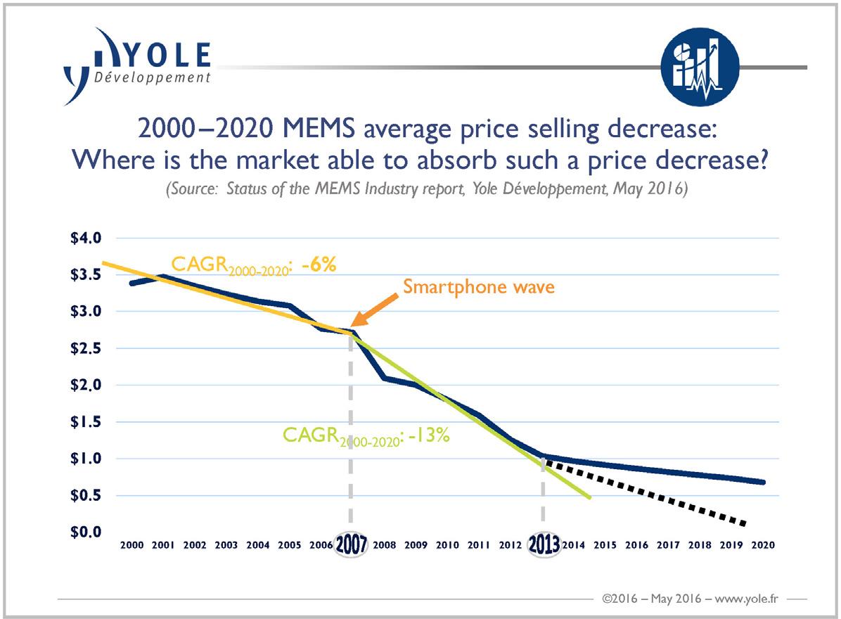
Foundriesservingthesemiconductorindustryhave increasinglyenteredintoMEMSvolumebusiness.As MEMSdevicemanufacturinghasdevelopedtoward CMOScompatibility,itispossibletoreuseagingsemiconductorlineswithaminimuminvestmentbarrier. DRIEtechnologyhaslargelyreplacedwetchemicalbulk micromachining,providingmorecommonalityintheprocessingofdifferentdevices,andmakingitpossibletofill the200mmmanufacturinglineswithreasonablenumber ofwaferstarts.Devicecostreductionspeedhasincreased, withfurtherpotentialforsignificantyearlycostreduction aspresentedin Fig.2
ApublicationandpatentanalysisreflectsthepreviouslypresenteddevelopmentoftheMEMSfield(Fig.3). Thepublicationvolumeshavebeenconstantlyrisingsince the1990sbuthavesaturatedoverallsincethemid-2000s. MEMSresearchhascontinuedtobestrong,buttherather constantyearlypublicationvolumessuggestthatthereis notahypetopicwithintheMEMSfieldnow.Itis notablethatalthoughpolymersubstratesandotheralternativestosiliconsubstrateshavebeenproposedfrequently [15,16],thenumberofstudieshasnotdeveloped substantially.Incontrast,opticalMEMSrepresentsan areaoflargeresearchactivitiesoverthelastcoupleof decadesand,inrecentyears,hashadmanynewapplicationsemergingbasedonthesedevices,aswillbediscussedlater.ThenumberofMEMSpatentshasincreased stronglysincethebeginningof2000,coincidingwiththe 19701990–20002005–152020–30
FIGURE1 FourwavesofMEMScommercialization.
WhereissiliconbasedMEMSheadingto?
FIGURE2 Averagesellingpricedevelopmentestimate2000 2020. ReprintedwithpermissionStatusoftheMEMSIndustryReport,Yole Developpement(Yole),2016ed. ,www.i-micronews.com . [14]
Number of patents
Number of p ublications
FIGURE3 BibliometricdataandpatentanalysisgeneratedfromtheScopusdatabase.Specifickeywordsearchstringswereusedingeneratingthe bibliometricdatabasefrom1990to2018.ThepatentdatawerelimitedtotheUSPatent&TrademarkOfficetoreducethenumberofmultipleresults duetopatentfamilies.
commercializationwaveofconsumerapplications.Still today,morepatentapplicationsaresubmittedyearly.So overall,thepublicationandpatentsituationinMEMS demonstratesanengineeringfieldthatontheonehand possessesarelativelyhighmaturityandhighpotentialfor newproductinnovationsandontheotherhandisstilla stronglydevelopingfield.
Morethan20yearsago,SensorsandActuatorsA, 1996issue1 2focusedonpapersonthefutureoutlookof MEMS.Whenlookingattheseforecaststoday,itcanbe statedthatauthorsmoreorlessunderestimatedthedevelopment.However,Ko [17] concludedintheissue,“From sensorsandactuatorstomicroelectromechanicalsystems (MEMS),tonanofabrication,smartmaterialsandsmart structures,thefutureofthefieldisunlimited.”Now,in 2019,thisstatementisstilltrue,andperspectivesareeven morepromisingthatforecastedinthepapersinthatissue. Differentscenarioshavebeenpresentedtoestimatethe futureglobalneedforsmartsensorsandactuators.Yole De ´ veloppement [18] estimatesthatthesemiconductor-
basedsensorsandactuatorsmarkettobe$100Bin2023 fromabout$50Bmarketin2018.PureMEMSmarket, excludingBAWdevices,willgrowfromabout$9.8B (2018)toaround$16Bin2023showinga9%annual growth(CAGR).Along-termscenariocouldturnouttobe moredramatic,iftheMEMSresearchcommunityand manufacturingindustrymanagetoutilizethestrengthsof thetechnologiesandtheinfrastructuresconsciouslyandto balancethechallenges.Inthefollowingparagraphs,some trendsandhigh-volumeopportunitiesarediscussedand reflectedwiththehelpoftheSWOTanalysis(Table1).
Newtechnologytrendsandemergingbusinessareas suchaslowcarbonsociety,autonomousdriving,AI, AR/VR,andIoTpresenthighdemandforcurrentandfurtherdevelopedversionsoftheexistingMEMSdevices. ThehypearoundIoTisstartingtoceaseanditisbecomingpartofoureverydaylife.ManyMEMStechnologies willbeonhighdemandtodevelopgridsofwirelesssensornodesthatcansenseandreportdetailedinformation amongeachotherandwiththeendusersforconcepts fromindustrialinsituhealthmonitoringandpredictive maintenancetosmarthomesandcities.Homeautomation offersevenasurprisinglyvirginplatformforhighperformanceandhighlyintegratedsensors.Asstand-alone
TABLE1 SWOTanalysisofMEMS.
Strengths
● SiliconMEMSdevicesarescalableindieandwafer size.costsdown
● BusinessstartstoresembleICbusiness:fablesscompanies, IDMs,foundries
● Miniaturizationpotentialstillsignificant
● Versatilityandvariabilityofthetechnology
● NewMEMSmanufacturingtechnologiesallowCMOS compatibility
● Strongresearchinfrastructurewithfablinesinseveralcountries
● R&Dfundingencouragingtocross-disciplinarycooperation quitewelldeveloped
Opportunities
● Newemergingbusinessareas:IoT,autonomousdriving,AI, andAR/VR
● NewconceptswithRFMEMS,optics,andMEMScombined, piezoactuation
● Newpackagingconcepts
● HybriddevicesintegratingMEMS,IC,energyharvestingand storage,RF
● Stillsignificantroomforcostreduction
● Significantpotentialforstartups,merge,andacquisition possibilities
● RoomfornationalandmultinationalR&Dfunding
● Newsoftwarebusiness,sensorfusion,anddecision-making
● Reuseopportunitiesfordesignswithlongdevelopmenttimes
devicessuchashomeappliances,lighting,andheating, venting,andairconditioningsystemswillbeintelligently connected,thesensorsinvolvedwillneedtomeasure multiplephysicalquantitieswithhighsensitivityandona constantbasis.Thesensormodulescanincludehuman tactilesensingandspecificwake-upfeaturesbasedon opticaldetection [19,20].Thiswillrequirelowpower ubiquitoussensorsintegratedwithMCUsandRFparts. AnotherexampleofnewapplicationsforexistingMEMS solutionswithinIoTisvoiceandgesturecontrol,which areexpectedtotakeoversmalltouchscreensandother controlpanelsinfuture.Here,microphoneorbetter microphonearray [21,22] isakeytoachievingoptimal performance.Voice-controlledsolutionswillbemost likelybasedonminiaturized,stableperformanceMEMS microphones,butalsotheyinvolvepotentiallyother MEMScomponentssuchasMEMSradarforspeakerdiarization [22].Tocopewiththeincreasingrequirements anddemandfordigitalMEMSmicrophonesandtoreduce parasiticsfromtheinterconnects,highdensity,even monolithicintegrationofthemicrophonechipandthe controlchip,isexpected.
Autonomouscarwillhaveextensiveimpactontechnologydevelopmentpushingthesensorperformance
Weaknesses
● Averageproductdevelopmentcycleslong
● Volumeperdevice/technologyremainslow,business prerequisitesoftennotmet
● Foundryservicesneedfurtherdevelopment
● Standardizationstillinearlystages,forexample,fewpin-to-pin compatibledevices
● “Yole’slaw”stilllimitsinsomedesignssecondsourcing
● Infrastructuralrenewalslow,componenttestingneeds specializedtools
● Researchfundingavailable,butlevelofchallengeslow,toofew projectsfailing
● Forceoutputlimitedforpotentialactuatorapplications
Threats
● Lackofcompetencewithmultidisciplinaryskills
● Delaysofnewdeviceintroductionsbecauseoldmilkcowsare notkilled
● Largecompaniesbasetechnologydevelopmenttoostrictlyon businesscases
● Companieslackingvisionorcourage
● Nofoundriescapableofofferingmanufacturingtosmall/ mediumscalevolumes
● Patenttrolls
● Architecturalchangesandendproductspecificationchanges removetheneed
● Designtimeandcostincreasingduetofunctionalsafetyand otherrequirements
AI,Artificialintelligence; AR,augmentedreality; IDM,Integrateddevicemanufacturer; IoT,Internetofthings; VR,virtualreality.
aheadinmanysegments.Forinstance,futurecarswillbe connectedalmostinrealtimetodifferentnetworks,with targetingtominimumlatencytimes,downto1ms [23] Toachievethis,servercentersneedtohavesatellitemini serversdistributedclosetocars.RFMEMSandoptical MEMSdevicesareneededtoachievenecessarylatency anddatavolume.Carswillcommunicatewithothervehicles,roadinfrastructureandcreatereal-timeperceptionof theenvironment.Thissituationawarenessiscreatedwith aidofmultitudeofsensors,andmanyofthoseareMEMS sensors.Toguaranteereliableinformation,thisperception willbecreatedwithindependentsensors.Thusinformationfromcamerasinvisualanduptofarinfraredrange areused,(scanning)radars,laserscanners,ultrasoundsensors,inertial(accelerometers,gyroscopes),temperature, andpressuresensorsarecombinedwithinformationgatheredwithradio.TheperformanceofthecurrentMEMS devicesneedstobeimprovedvastly,forexample,stabilityofthegyroscopeswithafactor10ormore [24]. Systemsbuildonsensorsneedtobefail-operational,fail safeisnotenough.Essentially,carwillbeinthefuturea movingfifth-generation(5G)(or6G)basestation.
Autonomouscarnotonlyreceivesanddigestinformationbutitcanalsosenddataformultitudeofpurposes.Car willbe,forexample,amovingweatherstationwhensendingdatatoinfrastructure.Thiswillmakeroadcondition monitoringandweatherforecastingmoreaccurateasthe measuringgridwillbedenseanddataactual.Inorderto processdataefficiently,new,advancedsoftwareisneeded; machinelearningandAIareplayingacentralrole.
AlsoalargepartoftheotherapplicationsofAI,many ofthemtargetingtoperformautonomouslyunstructured tasks,willrelyonsensor-generateddata.Muchof acquireddatawillbebasedoncommonMEMSsensor technologies,thoughwithimprovedaccuracy,higher sensitivity,andfasterresponsetime.FormatureMEMS technologies,thismeansdesignandspecification improvements,aswellasadvancedintegrationtocomputingandnetworkingdevices.Torealizetheseimprovements,progressisrequiredspecificallyinmanufacturing andintegrationmethods.Newinnovationsareexpected specificallyforopticalsensorapplications,suchasAIbasedfacialrecognitionusingathree-dimensional(3D) sensortomapauser’sface.Facialrecognitionandother optical3Dsystemsareexpectedtogrowtoa$1.5Bbusinessby2022 [25] withmuchofthelong-termgrowth potentialcomingoutsideofconsumerapplications. Advancedversionsof3Dopticalsensingwillrequirethe developmentoflightmanipulatingMEMSdevicesand theirintegrationwithlasersourcesanddiodereceiversin aminiaturizedopticalpackage.
ARandVRarenotonlyservingcreativeindustries suchasgaming,buttheyarealsoincreasinglyemerging intoindustrialdesign,real-estatebusiness,education,
healthcare,andmilitarynavigation.TheAR/VRbusiness hasbeenestimatedtogrowintoa$80Bmarketby 2025—hardwarerepresenting56%ofthevalue [26] Here,severaldifferenttypesofsensorsarerequiredfor the3Dimagevisualizationanduser’sinteractionsinthe environment.Highlysensitiveaccelerometersandgyroscopesareneededfortrackingofmovementandorientation,opticalandthermalsensorsareneededtoexplorethe surroundingsandlocateobjects.Similartoautonomous navigationforrobotics,progressinVRandARiscurrentlymainlydrivenbyalgorithmdevelopment.However, manynecessaryattributes,suchaslownoisemeasurementsandfastcommunicationtoaGPU,aredependent onfurtherdevelopmentsinMEMSandtheirintegration. Furthermore,projectionandimagealignmentforARwill requirenewopticalMEMSdevices,suchasmicromirrors.
MergingMEMSwithmicro-opticshasindeedopened upapromisingdirectionnowreemergingafteraninitial investmentboominthe2000s.Theminuteforcesneeded tosteerandmanagelightareidealforaMEMSactuator withlimitedforceoutputcapability.IntegrationofwaveguidesandMEMSallowsmodificationoflightpropagationinwaveguidesbymechanicalactuationandprovides opportunitiessuchasopticalswitches.Theearlyoptical MEMSdevelopmentworkdidnotleadtomanymarket entries,ascosttargetscouldnotbeachievedandcapacity ofthefiberlinescouldbeincreasedbyothermeans.But now,theemergingautonomousdrivingmaygiveanew opportunitytoMEMSmirrorsasseveralparallelimaging technologieswillbeused:cameras,radars,andlidars. Scanninglidarsareimagingdevicesbasedonpropagation andreflectionoflaserlightpulsesthataresteeredand collectedbyaMEMSmirror.Theremightbeanopportunitytopiezo-MEMSindrivingthemirrorstohighangularamplitudeatlowvoltage.
Besidestheautonomousdrivingandother3Dsensing applications,asignificantbusinessdriverisnowcloud computing [27].Datacentersneedmassivecomputing powerinhyperscaledatacenters,andthisisachieved withdirectopticalsignalswitchingandroutingforlarge reconfigurableall-opticalnetworksforfasttelecommunicationcapabilities.
Healthcaresegmentpresentsanothersignificant growthopportunityforMEMS.Healthcarecostinour agingsocietywillgrowtosignificantpartoftheGNP. Manynewgamechangersareneededtoreducedays spentinhospitals,preventiveandearlywarningmethods anddevicesfordiseases,betterandcheapermethodsand devicesfordiagnosisandtherapy.Minimuminvasivesystemshaveagoodpotentialtoreducecosts.RoboticsystemsandsmartcathetersrequirenewMEMSdevices suchasPMUTsandCMUTs(piezo-andcapacitively actuatedultrasoundsensors),forcesensors,pressuresensors,accelerometers,andgyroscopesthataresmall,
sensitive,stable,andreliable.MicrofluidicMEMSison riseforpoint-of-careandbedsidemedicaldiagnosis wheremicromanipulators,includingchannels,valves, pumps,andreservoirsaswellassensors,arerequiredto handle,transport,accuratelyrelease,andanalyzesmall volumesoffluid [28]
Noveldrugdeliverymethodshavebeenresearched intensivelyasMEMS-baseddevicescanprovideaccurate controlofthedosesandreleaserates [29,30].While thepromiseshavenotmaterializedsofarinalarge scale,therearesolutionssuchasminimallyinvasivetransdermalpatches,forexample,includingstimuli-responsive microneedles,whichcanbeseenaspotentialfor clinicalapplicationsinanearfuture [31].Ingeneral, implantablebiomedicalelectronicdevicescontaining MEMShavenotdiversifiedmuch,sinceapplicationssuch ascardiacpacemakerandMEMShearing-aidtransducer.It isexpectedthatcontinuousminiaturizationcombinedwith wirelesscommunicationmeanswillmakenewsubcutaneous implantspossible.Theprogresshasbeenslowmainlydueto thetightregulatorycontrolsforactiveimplantablemedical devices,butalsoduetosomeunsolvedbiocompatibility issues,specificallyincaseswherethesensoryelementsare exposedtobiologicalanalyte [32].
Wearablehealthmonitoringandwellbeingdevicesfor sportsandrecreationarebecomingincreasinglypopular foreverydayuse.Fitnesstrackers,smartwatches,oronepurposedevicessuchascufflessbloodpressuremeters areallloadedwithMEMSsensors.Newapproachesfor wearabledeviceshaverecentlybeingdeveloped [33] or areemerging—abletomonitorqualityofsleep,orto measureelectrocardiogram,atrialfibrillation,andlowand highheartratewithhighspecificityandsensitivity ( . 98%) [34].Alsointhesekindsofapplications,sensors relyheavilyonRF-communication.
Therealizationofthe5GmobilecommunicationsystemwillrequirenewRFcomponents,suchasRFfilters, switches,inductors,andvaractors.Itislikelythatmanyof thesecomponentsareintegratedonthesamedie.Siliconis astrongcandidateasasubstrate,althoughglassisalso usedinsomedesigns,especiallyinswitches.Newdevices areneededinbothhandsetsandbasestationsaswellasin backbonenetworks.Basestationsandhandsetswill employnewantennadesignshavingbeamformingcapability.TherewillbeneedforMEMSRFswitchesandtuners forantennaimpedancematching.Alsonewfiltersare needed;anexampleofnewFBARfilterisutilizinga hybridstructure,thinfilmlithiumniobateonsilicon,an SOI-likestructure [35].YoleDe ´ veloppementforecastsa growthfrom$2.4to15BforRFMEMS,includingBAW devicesin2023 [18].Substantialamountofresearchand developmentisstillneededinRFMEMSarea.
Piezoactuationofferscurrentlymanyunusedpossibilitiesfrommoreefficientinertialsensorstoenvironmental
energyharvesting.MEMSseemsanevidentcarrierto integratemechanicalenergyharvesters,whichcouldbe usedinpoweringsmall,long-lastingelectronicdevices suchasmeasurementequipmentinremoteorhostile environmentsandenableautonomous,self-sufficient wirelesssensornetworksforIoT.Differenttransduction mechanismshavebeenemployedandmuchresearchhas beendevotedtodesignMEMSresonatorswithsufficient amountofgeneratedpowerandcapableofadaptingthe frequencyleveltomatchtheambientvibrationfrequency. Here,miniaturizationpresentsatrade-offbetweenreductionofthepowerrequirementsofubiquitouselectronic devicesandincreasingoperatingfrequencyofthevibratingstructures.Recently,MEMSvibrationpowergeneratorshavebeenreportedtoyieldpowerdensitiesranging fromhundredsof µW/cm3 toseveralmW/cm3;someof themusingacombinationofmultipleenergyconversion mechanisms [36].Ifcombinedwithaneffectiveenergy storagesolution,suchasasupercapacitor,thisindicatesa leveluseableinpracticalapplicationsofwirelesssensor modules,includingRFcommunication.Still,thechallengeremainsontheusefulenergysourceastheresonancefrequencyoftheMEMSstructuresistypically muchhigherthanavailableenvironmentalvibration energy.Designfeaturestoincreaseproofmassandanchor structurestomaintainlinearbehaviorarethemaincountermeasurestoadaptthefrequency.
Thepreviouslyreviewedopportunitieswillrequire newhybridmaterialsolutionsandheterogeneousintegrationoftechnologies.Siliconwillcontinuetobethemain substratematerialforaverylongtime,butapartfromSi,a varietyofdifferentmaterialswillbeused,suchaspiezoelectricthinfilms,newwaferbondingmaterials,orprotectivecoatings,fortactilesensorsandimplantabledevices. However,theheterogeneousintegration,thustheMore thanMooreapproach,maycauseevenlargerchangeinthe manufacturinglandscapeinanearfuture.
Thecurrentstate-of-the-artMEMSintegrationstrategy isembeddedwafer-levelpackagingoreWLP(discussed inChapter33:Fan-outwafer-levelpackagingaspackagingtechnologyformicroelectromechanicalsystems). AlthoughthisapproachnicelyintegratesMEMSand CMOScomponentsintoasinglepackage,therearea numberoflong-termchallengesasdiesbecomethinner. First,thinnerdiesaremoresusceptibletoresidualstress effectsfromtheinherentcoefficientofthermalexpansion mismatches,suchasthemismatchbetweentheSi,dielectricandredistributionlayers,andsoldermaterial.In MEMSdevices,mechanicalstresswillcausedeterioration ofperformancemuchbeforeanytraditionalfunctional failureswilloccur.Second,therearetheassociatedimpurityproblemswithmoldingcompoundsthatpotentially resultindecreasedperformanceandfinallyincorrosionrelatedfailures.Thelong-termgoalshouldfocuson
eliminatingtheseissueswhileprovidingenhancedperformanceandhigherintegrationinasmallerpackage.In future,heterogeneouslyintegrateddevicechips,ICsand MEMS,areputinthepackagesidebysideorstacked resultinginhermeticallysealedmultichipstacks,different layersdedicatedfordifferentfunctions,forexample,for computing,sensing,energystorage,andcommunication.
Asdiscussed,sizereductionhasbeenakeyenablerto reducecostandhighvolumeproductionofMEMS. Continuedminiaturizationwillberequiredtoachievetrue ubiquitoussmartsystemsandmakeproductspossible, whichhavenotbeendoablesofar.PackagingandintegrationtechnologiesthatarecapableofprovidingsimultaneouslyhigherdegreeofMtMintegrationand miniaturizationneedtobeincreasinglybasedonmicrofabrication.Onesolutionmaybeanallsiliconpackage. Suchapackagehastheadvantageoflowerresidualstressesasabulkofthematerialissiliconwithareduced dependenceonmoldingcompoundsastheencapsulation isdonewiththesiliconitself.Inadditiontothisanallsiliconpackagecouldexploitsilicon-thinningprocesses,for ultrathinpackages,andtheadvancesofstandardCMOS processestoreduceprocessingcosts.Allsiliconpackage couldintegrateMEMSwithanaloganddigitallayers meaningnotonlythattheperformance,forexample, latencyandpowerconsumptionimprovesbutalsothe physicalpackageinterconnectswouldbelimited,thus reducingtheneedforfanningoutorevenallpackage interconnectswhatsoever.Anillustrationoftheallsilicon packagecanbeseenin Fig.4.Suchapackagewouldbe realizedbyasiliconwaferstackingprinciple,which wouldutilizeanumberofbondingtechniques.Multiple logiclayers,includingintegratedmemoryunits,couldbe stackedandintegratedusingthrough-siliconviaand fusionbondingtechnologies.Integratedsiliconpassive componentscouldbedesignedintothesiliconstack, removingtheneedforexternaldiscretedevices.Wafer bondingofmicrobumpsoftheembeddedpassivelayers
withredistributionlinescouldbeutilizedforChip-onWaferorWafer-on-Wafer.Finally,theMEMSsensorand actuatorintegrationcouldcompletetheautonomousor systemMEMS.AutonomousMEMSwouldbeafullsiliconcomponentthatisabletooperateasanindependent entity.Thehermeticallyencapsulatedsystemcouldbe implantedorembeddedanywherethusfurtherenabling ubiquitouselectronics.
Similarconceptideaswerebroughtupearlierby BSAC(BerkeleySensor&ActuatorCenter)atUC Berkeley.Thevisionarysmartdustprojectaimedtodemonstratethatacompletesensor/communicationsystem canbeintegratedintoamillimeter-scale“mote” [37]
Whensensorswillbeubiquitous,theimpactonsocietyandhumanbehaviorislargerthanwhenfixedline phoneswerereplacedwithmobilephonesconnectedin realtimetoInternet.Dronescanbescaleddowntoasize offleeusingMEMSmicromotors,otheractuators,and sensors.Accelerometersandgyroscopesputoneachfingernailcansensemotionandtransmitdata.Small(and cheap)sensorscanbeputinallpackages,forexample, foodtomonitortheconditionofthecontents. Applicationswouldbevirtuallyunlimited.Theresult wouldbewhatBryzekvisionedin2012whenhestarted theTrillionSensorsInitiativetosupportapathtoabundanceofsensors [38].Literally,allsocietalchallenges thattheglobalcommunityhastosolvearedirectlyor indirectlyrelatedtodevicesequippedwiththeabilitiesto detect,sense,andunderstandtheenvironmentandto makeoursurroundingsmoreresponsive,safer,and healthierwhileimprovingtheenergyefficiency.MEMS sensorsarenotchangingtheworldalone,buttheyhave synergisticeffectwithdevelopmentsinAI,VR/AR,and machinelearning.
ComingbacktotheSWOTanalysis(Table1),many thingsapartfromthetechnologiesaredecisivelyimportant tobeabletoturnthefutureopportunitiesintosuccessful businesses.Innovationshouldbestronglydrivenfrom
differentactors.Withanimprovedmanufacturinginfrastructure,smallcompanieshavebetterprospectstomove fastertovolumeproductioninafoundryinsteadneeding tobuildanewprocesslinetorealizetheidea.Still,availabilityofflexiblemanufacturinglinesabletoprovidesupportinthephaseofsmallandmediumvolume manufacturingwouldbehelpfultoreducethetimetomarketofnewproductconcepts.InnovationwithinlargercompaniesoftentakesplacethroughacquiringsmallerMEMS companieswithpromisingproducts,aswehaveseenin pastfewyears.Whilethiscanbeexpectedtocontinue, morerevolutionaryproductdevelopmentconceptsshould resultfromtheestablishedcompaniesownR&Dactivities.
Third-partyresearchfundingisinaveryimportant positiontofosterMEMSinnovation.Agoodamountof nationalandmultinationalresearchanddevelopment fundinghavebeenavailableinEuropeandotherareas stronginMEMS.Still,infutureinvestments,oneshould encouragetheapplicantstodevelopboldnewconcepts andplatformsinsteadofsupportingincrementalimprovements.WhileMEMSstillisinanearlydevelopment phase,bothtechnologyandindustrywise,itrequires morehighrisk,highchallengeprogramsdecliningprojectstargetingtobusiness-as-usual.
Furtheronthethreatsforthefuturedevelopmentof MEMS,detrimentaltotheadvancementoftheentire MEMSfieldisifriskavoidancestrategiesandprotection ofthecurrentlywellrunningproductsleadstohindering essentialdevelopmentsteps.Iflargecompaniestietechnologydevelopmentdecisionstoostrictlyonbusiness cases,alsotheirownrenewalisnottakingplace.Similar situationiscausedifastart-upcompanyisacquiredbya largecompanyjusttoceasethepromisingdevelopment forwhatcanbecalledartificialrespirationoftheexisting products.Visionaryengineersandmanagementare neededtotakefulladvantageoftheuniquepossibilities anddevelopMEMSbeyondlinearmarketandtechnology forecasts.AsSteveJobsissaidtostate,marketresearch maybeuseless,becausecustomersdonotknowwhat theywantuntilitisshowntothem.
Forfuturecompetitivecompaniesinthesemiconductorandelectronicsfield,theminiaturizedsmartsystem containingMEMSisaprospectivepathfordiversification,climbingupthevaluechainorupdatingtheirproductportfolio.Decisiveforthesecompaniesistobuild systemknowledge,thusapartfromtakingthefulladvantageofMEMStechnologies,oneneedstobeabletointegratethemefficientlywithothercomponents,power sources,RFcommunication,andembeddedsoftware.In multisensorsystems,thiswillalsoneedknowledgeof advancedsignalprocessingsuchassensorfusionmethodology [39] knowledgesothattheprocessingofsensorsignalscanpartiallyalreadybeimplementedonthe embeddedprocessor.
Ultimately,availablehumancapitalisthemostimportantsinglefactorforsuccess.Theinnovationswillbe generatedthere,wheretheuniversities,researchinstitutes, andsmallandlargecompaniesfindawaytonurturecompetencesandmultidisciplinaryskillswhichtheexciting MEMSandsmartsystem’sfieldrequires.
References
[1]PrimeFaradayPartnership:AnIntroductiontoMEMS. ,www. primetechnologywatch.org.uk.
[2] C.S.Smith,Piezoresistanceeffectingermaniumandsilicon,Phys. Rev.94(1953)42 49.
[3]A.D.Kurtz,J.Mallon,C.Gravel,KuliteSemiconductorProducts, ElectromechanicalTransducersandHousings,USPatent 3654579.
[4] H.C.Nathanson,R.A.Wickstrom,Aresonant-gatesiliconsurface transistorwithhigh-Qband-passproperties,Appl.Phys.Lett.7 (1965)84 86.
[5] K.E.Petersen,Siliconasamechanicalmaterial,Proc.IEEE70 (1982)420 457.
[6] H.Seidel,L.Csepregi,A.Heuberger,H.Baumgartel,Anisotropic etchingofcrystallinesiliconinalkalinesolutions,I.Orientation dependenceandbehaviourofpassivationlayers,J.Electrochem. Soc.137(1990)3612.
[7] H.Seidel,L.Csepregi,A.Heuberger,H.Baumgartel,Anisotropic etchingofcrystallinesiliconinalkalinesolutions,II.Influenceof dopants,J.Electrochem.Soc.137(1990)3626.
[8] F.Larmer,MEMSatBosch InventedforLife,IEEEMEMS, 2018,p.237.
[9] R.Bogue,RecentdevelopmentsinMEMSsensors:areviewof applications,marketsandtechnologies,Sens.Rev.33(4)(2013) 300 304.
[10]ITRS,WhitePaper“More-Than-Moore”.Availablefrom: ,http:// www.itrs2.net/uploads/4/9/7/7/49775221/irc-itrs-mtm-v2_3.pdf..
[11]Statista,Micro-ElectromechanicalSystems(MEMS)Market RevenuesWorldwideFrom2014to2024,byApplication(in MillionUSDollars).Availablefrom: ,https://www.statista.com/ statistics/796333/worldwide-mems-market-revenues-by-revenue/ . (viewed12.08.19).
[12]Statista,SemiconductorIndustrySalesWorldwide1987-2020. Availablefrom: ,https://www.statista.com/study/11803/globalsemiconductor-market-statista-dossier/ . (viewed12.08.19)
[13] E.Mounier,FutureofMEMS:AMarket&Technologies Perspective,MEMSTechSeminar,Milano,Italy,2014.
[14]StatusoftheMEMSIndustryReport,YoleDe ´ veloppement (Yole),2016ed. ,www.i-micronews.com.
[15] B.J.Kim,E.Meng,ReviewofpolymerMEMSmicromachining, J.Micromech.Microeng.26(2016)013001.
[16] C.Ge,E.Cretu,Asacrificial-layer-freefabricationtechnologyfor MEMStransduceronflexiblesubstrate,Sens.ActuatorsA286 (2019)202 210.
[17] W.Ko,Thefutureofsensorandactuatorsystems,Sens.Actuators A56(1996)193 197.
[18]StatusoftheMEMSIndustryReport,YoleDe ´ veloppement (Yole),2018ed. ,www.i-micronews.com.
[19] C.Chi,X.Sun,N.Xue,T.Li,C.Liu,Recentprogressintechnologiesfortactilesensors,Sensors18(2018)948.
[20] M.Sohgawa,A.Nozawa,H.Yokoyama,T.Kanashima,M. Okuyama,T.Abe,etal.,MultimodalMeasurementofProximity andTouchForcebyLight-andStrain-SensitiveMultifunctional MEMSSensor,IEEESensors,Valencia,Spain,2014.
[21] S.C.Lo,S.K.Yeh,J.J.Wang,M.Wu,R.Chen,W.Fang, BandwidthandSNREnhancementofMEMSMicrophonesUsing TwoPoly-SiMicromachiningProcesses,2018IEEEMicro ElectroMechanicalSystems(MEMS),Belfast,NorthernIreland, 2018.
[22] E.Zwyssig,SpeechProcessingUsingDigitalMEMSMicrophones (DoctoralDissertation),UniversityofEdinburgh,2013.
[23] I.Parvez,A.Rahmati,I.Guvenc,A.I.Sarwat,H.Dai,Asurvey onlowlatencytowards5G:RAN,corenetworkandcachingsolutions,IEEECommun.Surv.Tutor.20(2018)3098 3130.
[24]A.Torkkeli,MurataElectronicsOy,PersonalCommunication.
[25] M.Tagliavini,LightSensorsforConsumer&MobileReport,IHS Markit,2018.
[26] H.Bellini,W.Chen,M.Sugiyama,M.Shin,S.Alam,D. Takayama,Virtual&AugmentedReality:UnderstandingtheRace fortheNextComputingPlatform,GoldmanSachs,2016.
[27] M.Abu-Tair,P.Perry,P.Morrow,S.McClean,B.Scotney,G. Parr,etal.,Opticalspaceswitchesindatacenters:issueswith transportprotocols,Photonics6(2019)16.
[28] S.L.Karsten,M.C.Tarhan,L.C.Kudo,D.Collard,H.Fujita, Point-of-care(POC)devicesbymeansofadvancedMEMS, Talenta145(2015)55 59.
[29] H.J.Lee,N.Choi,A.S.Yoon,I.J.Cho,MEMSdevicesfordrug delivery,Adv.DrugDeliv.Rev.128(2018)132 147.
[30] F.Munoz,G.Alici,W.Li,Areviewofdrugdeliverysystemsfor capsuleendoscopy,Adv.DrugDeliv.Rev.71(2014)77 85.
[31] J.Yang,X.Liu,Y.Fu,Y.Song,Recentadvancesofmicroneedles forbiomedicalapplications:drugdeliveryandbeyond,Acta Pharm.Sin.B9(2019)469 483.
[32] B.D.Ratner,A.S.Hoffman,F.J.Schoen,J.E.Lemons(Eds.), BiomaterialsScience AnIntroductiontoMaterialsinMedicine, Elsevier:AcademicPress,2013.
[33] https://ouraring.com/
[34] https://support.apple.com/en-us/HT208955.
[35]T.Baron,E.Lebrassesur,F.Bassignot,H.Wang,S.Ballandras,J. Fan,etal.,WidebandlithiumniobateFBARfilters,Int.J. MicrowaveSci.Technol.2013(2013),articleID459767.
[36] J.Iannacci,Internetofthings(IoT);Internetofeverything(IoE); tactileInternet;5G a(notsoevanescent)unifyingvision empoweredbyEH-MEMS(energyharvestingMEMS)andRFMEMS(radiofrequencyMEMS),Sens.ActuatorsA272(2018) 187 198.
[37] https://www-bsac.eecs.berkeley.edu/programs/smartdust.html.
[38] J.Bryzek,R.Grace,Thetrillionsensorsinitiative,Commer. Micromanuf.Int.7(2014)42.
[39] S.Sarkka,BayesianFilteringandSmoothing,Cambridge UniversityPress,Cambridge,2013.
Chapter1
Propertiesofsilicon
MarkkuTilliandAtteHaapalinna OkmeticOy,Vantaa,Finland
1.1Propertiesofsilicon
SiliconisanabundantelementfoundintheEarth’scrustin variouscompounds.Worldwidepolysiliconproductionin 2017wasaround445,000twithamarketsizeofUS$6.5 billion.Mostofthesiliconisusedforphotovoltaicapplicationsandthequalityislowerthanthatrequiredinthe semiconductorindustry.Thesemiconductorgradesilicon productionusableforsemiconductorandmicroelectromechanicalsystems(MEMS)applicationswasaround 70,000t.TodaymostofthesiliconusediseitherN-or P-type,dopedwithantimony,arsenic,phosphorus(N-type), orboron(P-type);thedopantconcentrationrangesbetween 1013 and1020 dopantatoms/cm3 Si.Intrinsic(nointentional doping)orveryslightlydopedhighresistivitysiliconabove 1kΩ cmisusedinsmallamountsespeciallyinradiofrequency(RF)applications.Statisticspertainingtosilicon canbefound,forexample,inthe USGeologicalSurvey 2018MineralsYearbook [1,2]
Quartz,orsilicondioxide,isthemostcommonstartingrawmaterialforpurifiedsiliconforsemiconductor andsensorapplications,andtheSiemensprocessisthe mostcommonlyusedinsemiconductor-gradesiliconproduction.IntheclassicalSiemensprocess,metallurgicalgradesilicon,madefirstinanelectricarcfurnaceby reducingquartzwithcoke,isturnedtosilicon-hydrogenchloridecompoundsinfluidizedbedreactors,andthose compoundsareconvertedtoTCS(trichlorosilaneor SiHCl3).TCSispurifiedbydistillation,duringwhich concentrationsofimpuritycompoundshavingeithera lowerorhighertemperatureofvolatilitythanTCS (38.4 C)arereduced.PurifiedTCSisfedtogetherwith hydrogenintoareactor.Inthereactor,TCSdecomposes ontohotsiliconfilamentsformingapurepolysiliconrod. Thisrodisthenusedasarawmaterialforcrystalgrowth, eitherinrodformorincrushedpieces.Therearealternative,newertechniquesforpurifyingsilicon;onevariantis similartotheSiemensprocessbutusessilane(SiH4)asa precursor.Insomeprocesses,heatedsiliconfilamentsare
replacedbysiliconparticlesfloatinginfluidizedbedreactors;theseprocessesyieldgranularpolysilicon.
Theresultofthepurificationprocessishigh-puritysiliconcontainingverysmallamountsofforeigndissolved atoms.Ifthesinglecrystalsaremanufacturedbya Czochralski(CZ)technique,whichismostcommonly used(c90%ofthecrystals),theimpuritylevelincreases, asthegrowthismadefromaquartzcruciblehavingsome impurities.Theresultis,however,stillacceptable. Typically,mostofthecontaminationofthesilicontakes placeduringactualdevicemanufacturing.Ofimpurities, metalsaregenerallyharmful,withrareexceptions,and theirconcentrationshouldbeaslowaspossible,typically muchlessthan1012 atoms/cm3 Si.Oxygencomingfrom theCZ-crystalgrowthstepasanimpurityhasadualrole: ithasbeneficialeffects(strengtheningofthesiliconlatticeathightemperatures,getteringeffectinsemiconductoruse)butalsohasdetrimentaleffects(donorformation, defectgeneration).Nitrogenisasecondexampleofan impurity,anditcanbeusedinsmallquantitiestoenhance siliconproperties,especiallyin integratedcircuit(IC) applications.
Thecurrenthighdemandforlow-costsolar-gradesiliconencouragestheexploitationofalternativesourcesand newpurificationtechniques.Currently,thesemethodsare notabletoproducesemiconductor-gradesiliconpure enoughforMEMSapplications,althoughinsolarapplications,thesenewmethodsalreadyshowpromisingresults. WoditschandKoch [3] andIstratovetal. [4] listsomeof theavailablesolarsiliconpurificationtechniques.
SiliconisanidealmaterialforvariousMEMSapplications.Siliconisasemiconductorwhoseresistivitycanbe adjustedbydopingfromsub-mΩ cmtoseveralkΩ cm;it isquiteinertinanormalenvironment,hard,transparent inaninfraredregime,andelasticatroomtemperature withnoplasticdeformationandwithhighfracture strength.Finally,aprotectivestablesilicondioxidecan begrown.Siliconcrystalhasanisotropicproperties— mechanical,chemical,andelectrical—whichcanbe