FerroicMaterialsforSmartSystems
FromFundamentalstoDeviceApplications
JiyanDai
Author
Prof.JiyanDai
TheHongKongPolytechnicUniversity DepartmentofAppliedPhysics
HungHom
Kowloon
HongKong
Cover
©antoniokhr/GettyImages; (graph)CourtesyofProfessorJiyanDai, TheHongKongPolytechnicUniveristy
Allbookspublishedby Wiley-VCH arecarefullyproduced.Nevertheless, authors,editors,andpublisherdonot warranttheinformationcontainedin thesebooks,includingthisbook,to befreeoferrors.Readersareadvised tokeepinmindthatstatements,data, illustrations,proceduraldetailsorother itemsmayinadvertentlybeinaccurate.
LibraryofCongressCardNo.: appliedfor BritishLibraryCataloguing-in-Publication Data
Acataloguerecordforthisbookis availablefromtheBritishLibrary.
Bibliographicinformationpublishedby theDeutscheNationalbibliothek TheDeutscheNationalbibliotheklists thispublicationintheDeutsche Nationalbibliografie;detailed bibliographicdataareavailableonthe Internetat <http://dnb.d-nb.de>
©2020Wiley-VCHVerlagGmbH& Co.KGaA,Boschstr.12,69469 Weinheim,Germany
Allrightsreserved(includingthoseof translationintootherlanguages).No partofthisbookmaybereproducedin anyform–byphotoprinting, microfilm,oranyothermeans–nor transmittedortranslatedintoa machinelanguagewithoutwritten permissionfromthepublishers. Registerednames,trademarks,etc.used inthisbook,evenwhennotspecifically markedassuch,arenottobe consideredunprotectedbylaw.
PrintISBN: 978-3-527-34476-5
ePDFISBN: 978-3-527-81534-0
ePubISBN: 978-3-527-81537-1
oBookISBN: 978-3-527-81538-8
Typesetting SPiGlobal,Chennai,India PrintingandBinding
Printedonacid-freepaper 10987654321
Contents
1GeneralIntroduction:SmartMaterials,Sensors,and Actuators 1
1.1SmartSystem 2
1.2DeviceApplicationofFerroelectricMaterials 5
1.2.1PiezoelectricDeviceApplications 6
1.2.2InfraredSensor 7
1.2.3FerroelectricRAM(FeRAM) 8
1.3DeviceApplicationofFerromagneticMaterials 9
1.3.1Spin-TransferTorqueMemory 9
1.3.2MagneticFieldSensorBasedonMultiferroicDevice 9
1.4FerroelasticMaterialandDeviceApplication 10
1.5ScopeofThisBook 12 References 13
2IntroductiontoFerroelectrics 15
2.1WhatIsFerroelectrics? 15
2.1.1 P –E Loop 15
2.1.2RelationshipsBetweenDielectric,Piezoelectric,Pyroelectric,and Ferroelectric 16
2.1.2.1Ferroelectric–Dielectric 16
2.1.2.2Ferroelectric–Piezoelectric 17
2.1.2.3Ferroelectric–Pyroelectric 18
2.2OriginofFerroelectrics 18
2.2.1Structure-InducedPhaseChangefromParaelectricto Ferroelectric 18
2.2.2SoftPhononMode 19
2.3TheoryofFerroelectricPhaseTransition 21
2.3.1LandauFreeEnergyandCurie–WeissLaw 21
2.3.2LandauTheoryofFirst-OrderPhaseTransition 23
2.3.3LandauTheoryofaSecond-OrderPhaseTransition 26
2.4FerroelectricDomainsandDomainSwitching 28
2.4.1DomainStructure 28
2.4.2FerroelectricSwitching 28
2.5FerroelectricMaterials 29
2.5.1FromBaTiO3 toSrTiO3 29
2.5.2FromPbTiO3 toPbZrO3 32
2.5.3AntiferroelectricPbZrO3 33
2.5.3.1Pb(Zrx Ti1 x )O3 (PZT) 35
2.5.4RelaxorFerroelectrics 36
2.5.4.1RelaxorFerroelectrics:PMN-xPTSingleCrystal 37
2.5.4.2PolarNanoRegions 38
2.5.4.3MorphotropicPhaseBoundary(MPB)ofPMN-PTCrystal 40
2.6FerroelectricDomainandPhaseFieldCalculation 41 References 42
3DeviceApplicationsofFerroelectrics 47
3.1FerroelectricRandom-AccessMemory 47
3.2FerroelectricTunnelingNon-volatileMemory 50
3.2.1TunnelingModels 51
3.2.2Metal–Ferroelectric–SemiconductorTunnelJunction 55
3.2.3FerroelectricTunnelingMemristor 56
3.2.4StrainModulationtoFerroelectricMemory 57
3.3PyroelectricEffectandInfraredSensorApplication 58
3.3.1PyroelectricCoefficient 58
3.3.2PyroelectricInfraredSensor 59
3.3.3PyroelectricFiguresofMerit 60
3.4ApplicationinMicrowaveDevice 63
3.5FerroelectricPhotovoltaics 65
3.6ElectrocaloricEffect 67
References 68
4FerroelectricCharacterizations 73
4.1 P –E LoopMeasurement 73
4.2Temperature-DependentDielectricPermittivityMeasurement 76
4.3PiezoresponseForceMicroscopy(PFM) 77
4.3.1ImagingMechanismofPFM 77
4.3.2Out-of-planePolarization(OPP)andIn-planePolarization(IPP) PFM 80
4.3.2.1ElectrostaticForceinPFM 83
4.3.2.2PerspectivesofPFMTechnique 84
4.4StructuralCharacterization 86
4.5DomainImagingandPolarizationMappingbyTransmissionElectron Microscopy 87
4.5.1SelectedAreaElectronDiffraction(SAED) 88
4.5.2ConvergentBeamElectronDiffraction(CBED)forTetragonality Measurement 91
References 92
5RecentAdvancesinFerroelectricResearch 95
5.1SizeLimitofFerroelectricity 95
5.2FerroelectricityinEmerging2DMaterials 96
5.3FerroelectricVortex 99
5.4MolecularFerroelectrics 104
5.5FerroelectricityinHfO2 andZrO2 FluoriteOxideThinFilms 106
5.6FerroicPropertiesinHybridPerovskites 114 References 117
6PiezoelectricEffect:BasicTheory 123
6.1GeneralIntroductiontoPiezoelectricEffect 123
6.2PiezoelectricConstantMeasurement 124
6.2.1PiezoelectricChargeConstant 125
6.2.2PiezoelectricVoltageConstant 126
6.2.3DielectricPermittivity 127
6.2.4Young’sModulus(ElasticStiffness) 127
6.2.5ElasticCompliance 127
6.2.6ElectromechanicalCouplingFactor 128
6.2.6.1HowtoMeasureElectromechanicalCouplingFactor? 129
6.3EquivalentCircuit 132
6.4CharacterizationofPiezoelectricResonatorBasedonaResonance Technique 135
6.4.1LengthExtensionalModeofaRod 135
6.4.2ExtensionalVibrationModeofaLongPlate 138
6.4.3ThicknessShearModeofaThinPlate 139
6.4.4ThicknessModeofaThinDisc/Plate 140
6.4.5RadialModeinaThinDisc 141
6.4.6MechanicalQualityFactor 141 References 141
7PiezoelectricDevices 143
7.1PiezoelectricUltrasonicTransducers 143
7.1.1StructureofUltrasonicTransducers 143
7.1.2TheoreticalModelsofUltrasonicTransducer(KLMModel) 145
7.1.3CharacterizationofUltrasonicTransducers 147
7.1.3.1Bandwidth(BW) 147
7.1.3.2SensitivityoftheTransducer 148
7.1.3.3Resolution 148
7.1.4TypesofUltrasonicTransducers 149
7.1.4.1MedicalApplication 149
7.1.5PiezoelectricFilmApplicationinUltrasoundTransducers 149
7.1.6ChallengesandTrendofDevelopingNewAdvancedUltrasound Transducers 150
7.2UltrasonicMotor 150
7.2.1Terminologies 151
7.2.2DesignofUSM 153
7.3SurfaceAcousticsWaveDevices 154
7.3.1InterdigitalElectrodeinSAWDevice 155
7.3.2AcousticWave 155
7.3.3PiezoelectricPropertyConsiderationsforSAWDevices 157
7.3.4CharacterizationofSAWDevices 159
7.3.5Lead-FreePiezoelectricMaterials 161 References 163
8Ferromagnetics:FromMaterialtoDevice 165
8.1GeneralIntroductiontoFerromagnetics 165
8.2FerromagneticPhaseTransition:LandauFree-EnergyTheory 168
8.3DomainandDomainWall 169
8.4MagnetoresistanceEffectandDevice 171
8.4.1AnisotropicMagnetoresistance(AMR) 171
8.4.2GiantMagnetoresistance(GMR) 172
8.4.3ColossalMagnetoresistance(CMR) 175
8.4.4TunnelingMagnetoresistance(TMR) 176
8.4.4.1Spin-TransferTorqueRandom-AccessMemory(STT-RAM) 177
8.5MagnetostrictiveEffectandDeviceApplications 178
8.5.1MagnetostrictivePropertiesofTerfenol-D 180
8.5.2MagnetostrictiveUltrasonicTransducer 183
8.5.3MagnetoelasticEffect 184
8.5.3.1MagnetomechanicalStrainGauge 185
8.6CharacterizationsofFerromagnetism 186
8.6.1VibratingSampleMagnetometer(VSM) 186
8.6.2SuperconductingQuantumInterferenceDevice(SQUID) 187
8.6.3MagneticForceMicroscopy(MFM) 188
8.6.4Magneto-OpticalKerrEffect(MOKE) 189
8.7HallEffect 191
8.7.1OrdinaryHallEffect 191
8.7.2AnomalousHallEffect 191
8.7.3SpinHallEffect 192 References 193
9Multiferroics:SinglePhaseandComposites 197
9.1IntroductiononMultiferroic 197
9.2MagnetoelectricEffect 199
9.3WhyAreTheresoFewMagneticFerroelectrics? 199
9.4SinglePhaseMultiferroicMaterials 200
9.4.1SwitchingMechanisminBFOFilms 204
9.5MECompositeMaterials 205
9.6ModelingtheInterfacialCouplinginMultilayered METhinFilm 207
9.6.1PZT/CFOMultilayeredHeterostructures 207
9.6.2FerroelectricPropertiesofPZT/CFOMultilayers 209 References 212
10DeviceApplicationofMultiferroics 217
10.1MECompositeDevices 217
10.1.1EffectofPreloadStress 221
10.2MemoryDevicesBasedonMultiferroicThinFilms 223
10.3MemoryDevicesBasedonMultiferroicTunneling 224
References 229
11FerroelasticityandShapeMemoryAlloy 231
11.1ShapeMemoryAlloy 231
11.1.1SMAPhaseChangeMechanism 232
11.1.2NonlinearityinSMA 233
11.1.3One-WayandTwo-WayShapeMemoryEffect 235
11.1.4SuperelasticEffect(SE) 235
11.1.5ApplicationExamplesofSMAs 236
11.2FerromagneticShapeMemoryAlloys 237
11.2.1FormationofTwinVariants 238
11.2.2ChallengesforNi–Mn–GaSMA 242
11.2.3DeviceApplicationofMSMA 243
References 244
Index 247
GeneralIntroduction:SmartMaterials,Sensors,and Actuators
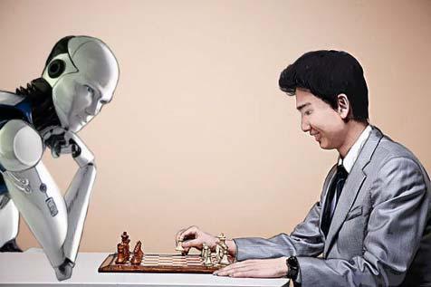
Theearlytwenty-firstcenturyhasforeseenaccelerationofinnovationsin roboticsandautomationsaswellasartificialintelligence(AI),wheresensors/ transducersandsmartmaterialsplayveryimportantroles.TheconceptofAI hasbeenaroundsincethelate1950s;however,it’sonlysincethefirstdecadeof thetwenty-firstcenturythatexcitementaboutithasreallybeguntogrowdue totheabilityoffastcomputationandabundantsizeofmemorydevices.Avery successfuldemonstrationofAIisGoogle’sAlphaGo,whichisthefirstcomputer programtodefeataprofessionalhumanGoplayer(seeFigure1.1).Another successfulapplicationofAIistheunmannedvehiclesandaircraftswherelarge numberofsensorsandactuatorsareused.
Onemayask,whatistherelationbetweenthekeyword“ferroicmaterials”of thisbookandthementionedrobotics,automations,andAI?Theansweristhat thesesmartandintelligencesystemsrelyonlargeamountofdatafromsensors andmemoriesformachinelearningandactuatorsforclose-loopedfeedbackcontrolsystems;andamongthesesensors,actuators,andmemories,ferroicmaterials playveryimportantroles.
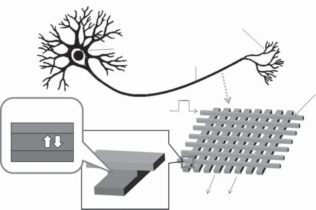
Forexample,thepiezoelectricpropertyofaferroelectricmaterial(oneofthe mosttypicalferroicmaterials)canbeusedforultrasoundsensorstodetectdistanceofyourcarfromawallforautoparkingsystem.Aferroelectricmaterialcan beusedasthefunctionalelementformanykindsofsensorsfrompressuresensor toaccelerationsensor,infraredsensor,etc.Beyondthat,aferroelectricpolarizationanditsswitchingcanalsobeusedinmemorydevicessuchasferroelectric random-accessmemory(FeRAM)wheretheferroelectriclayeractsasgateinsulatorinafield-effecttransistor(FET)structure.Ferroelectrictunneling-based resistiverandom-accessmemory(RRAM)hasalsobeendemonstrated,andsuch ferroelectric-basedmemoryhasbeenshowntobeabletoperformasanartificial synapse.Moreinterestingly,artificialneuralnetworks(ANNs)basedonthese ferroicsynapsescanrealizebrain-likecomputingandAIfunctionssuchasimage recognition.AsshowninFigure1.2,synapseswithBiFeO3 (BFO)ferroelectric layerhasbeensuccessfullydemonstrated.
Thisbookwilltellyoufundamentalsandcharacterizationmethodsofferroic materials,physics,andtechnologiesbehindferroicdevicedesignandapplicationsaswellastheirrecentadvances.
FerroicMaterialsforSmartSystems:FromFundamentalstoDeviceApplications, FirstEdition.JiyanDai. ©2020Wiley-VCHVerlagGmbH&Co.KGaA.Published2020byWiley-VCHVerlagGmbH&Co.KGaA.
2 1GeneralIntroduction:SmartMaterials,Sensors,andActuators
Figure1.2 Across-barstructureofsynapseandartificialneuronnetworksbasedona cross-barstructure.FerroelectricthinfilmssuchasBiFeO3 canbeusedasthejunctionmaterial. Source:AdaptedfromBoynetal.(2017).
1.1SmartSystem
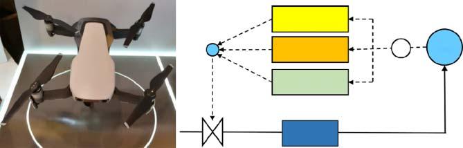
Asmartsystem,suchasaself-drivingcarorremote-controlaircraft,isasystemthatreliesonsensorsandactuatorstorealizeinstantfeedbackofcontrolled variables(CVs)suchasspeed,height,etc.Thebasiccomponentofasmartsystemusuallycontainssensors,actuators,andcontrolsystem.Anintelligentsmart systemneedslargeamountofdataprocessingandmemories,whileferromagneticandferroelectricmaterialshavebeenimplementedinrealizingnon-volatile memristors.Beyondthat,memoriesbasedonferroelectricthinfilmsmayalso findapplicationinelectronicsynapsesasbuildingblockstowardbuildingANN.
Figure1.1 AIbeatshumanchessplayer.
Nucleus
Axon
Axon
Synapse
Figure1.3 (a)Photoofaremotecontrolcopterand(b)diagramofaPIDfeedbackcontrol systemwheresensorsandactuatorsareimplemented.
Asanexample,asmartsystemofremotecontrolcopterrelyingon proportional–integral–derivative(PID)feedbackcontrolsystemisshown inFigure1.3.PIDisathree-orderfeedbackcontrolsystemthathasbeenwidely usedinautodrivingvehiclesandauto-pilotairplanestomakethedynamic systemoperatesmoothlyorbeingstableduringvideoimaging.Equation(1.1) illustratesthemechanismofPIDcontrolwherethreetermsofproportionalgain (P),integralgain(I),andderivativefeedback(D)canprovideinstantresponseto curetheerror(E)betweenthesetpoint(speedofvehicleorheightofthecopter) andcontrolledvariable(CV):
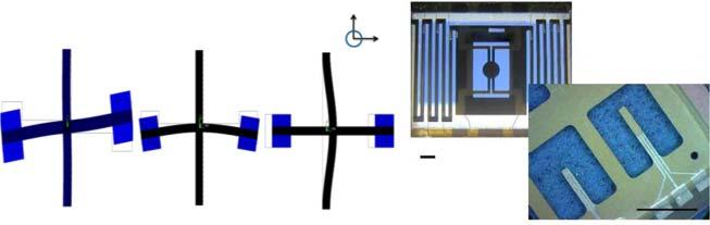
Inthisfeedbackcontrolsystem,wecanfindapplicationsofferroicmaterials,for example,piezoelectric-basedgyroscope,surfaceacousticwavedeviceforwireless communication,andferroelectric-basedinfrareddetector.Ingyroscope,rotation andaccelerationcanbesensedbymeasuringinducedvoltagegeneratedbypiezoelectriceffect;asurfaceacousticwavedevicebasedonpiezoelectriceffectisused forcommunicationbandselection;andaferroelectric-basedinfrareddetector canbeusedasanintrudersensormakingthecopterabletofindpeopleforrescuemission.Figure1.4showsthefiniteelementmodeling(FEM)simulationof threeresonantmotionsinaPb(Zrx, Ti1 x )O3 (PZT)-basedgyroscopeandphoto ofafabricatedgyroscope(ChangandChen2017).
Sensors:Devicesthatcan“sense”achangeinsomephysicalcharacteristicsand performanelectricalinputfunctionarecommonlycalled sensors.Forexample, astrainsensorconvertsmechanicalstrainintoelectricalsignal.
Actuators:Devicesthatperformanoutputfunctionaregenerallycalled actuators.Anactuatorcanbeutilizedtocontrolsomeexternalmodulioroutput mechanicalmovementsuchasultrasonicwave.Forexample,anatomicforce microscope(AFM)usespiezoelectricactuatorstorealizescanningalongthree directions.
Transducers:Bothsensorsandactuatorsarecollectivelyknownas transducers becausetheyareusedtoconvertenergyofonekindintoenergyofanother kind.Transducerscanbeusedtosenseawiderangeofdifferentenergyforms
1GeneralIntroduction:SmartMaterials,Sensors,andActuators
Figure1.4 FEMsimulationsofthreeresonantmotionsinaPZT-basedgyroscopeandphotoof afabricatedgyroscope.Source:AdaptedfromChangandChen(2017).
suchasmovement,electricalsignals,thermalormagneticenergy,etc.Thetype ofinputoroutputtransducersbeingusedreallydependsonthetypeofsignal orprocessbeing“sensed”or“controlled,”butwecandefineatransducerasa devicethatconvertsonephysicalquantityintoanother.
Asmartsystemneedssensorsandactuatorstorealizethesensingfunctions suchasdistance,movement,andaccelerationaswellasactions.Thesesensors andactuatorsusesmartmaterialstorealizetheconversionbetweendifferent energiesandmodulitoelectricalsignalssuchasvoltage,current,andcapacitance.Ofcourse,manysensordevicesaremadeofsemiconductorssuchasthe FET,butthisisnotthefocusofthisbook.
“Smartmaterial ”isaverylargeconcept,infact,thereisnostupidmaterial(a joke),i.e.allmaterialsaresmartinsomewaysincetheyallhavetheirownpropertiesandresponsetoexternalstimuli.Butinthisbook,werestrictthe“smart materials”tothosematerialswith“ferroic”characteristics.Wefocusonbasic physics,materialsscience,structures,devices,andapplicationsofferroicmaterialsforsmartsystems.Theferroicmaterialsareusuallyclassifiedaspossessing oneofthefollowingsbasedoncouplingofstimuli:
(i) Ferroelectric,whichisalsopiezoelectricwhenelectromechanicallycoupled andpyroelectricwhenthermoelectricallycoupled.
(ii) Ferromagnetic,whichisalsomagnetostrictivewhenmagnetomechanically coupled.
(iii) Ferroelastic,whichalsoincludesshapememorywhenthermomechanically coupled.
Amongtheseferroics,wecanseethatstrain,electricpolarizationandmagnetization,andtheirinterplayorcouplingareinvolved.Wecallamaterialasferroic materialifitpossessesatleastoneofthepropertiesofferroelectric,ferromagneticandferroelastic.
IfwelookatthediagramshowninFigure1.5,wecanseethatthecoupling andinterplaybetweenelectricity,mechanics,magnetism,heat,andopticsresult inmanysmartfunctions,suchasferroelectric,piezoelectric,pyroelectric,ferromagnetic,electromechanical,etc.Onebookcannotcoverallofthem,butthose belongtoferroicmaterialsanddevicesespeciallyintheformofthinfilmswillbe
1.2DeviceApplicationofFerroelectricMaterials 5
Figure1.5 Diagramshowingcouplingbetweendifferentmoduliandtheclarificationofsmart materials.
extensivelyintroducedinthisbook.Beforegoingintodetails,someapplication examplesofferroicmaterialsinsmartsystemsaregiveninthischapter.
1.2DeviceApplicationofFerroelectricMaterials
Whenpeopletalkaboutapplicationsofferroelectricmaterials,thefirstthing jumpsoutismostpossiblythePZT(lead–zirconium–titanatewithchemical formulaPb(Zrx Ti1 x )O3 ),whichisknownasanexcellentpiezoelectricmaterial. Asthemostpopularferroelectric,PZTisalsothemostimportantpiezoelectric materialincommercialapplications.Piezoelectricmaterialshaveverybroad applicationsinmanyfields,frommedicalultrasoundimagingtoultrasonic wirebondingmachineinsemiconductorindustry,frompressuresensorsto accelerometer,etc.ThemarketsizeofpiezoelectricmaterialsismorethanUS $1billionnowandisexpectedtobeUS$1.68billionby2025(GRANDVIEW RESEARCH).
Anotherfieldofapplicationofferroelectricmaterialsistheinfraredsensors basedontheirpyroelectricproperty,whichisalsooneofthemostimportant propertiesofaferroelectricmaterial.Beyondthesewell-knownapplications, anotherimportantapplicationbasedontheswitchingofferroelectricpolarizationisthenon-volatilememorydevicesuchasFeRAM.Examplesaregivenin thefollowinganddetailswillbeintroducedinthefollowingchapters.
1.2.1PiezoelectricDeviceApplications
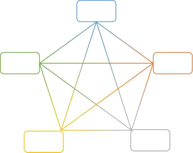
Anexampleofsmartsystemusingpiezoelectricmaterialisthedistanceradar systeminacarorasonarsysteminsubmarinesasshowninFigure1.6,wherethe keysensingelementisbasedonpiezoelectricmaterialtorealizetheconversion betweenelectricalenergyandacousticenergyforsendingandreceivingsound waves.Otherapplicationexamplesofpiezoelectricdevicesincludeactivedampingsystem,micro-scanningsysteminscanningprobeimaginginstrument(such asAFM),forcesensor,accelerometer,energyharvesting,etc.
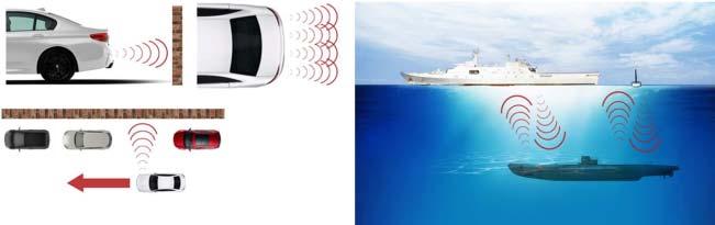
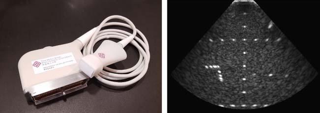
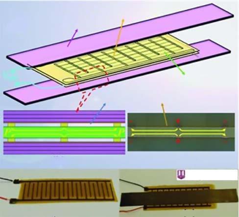
Medicalultrasoundimagingsystemwithpiezoelectricmaterialasthetransducertoconvertelectricalandacousticenergiesisanotherverygoodexample ofdeviceapplicationwherethepiezoelectricmaterialplaystherolesofsensingandactuatingfunctions.Figure1.7showsphotosofultrasoundtransducers developedinourgroup.Knowledgeinultrasoundtransducerfabrication,characterization,andapplicationswillbeintensivelyintroducedinChapter6.
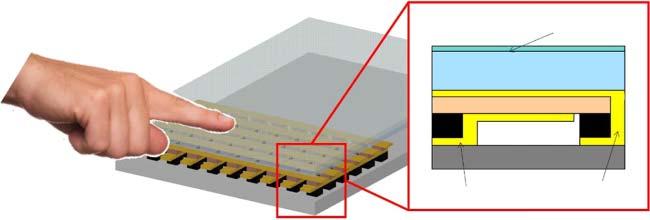
Averynewapplicationexampleispiezoelectric-basedfingerprintIDsystemin mobilephone.Thecurrentlyusedfingeridentificationsystemisbasedoncapacitancemeasurementtoobtaintwo-dimensional(2D)informationoffingerprint, butitfacestheproblemofdifficultytoidentifythefingerprintwhenthefingeris dirtyorwet.Ultrasoundfingerprintidentificationsystembasedonpiezoelectric ultrasonictransducerandimagingsystemcanobtainathree-dimensionalimage
Figure1.6 Piezoelectricmaterials-basedsonarsystemforcar(a)andsubmarine(b).
(a)
(b)
Figure1.7 (a)Transducersand(b)B-modeimageofawirephantomacquiredwith PolyU-madearrayultrasoundtransducer.
(b)
(a)
1.2DeviceApplicationofFerroelectricMaterials 7
PMUT unit
Capping layer
Coupling materials + MEMS
Piezoelectric layer
Cavity
CMOS wafer
Bottom electrodeTop electrode
Figure1.8 Illustrationofconceptofaultrasonictransducer-basedfingerprintIDsystembased oncomplementarymetal-oxide-semiconductormicro-electro-mechanicalsystems (CMOS-MEMS)technology.
offingerprintwithacertaindepth.Thiscanovercometheproblemsofthecurrentfingerprintidentificationsysteminmostmobilephones.InvenSense,Inc.is oneofthemainsuppliersofthissolution,andFigure1.8isanillustrationofthe ultrasonicfingerprintsystem.
1.2.2InfraredSensor
Aninfraredsensorisusuallymadeofaferroelectricmaterial,whichisalso pyroelectricthatgeneratessurfaceelectricchargeswhenexposedtoheat intheformofinfraredradiation.Apyroelectric-basedinfraredsensorcandetect thetemperaturechangebutproducenoresponseforasteadytemperaturesince thepyroelectricsensingelementcanonlyproducepolarizationchange-induced electricchargewhenthesensorissubjecttotemperaturechange.Figure1.9a showsaphotoofarealinfrareddetectorwithitsinternaldevicestructure illustratedinFigure1.9b,wheretheactiveelementismadeofpyroelectric materialssuchasLiTaO3 .Thosepyroelectricmaterialswiththeirpolarization abletobeswitchedareferroelectrics.Therefore,pyroelectricsensorsthatare widelyusedasinfrareddetectorsareimportantdeviceapplicationsforferroic materialsinasmartsystem.
electrode layer
Circuit board
(a)(b)
Figure1.9 Aphotoofaninfrareddetector(a)andillustrationofitsinternalstructure(b).
Window
Pyroelectric plate
Bottom electrode
Absorbing
1.2.3FerroelectricRAM(FeRAM)
FerroelectricRAM(FeRAM,F-RAM,orFRAM)isarandom-accessmemorythat issimilartoDynamicRandomAccessMemory(DRAM)instructurebutusesa ferroelectriclayerinsteadofadielectriclayertoachievenon-volatility.FeRAM isoneofagrowingmemberofalternativenon-volatilerandom-accessmemory technologiesthatoffersthesamefunctionalityasflashmemory.
AdvantagesofFeRAMoverflashmemoryincludelowerpowerusage,faster writeperformance,andmuchgreatermaximumread/writeendurance(about 1010 –1014 cycles).FeRAMshavedataretentionofmorethan10yearsat +85 ∘ C (uptomanydecadesatlowertemperatures).MarketdisadvantagesofFeRAM aremuchlowerstoragedensitiesthanflashdevicesandhighercost.
Aferroelectricmaterialhasanonlinearrelationshipbetweentheappliedelectricfieldandthestoredcharge.Specifically,theferroelectriccharacteristichas theformofahysteresisloop,whichisverysimilarinshapetothehysteresis loopofferromagneticmaterials.Thedielectricconstantofaferroelectricistypicallymuchhigherthanthatofalineardielectricbecauseoftheeffectsofelectric dipolesformedinthecrystalstructureoftheferroelectricmaterial.Whenan externalelectricfieldisappliedacrossadielectric,thedipolestendtoalignthemselveswiththefielddirection.Thisalignmentprocessisproducedbysmallshifts inthepositionsofionsandshiftsinthedistributionsofelectricchargesinthe crystalstructure.Afterthechargesareremoved,thedipolesretaintheirpolarizationstate.Binary“0”sand“1”sarestoredasoneofthetwopossibleelectricpolarizationsineachdatastoragecell.Forexample,inFigure1.10,a“1”isencoded usingthenegativeremnantpolarization“ P r ,”anda“0”isencodedusingthepositiveremnantpolarization“+P r ”.InthisFETstructurewithaferroelectriclayeras gatedielectric,thetwopolarizationstatescorrespondtodifferent V th ,resulting inamemorywindowwithinwhichtheONandOFFstatesoftheFETcanberead.

Figure1.10 Schematicdiagramoffield-effecttransistor(FET)andthecurrent–voltage(I–V ) characteristicsinducedbytwodifferentpolarizationstate.
1.3DeviceApplicationofFerromagneticMaterials 9
FeRAMremainsarelativelysmallpartoftheoverallsemiconductormarket. In2016,worldwidesemiconductorsaleswereUS$338.93billion(accordingto WSTS,SIA),withtheflashmemorymarketaccountingforUS$59.2billion (accordingtoICinsights(Cho2018)).The2017annualrevenuegrowthof Cypresssemiconductor,perhapsthemajorFeRAMvendor,werereportedto beUS$2.33billion.Themuchlargersalesofflashmemorycomparedwiththe alternativeFeRAMssupportamuchlargerresearchanddevelopmenteffort. Flashmemoryisproducedusingsemiconductorlinewidthsof15nmatRenesas ElectronicsCorporation(2017).Flashmemorycanstoremultiplebitspercell (currentlySamsunghasannouncedthe64-layer512-GbintheNANDflash devices).Asaresultofinnovationsinflashcelldesign,thenumberofbitsper flashcellisprojectedtoincreasetodoubleoreventotriple.Asaconsequence, thearealbitdensitiesofflashmemoryaremuchhigherthanthoseofFeRAM, andthusthecostperbitofflashmemoryisordersofmagnitudelowerthanthat ofFeRAM.
1.3DeviceApplicationofFerromagneticMaterials
Amongmanysuccessfulapplicationsofferromagnetic-baseddevices,memory devicebasedonferromagneticmaterialisoneofthemostsuccessfulexamples, especiallyinthethinfilmform.Thisismanifestedbytheverylargemarketof magneticharddiscincomputingsystems.Butinmostrecentyears,solidstate memory(mainlyflashmemory)issupersedingthemagneticharddisc.Nevertheless,ferromagneticmaterialalsofindsitsapplicationinnon-volatilememories suchasspin-transfertorquememory.
1.3.1Spin-TransferTorqueMemory
Spin-transfertorquecanbeusedtofliptheactiveelementsinmagnetic random-accessmemory.Spin-transfertorquemagneticrandom-accessmemory (STT-RAMorSTT-MRAM)hastheadvantagesoflowerpowerconsumption andbetterscalabilityoverconventionalmagnetoresistiverandom-accessmemory(MRAM),whichusesmagneticfieldtofliptheactiveelements.Spin-transfer torquetechnologyhasthepotentialtomakepossibleMRAMdevicescombining lowcurrentrequirementsandreducedcost;however,theamountofcurrent neededtoreorientthemagnetizationatpresentistoohighformostcommercialapplications,andthereductionofthiscurrentdensityaloneisthebasis forpresentacademicresearchinspinelectronics.Figure1.11isaschematic diagramofspinvalvestructure,whilearrowsindicatethemagnetization direction.
1.3.2MagneticFieldSensorBasedonMultiferroicDevice
Ifamaterialpossessesmorethanoneoftheferroicpropertiesofferroelectric, ferromagneticandferroelastic,itiscalledmultiferroics.Unfortunately,such
1GeneralIntroduction:SmartMaterials,Sensors,andActuators
Figure1.11 Schematicdiagramofspinvalvestructurewherearrowsindicatethe magnetizationdirections.
materialsarerareandareusuallystronginonepropertybutveryweakin another,suchasBiFeO3 ,whichisverystronginferroelectricsbutveryweakin ferromagnetic(itisantiferromagneticinfact).Thismakesmultiferroicmaterials hardtobepracticallyappliedindevices.However,peoplehavebeentryingto makecompositematerialssuchaspiezoelectricwithmagnetostrictivematerials,wherethemechanicalcouplingbetweenthemmakesthe“multiferroic” meaningfulfordeviceapplication,forexample,makingverysensitivemagnetic fieldsensor.
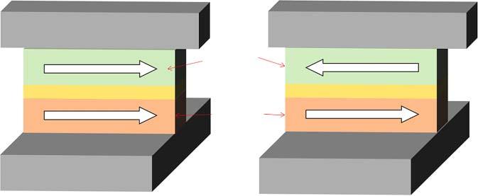
Themagnetoelectric(ME)effectisthephenomenonofinducingmagnetizationbyanappliedelectricfield(E )orpolarizationbymagneticfield(H ).Many effortshavebeendevotedtoimprovethelimitofdetectionoftheMEcompositeatlowfrequencyrange,andvaluesof ∼10 7 Oeat1Hzhasbeenreported (Wangetal.2011).Basedonthemagnetic–strain–electriccoupling,scientists havedemonstrateddcmagneticfieldsensorwithadetectionlimitof2 × 10 5 Oe todcmagneticfieldwithanonlinearMEmagneticeffect(Lietal.2017).FerroelectricmaterialPZTandmagnetostrictivematerialMetglashavebeenimplementedinthecompositedevice(seeFigure1.12).
1.4FerroelasticMaterialandDeviceApplication
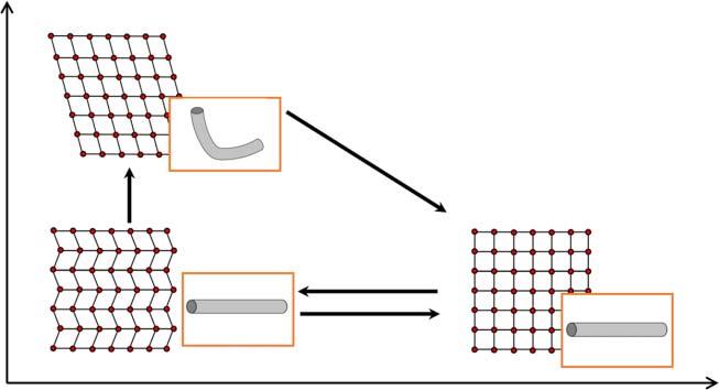
Shapememoryalloys(SMAs)arethemosttypicalferroelasticmaterial,which isanimportantmemberofferroics.Theshapememorycharacteristicsoriginatesfromthephasetransitionbetweenhightemperatureaustenitephaseand lowtemperaturemartensitephase,wheretheshapeatcubic-austenitephasecan beresumedfromlowtemperaturemartensitephasewhoselatticecanbelargely twisted(seeFigure1.13).
TheSMAshavebeenwidelyusedindevicesfrombraceoforthodontia andothermedicalapplications,airjet,satelliteantenna,etc.Researchwas carriedoutindevelopingsystemsthatwouldoptimizethechevron“immersion”
1.4FerroelasticMaterialandDeviceApplication
Figure1.12 OutlineofMEdevicefromVirginiaTechandschematicofthecross-sectionofthe MEcomposite.Source:Wangetal.(2011).AdaptedwithpermissionofJohnWileyandSons.
Figure1.13 Phasetransitionbetweenhightemperatureaustenitephaseandlow temperaturemartensitephase,wheretheshapeatcubic-austenitephasecanberesumed fromlowtemperaturemartensitephasewhoselatticecanbelargelytwisted.
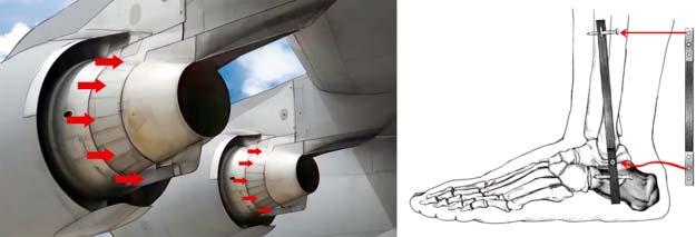
intothejetflowbasedontheflightcondition.AsshowninFigure1.14a, SMAsactivatedbyheatweredevelopedthatwouldallowforfullchevron immersioninjetflowduringhighthrustrequirements(e.g.duringtake-off) andnotimmersingitduringcruisewherethethrustefficiencyisofgreater importance(Anonn.d.).
Piezofiber
Figure1.14 (a)Braceoforthodontiausingshapememoryalloysand(b)arthrodesisdevice developedbyKarnesetal.
Forbrokenbonerehabilitation,aSMAplatewithamemorytransfertemperatureclosetobodytemperaturecanbeattachedtobothendsofthebrokenboneas showninFigure1.14b.Frombodyheat,theplatewillcontractandretainitsoriginalshape,thereforeexertingacompressionforceonthebrokenboneattheplace offracture.Afterthebonehashealed,theplatecontinuesexertingthecompressiveforceandaidsinstrengtheningduringrehabilitation(Garlocketal.2017).
1.5ScopeofThisBook
InChapters2–5,fundamentalsofferroelectrics,applicationsofferroelectric materials,recentadvances,andadvancedmeasurementandtestingtechniques inferroelectricswillbeintroduced.Inparticular,deviceapplicationsofferroelectricmaterialsinthinfilmformwillbeintroducedincludingFeRAM, ferroelectrictunneling-basedresistiveswitching,etc.Therecentadvances includeferroelectricityinemergingmaterialssuchas2Dmaterialsandhigh-k gatedielectricmaterialHfO2 ,whiletheadvancedcharacterizationtechnologies includethepiezoresponseforcemicroscopy(byimagingandswitchingferroelectricdomains)andCs-correctedtransmissionelectronmicroscopy(TEM) whereatomiclevelionicdisplacementcanbeidentified.
Asthemostimportantpropertyapplicationofferroelectricmaterials, fundamentalsofpiezoelectricphysicsandengineeringconsiderationsfordevice designandfabricationareintroducedinChapters6and7.
InChapter8,startingwithabriefintroductiononoriginofferromagnetismand itsanalogytoferroelectrics,deviceapplications,particularlyformagnetostrictive devices,areintroduced.
Chapters9and10willintroducethemultiferroicsofmaterialspossessingboth ferromagneticandferroelectricordersincludingsinglephaseandcomposite materials.Inparticular,devicesbasedontheintegrationofferroelectricand ferromagneticmaterialssuchasmultiferroicmemorydeviceandMEcoupling deviceforsensorapplicationswillbeintroduced.
InChapter11,ferroelasticmaterialsrepresentedbySMAandmagneticSMAs aswellastheirdeviceapplicationswillbeintroduced.
References
Boyn,S.,Grollier,J.,Lecerf,G.etal.(2017).Learningthroughferroelectricdomain dynamicsinsolid-statesynapses. NatureCommunications 8:1–7. Chang,C.-Y.andChen,T.-L.(2017).Design,fabrication,andmodelingofanovel dual-axiscontrolinputPZTgyroscope. Sensors 17(11):2505.
Cho,J.(2018). Amidcontradictoryforecast:ICinsights:‘Memorychipswillgrowat annualrateof5%onlyonaverageby2022’ .Seoul,Korea:BusinessKorea. Garlock,A.,Karnes,W.M.,Fonte,M.etal.(2017).Arthrodesisdevicesfor generatingandapplyingcompressionwithinjoints.US2017/0296241A1, Availableat:https://patents.google.com/patent/US20170296241A1/en. Li,M.,Dong,C.,Zhou,H.etal.(2017).HighlysensitiveDCmagneticfieldsensor basedonnonlinearMEeffect. IEEESensorsLetters 1(6):1–4.
RenesasElectronicsCorporation(2017).Renesaselectronicsachieveslarge-scale memoryoperationinfin-shapedMONOSflashmemoryforindustry’sfirst high-performance,highlyreliableMCUsin16/14nmprocessnodesandbeyond. Wang,Y.,Gray,D.,Berry,D.etal.(2011).Anextremelylowequivalentmagnetic noisemagnetoelectricsensor. AdvancedMaterials 23(35):4111–4114.Available at:https://doi.org/10.1002/adma.201100773.