

https://ebookmass.com/product/electronic-packaging-science-
Instant digital products (PDF, ePub, MOBI) ready for you
Download now and discover formats that fit your needs...
Sustainable Food Packaging Technology Athanassia Athanassiou
https://ebookmass.com/product/sustainable-food-packaging-technologyathanassia-athanassiou/
ebookmass.com
Biopolymer-Based Food Packaging: Innovations and Technology Santosh Kumar
https://ebookmass.com/product/biopolymer-based-food-packaginginnovations-and-technology-santosh-kumar/
ebookmass.com
Electronic materials : principles and applied science Poplavko
https://ebookmass.com/product/electronic-materials-principles-andapplied-science-poplavko/
ebookmass.com
Three
Streams: Confucian
Reflections
on Learning and the Moral Heart-Mind in China, Korea, and Japan Philip J Ivanhoe
https://ebookmass.com/product/three-streams-confucian-reflections-onlearning-and-the-moral-heart-mind-in-china-korea-and-japan-philip-jivanhoe/
ebookmass.com


Encyclopedia of Endocrine Diseases 2nd Edition Ilpo Huhtaniemi
https://ebookmass.com/product/encyclopedia-of-endocrine-diseases-2ndedition-ilpo-huhtaniemi/
ebookmass.com
The Engineer's Wife Tracey Enerson Wood
https://ebookmass.com/product/the-engineers-wife-tracey-enerson-wood/
ebookmass.com
The Economics of Banking and Finance in Africa: Developments in Africa’s Financial Systems Joshua Yindenaba Abor & Charles Komla Delali Adjasi
https://ebookmass.com/product/the-economics-of-banking-and-finance-inafrica-developments-in-africas-financial-systems-joshua-yindenabaabor-charles-komla-delali-adjasi/ ebookmass.com
The Forms of Michael Field Palgrave
https://ebookmass.com/product/the-forms-of-michael-field-palgrave/
ebookmass.com
A Study Guide for Danez Smith's "Tonight, in Oakland" Gale


https://ebookmass.com/product/a-study-guide-for-danez-smiths-tonightin-oakland-gale/
ebookmass.com

https://ebookmass.com/product/stand-by-me-pat-simmons/
ebookmass.com

Electronic Packaging Science and Technology
Electronic Packaging Science and Technology
King-Ning Tu
National Chiao Tung University, Hsinchu, Taiwan, ROC
Chih Chen
Department of Materials Science and Engineering, National Yang Ming Chiao Tung University, Hsinchu, Taiwan, ROC
Hung-Ming Chen
Institute of Electronics, National Yang Ming Chiao Tung University, Hsinchu, Taiwan, ROC
This edition first published 2022 © 2022 John Wiley & Sons, Inc.
All rights reserved. No part of this publication may be reproduced, stored in a retrieval system, or transmitted, in any form or by any means, electronic, mechanical, photocopying, recording or otherwise, except as permitted by law. Advice on how to obtain permission to reuse material from this title is available at http://www.wiley.com/go/permissions.
The right of King-Ning Tu, Chih Chen and Hung-Ming Chen to be identified as the authors of this work has been asserted in accordance with law.
Registered Office
John Wiley & Sons, Inc., 111 River Street, Hoboken, NJ 07030, USA
Editorial Office
111 River Street, Hoboken, NJ 07030, USA
For details of our global editorial offices, customer services, and more information about Wiley products visit us at www.wiley.com.
Wiley also publishes its books in a variety of electronic formats and by print-on-demand. Some content that appears in standard print versions of this book may not be available in other formats.
Limit of Liability/Disclaimer of Warranty
In view of ongoing research, equipment modifications, changes in governmental regulations, and the constant flow of information relating to the use of experimental reagents, equipment, and devices, the reader is urged to review and evaluate the information provided in the package insert or instructions for each chemical, piece of equipment, reagent, or device for, among other things, any changes in the instructions or indication of usage and for added warnings and precautions. While the publisher and authors have used their best efforts in preparing this work, they make no representations or warranties with respect to the accuracy or completeness of the contents of this work and specifically disclaim all warranties, including without limitation any implied warranties of merchantability or fitness for a particular purpose. No warranty may be created or extended by sales representatives, written sales materials or promotional statements for this work. The fact that an organization, website, or product is referred to in this work as a citation and/or potential source of further information does not mean that the publisher and authors endorse the information or services the organization, website, or product may provide or recommendations it may make. This work is sold with the understanding that the publisher is not engaged in rendering professional services. The advice and strategies contained herein may not be suitable for your situation. You should consult with a specialist where appropriate. Further, readers should be aware that websites listed in this work may have changed or disappeared between when this work was written and when it is read. Neither the publisher nor authors shall be liable for any loss of profit or any other commercial damages, including but not limited to special, incidental, consequential, or other damages.
Library of Congress
Cataloging-in-Publication Data
Names: Tu, K. N. (King-Ning), 1937– author. | Chen, Chih, 1970– author. | Chen, Hung-Ming, author.
Title: Electronic packaging science and technology / King-Ning Tu, University of California, Los Angeles, United States of America; Chih Chen, National Chiao Tung University, Hsinchu, Taiwain; Hung-Ming Chen, National Chiao Tung University, Hsinchu, Taiwain.
Description: 1st edition. | Hoboken, NJ : Wiley, 2022. | Includes bibliographical references and index.
Identifiers: LCCN 2021039114 (print) | LCCN 2021039115 (ebook) | ISBN 9781119418313 (cloth) | ISBN 9781119418320 (adobe pdf) | ISBN 9781119418337 (epub)
Classification: LCC TK7870.15 .T8 2022 (print) | LCC TK7870.15 (ebook) | DDC 621.381/046–dc23
LC record available at https://lccn.loc.gov/2021039114
LC ebook record available at https://lccn.loc.gov/2021039115
Cover image: © Andriy Onufriyenko/Getty Images
Cover design by Wiley
Set in 9.5/12.5pt STIXTwoText by Strive, Pondicherry, India
10 9 8 7 6 5 4 3 2 1
Contents
Preface xi
1 Introduction 1
1.1 Introduction 1
1.2 Impact of Moore’s Law on Si Technology 3
1.3 5G Technology and AI Applications 4
1.4 3D IC Packaging Technology 7
1.5 Reliability Science and Engineering 11
1.6 The Future of Electronic Packaging Technology 13
1.7 Outline of the Book 14
References 15
Part I 17
2 Cu-to-Cu and Other Bonding Technologies in Electronic Packaging 19
2.1 Introduction 19
2.2 Wire Bonding 20
2.3 Tape-Automated Bonding 23
2.4 Flip- Chip Solder Joint Bonding 26
2.5 Micro-Bump Bonding 32
2.6 Cu-to- Cu Direct Bonding 35
2.6.1 Critical Factors for Cu-to- Cu Bonding 36
2.6.2 Analysis of Cu-to- Cu Bonding Mechanism 39
2.6.3 Microstructures at the Cu-to- Cu Bonding Interface 46
2.7 Hybrid Bonding 51
2.8 Reliability – Electromigration and Temperature Cycling Tests 54 Problems 56
References 57
3 Randomly-Oriented and (111) Uni-directionally-Oriented Nanotwin Copper 61
3.1 Introduction 61
3.2 Formation Mechanism of Nanotwin Cu 63
3.3 In Situ Measurement of Stress Evolution During Nanotwin Deposition 67
3.4 Electrodeposition of Randomly Oriented Nanotwinned Copper 69
3.5 Formation of Unidirectionally (111)-oriented Nanotwin Copper 71
3.6 Grain Growth in [111]- Oriented nt- Cu 75
3.7 Uni-directional Growth of η- Cu6Sn5 in Microbumps on (111) Oriented nt- Cu 77
3.8 Low Thermal-Budget Cu-to- Cu Bonding Using [111]- Oriented nt- Cu 78
3.9 Nanotwin Cu RDL for Fanout Package and 3D IC Integration 83
Problems 86
References 87
4 Solid–Liquid Interfacial Diffusion Reaction (SLID) Between Copper and Solder 91
4.1 Introduction 91
4.2 Kinetics of Scallop-Type IMC Growth in SLID 93
4.3 A Simple Model for the Growth of Mono-Size Hemispheres 95
4.4 Theory of Flux-Driven Ripening 97
4.5 Measurement of the Nano-channel Width Between Two Scallops 100
4.6 Extremely Rapid Grain Growth in Scallop-Type Cu6Sn5 in SLID 100
Problems 102
References 103
5 Solid-State Reactions Between Copper and Solder 105
5.1 Introduction 105
5.2 Layer-Type Growth of IMC in Solid-State Reactions 106
5.3 Wagner Diffusivity 111
5.4 Kirkendall Void Formation in Cu3Sn 113
5.5 Sidewall Reaction to Form Porous Cu3Sn in μ-Bumps 114
5.6 Effect of Surface Diffusion on IMC Formation in Pillar-Type μ-Bumps 120
Problems 124 References 125
Part II 127
6 Essence of Integrated Circuits and Packaging Design 129
6.1 Introduction 129
6.2 Transistor and Interconnect Scaling 131
6.3 Circuit Design and LSI 133
6.4 System-on- Chip (SoC) and Multicore Architectures 139
6.5 System-in-Package (SiP) and Package Technology Evolution 140
6.6 3D IC Integration and 3D Silicon Integration 144
6.7 Heterogeneous Integration: An Introduction 145 Problems 146 References 146
7 Performance, Power, Thermal, and Reliability 149
7.1 Introduction 149
7.2 Field-Effect Transistor and Memory Basics 151
7.3 Performance: A Race in Early IC Design 155
7.4 Trend in Low Power 157
7.5 Trade-off between Performance and Power 159
7.6 Power Delivery and Clock Distribution Networks 160
7.7 Low-Power Design Architectures 163
7.8 Thermal Problems in IC and Package 166
7.9 Signal Integrity and Power Integrity (SI/PI) 168
7.10 Robustness: Reliability and Variability 169 Problems 171 References 172
8 2.5D/3D System-in-Packaging Integration 173
8.1 Introduction 173
8.2 2.5D IC: Redistribution Layer (RDL) and TSV-Interposer 174
8.3 2.5D IC: Silicon, Glass, and Organic Substrates 176
8.4 2.5D IC: HBM on Silicon Interposer 177
8.5 3D IC: Memory Bandwidth Challenge for High-Performance Computing 178
8.6 3D IC: Electrical and Thermal TSVs 180
8.7 3D IC: 3D-Stacked Memory and Integrated Memory Controller 182
8.8 Innovative Packaging for Modern Chips/Chiplets 183
8.9 Power Distribution for 3D IC Integration 186
8.10 Challenge and Trend 187 Problems 188 References 188
Part III 191
9 Irreversible Processes in Electronic Packaging Technology 193
9.1 Introduction 193
9.2 Flow in Open Systems 196
9.3 Entropy Production 198
9.3.1 Electrical Conduction 199
9.3.1.1 Joule Heating 201
9.3.2 Atomic Diffusion 203
9.3.3 Heat Conduction 203
9.3.4 Conjugate Forces When Temperature Is a Variable 205
9.4 Cross-Effects in Irreversible Processes 206
9.5 Cross-Effect Between Atomic Diffusion and Electrical Conduction 207
9.5.1 Electromigration and Stress-Migration in Al Strips 209
9.6 Irreversible Processes in Thermomigration 211
9.6.1 Thermomigration in Unpowered Composite Solder Joints 212
9.7 Cross-Effect Between Heat Conduction and Electrical Conduction 215
9.7.1 Seebeck Effect 216
9.7.2 Peltier Effect 218
Problems 219 References 219
10 Electromigration 221
10.1 Introduction 221
10.2 To Compare the Parameters in Atomic Diffusion and Electric Conduction 222
10.3 Basic of Electromigration 224
10.3.1 Electron Wind Force 225
10.3.2 Calculation of the Effective Charge Number 227
10.3.3 Atomic Flux Divergence Induced Electromigration Damage 228
10.3.4 Back Stress in Electromigration 230
10.4 Current Crowding and Electromigration in 3-Dimensional Circuits 231
10.4.1 Void Formation in the Low Current Density Region 234
10.4.2 Current Density Gradient Force in Electromigration 238
10.4.3 Current Crowding Induced Pancake-Type Void Formation in Flip- Chip Solder Joints 242
10.5 Joule Heating and Heat Dissipation 243
10.5.1 Joule Heating and Electromigration 244
10.5.2 Joule Heating on Mean-Time-to-Failure in Electromigration 245 Problems 245
References 246
11
Thermomigration 249
11.1 Introduction 249
11.2 Driving Force of Thermomigration 249
11.3 Analysis of Heat of Transport, Q* 250
11.4 Thermomigration Due to Heat Transfer Between Neighboring Pairs of Powered and Unpowered Solder Joints 253 Problems 255
References 255
12
Stress-Migration 257
12.1 Introduction 257
12.2 Chemical Potential in a Stressed Solid 258
12.3 Stoney’s Equation of Biaxial Stress in Thin Films 260
12.4 Diffusional Creep 264
12.5 Spontaneous Sn Whisker Growth at Room Temperature 267
12.5.1 Morphology 267
12.5.2 Measurement of the Driving Force to Grow a Sn Whisker 271
12.5.3 Kinetics of Sn Whisker Growth 272
12.5.4 Electromigration-Induced Sn Whisker Growth in Solder Joints 275
12.6 Comparison of Driving Forces Among Electromigration, Thermomigration, and Stress-Migration 277
12.6.1 Products of Force 278
Problems 279
References 280
13 Failure Analysis 281
13.1 Introduction 281
13.2 Microstructure Change with or Without Lattice Shift 285
13.3 Statistical Analysis of Failure 287
Contents x
13.3.1 Black’s Equation of MTTF for Electromigration 287
13.3.2 Weibull Distribution Function and JMA Theory of Phase Transformations 289
13.4 A Unified Model of MTTF for Electromigration, Thermomigration, and Stress-Migration 290
13.4.1 Revisit Black’s Equation of MTTF for Electromigration 290
13.4.2 MTTF for Thermomigration 292
13.4.3 MTTF for Stress-Migration 292
13.4.4 The Link Among MTTF for Electromigration, Thermomigration, and Stress-Migration 293
13.4.5 MTTF Equations for Other Irreversible Processes in Open Systems 293
13.5 Failure Analysis in Mobile Technology 293
13.5.1 Joule Heating Enhanced Electromigration Failure of Weak-Link in 2.5D IC Technology 294
13.5.2 Joule Heating Induced Thermomigration Failure Due to Thermal Crosstalk in 2.5D IC Technology 298 Problems 301 References 302
14 Artificial Intelligence in Electronic Packaging Reliability 303
14.1 Introduction 303
14.2 To Change Time-Dependent Event to Time-Independent Event 304
14.3 To Deduce MTTF from Mean Microstructure Change to Failure 305
14.4 Summary 306 Index 307
Preface
As we enter the big data era, mobile devices are ubiquitous. Internet of things (IoT) is everywhere, and we have man-to-man, man-to-machine, and machine-to-machine communications. Furthermore, in the Covid-19 virus pandemic period, the trend of distance teaching, distance medicine, home office, and on-line meeting has increased greatly the need of advanced consumer electronic products, demanding smaller form factor, larger memory, more functions, faster and larger data collection and transmission, cheaper cost, and superb reliability. At the same time, 5G advanced communication technology and 3D IC devices have begun their impact to our society, and many new artificial intelligence (AI) applications have been invented.
With the perceived slowing down of Moore’s law of miniaturization of Si chip technology, microelectronic industry is searching for alternative ways to sustain Moore’s law. 3D IC is most promising in achieving more-thanMoore, wherein the up-scale of packaging technology is critical. Indeed, new advanced packaging factories are being built worldwide. We ask what will be the technical innovations in electronic packaging for 3D IC devices in order to enhance performance and reliability? Or, what are the challenging issues in electronic packaging technology that are essential in the near future development of semiconductor technology?
The goal of this book to present the science and engineering of advanced electronic packaging technology for a deeper understanding of the essence in development and manufacturing of the more-than-Moore technology. Especially, what is new in this book are the subjects of Cu-to- Cu direct bonding by using the (111) uni-directionally oriented nanotwin Cu, innovative 3D IC systems in packaging integration for high performance of wide bandwidth and low power devices, and the analysis of mean-time-to-failure equations based on entropy production.
After the introduction chapter, the following chapters will be divided into three parts. In Part I, the history of bonding technology will be covered in
Chapter 2, starting from wire-bonding, tab-automated bonding, flip chip C-4 solder joint bonding, micro-bump bonding, Cu-to- Cu direct bonding, and hybrid bonding. The microstructure, properties, and applications of randomly oriented and (111) uni-directionally oriented nano-twin Cu will be covered in Chapter 3. Then, Chapter 4 and Chapter 5 will be dedicated to chemical reactions and kinetic processes in Cu-Sn reactions for solder joint formation. Chapter 4 will review solid-liquid interfacial diffusion (SLID) reactions between liquid solder and Cu. Chapter 5 will review solid-solid reactions between solid solder and Cu. The kinetics of growth of intermetallic compound (IMC), which is a stoichiometric compound and has no composition gradient, has been an outstanding problem in solid-solid reactions. We introduce Wagner’s diffusivity to overcome it.
Part II consists of chapters on electric circuit integration in packaging technology. The emphasis is on the design of low power devices and intelligent integration. The technical issues related to the need for faster rates and increased amounts of data transport in 2.5D/3D IC are discussed. It is explained how to increase the I/O density and the bandwidth in packaging technology.
Part III is a collection of chapters on reliability science. It begins with a chapter on irreversible processes of atomic flow, heat flow, and charge flow in open systems. The most important issue of Joule heating will be analyzed. The topics of electromigration, thermomigration, stress migration, and failure analysis will be covered. Equations of mean-time-to-failure (MTTF) will be reanalyzed on the basis of entropy production.
Finally, in Chapter 14, a brief discussion on how to use artificial intelligence to accelerate reliability testing will be presented. We propose an x-ray based graphic processing unit (X- GPU) to analyze early reliability failure before it occurs in any newly developed 3D IC device for mass production. The goal of AI here is to change the time-dependent and time-consuming reliability tests to time- independent tests. The basic idea of mean microstructure-change to failure (MMTF) will be introduced, so that we can link MTTF to MMTF.
We appreciate the capable help of Mrs. Jody Lee and Mr. John Wu at NCTU in preparing the book.
Hsinchu, December 2020 King-Ning Tu Chih Chen Hung-Ming Chen
Introduction
1.1 Introduction
As we enter the big data era, mobile devices are ubiquitous. On hardware, nearly everyone has a cell phone. On software, internet of things (IOT) reaches everywhere. We have man-to-man, man-to-machine, and machineto-machine communications. Furthermore, during the Covid-19 virus pandemic, the trend of distance teaching, distance medicine, home office, and online meeting has increased greatly the need of advanced consumer electronic products, demanding smaller form factor, larger memory, more function, cheaper cost, faster and greater rate of data transmission, and superb reliability. Actually, the advanced 5G communication technology and 3-dimensional integration of circuits (3D IC) have already begun their impact to our society. No doubt the world around us is changing rapidly. In human history, this is the second time of a fundamental revolution.
In eighteenth century, we had industrial revolution when steam engine was invented. It developed machine power to replace human power and animal power. The activities in civilization were changing from agriculture to industry. We had railroad trains, ocean liners, automobiles, airplanes, and electricity. While industrial production has transformed human society from feudal to democratic, it was accompanied by capitalism, then communism, and then socialism. Indeed, the impact to human society was huge in the last two to three hundred years.
In twentieth century, after the invention of transistor, very-large-scale integration of transistor circuits, and mobile technology, we have data power to enhance machine power. What is coming is to have artificial intelligence (AI) revolution. We have robots, and human-less vehicles and
Electronic Packaging Science and Technology, First Edition. King-Ning Tu, Chih Chen, and Hung-Ming Chen.
© 2022 John Wiley & Sons, Inc. Published 2022 by John Wiley & Sons, Inc.
aircrafts to serve us. Mobile technology supported by mobile internet will have a long way to go in the near future. Accompanying the rapid progress, however, Moore’s law of miniaturization in Si chip technology is near ending, so people wonder whether the rapid progress can be sustained.
If we look back to the last 10–20 years, semiconductor industry has had some interesting events. Namely, Japan has lost the leadership in semiconductor technology. The large European countries such as England, France, and Russia have no presence in microelectronics. On the other hand, Taiwan and Korea have gained the leadership due to the success of Taiwan Semiconductor Manufacturing Corporation (TSMC) and Samsung. Today, China has identified semiconductor device development and manufacturing to be a national goal and will spend a large sum of money to achieve it. One of the key reasons behind the trade war between United States and China is due to the competition in advanced semiconductor technology and in manufacturing of consumer electronic products. At the same time, 5G communication technology and AI applications are with us and they exert an unlimited impact and change to our society.
There were many reasons of Japan’s failure, such as the critical change in currency exchange rate between yuan and dollar, and also the heavy punishments of Fujitsu by United States. However, Japan has recently joined TSMC to form an advanced electronic packaging factory in Japan to maintain its impact. The weaker and weaker presence of England and France is because of the insufficient financial support on semiconductor technology due to socialism. They tended to support rather uniformly the popular needs of society, but did not concentrate on supporting semiconductor technology. Today, to build a Si-based transistor factory will take 3–5 billion US dollars, so fewer and fewer countries can afford it. Russia is simply poor. Samsung in Korea has had the government’s focused support to do so. TSMC in Taiwan is unique that it takes orders from all over the world to make VLSI devices, so it knows the major trend of the technology. Thus, it can spend the money it earned to keep improving the technology with innovation. For example, the technique of immersion lithography has enabled TSMC to lead the manufacturing of nanoscale semiconductor devices for the past five generations. Now, we are having the 5 nm node of nanotechnology, and 3 nm and 2 nm nodes are coming.
Some experts in China commented that China might take 10 years to catch up. No reason was given why it will take so long! On the other hand, China has been very successful in high-speed train and satellite technology. When China can make transistors as cheap as those made in United States, it is a sign that China has caught up. A plausible reason is given below.
1.2 IImpctoof oorre’s paw on i rccnoooog 3
A Chinese classic philosopher, Wang Yang-Ming, said “Knowing is hard, but practice is easy.” Semiconductor technology is completely opposite that “Knowing is easy, but practice is hard.” Take an example of teaching a child to play violin or piano; we can find the best teacher to teach the child all the technique and tricks of how to play well. Even a very talented child, he/she still has to take 10–20 years of practice to be good. It is the “experience” that is needed to do well. Indeed, “experience” cannot be taught quickly and cannot be copied or cannot be steal. Furthermore, in semiconductor manufacturing, the experience is not just of one person, it is of an entire industry.
1.2 Impact of Moore’s Law on Si Technology
Moore’s law states that the transistor density per chip area is doubling every 18–24 months without the increase of production cost. Figure 1.1 depicts the achievements of 2D IC of Si technology according to Moore’s law. From 1970 to 1985, the density has increased from 1K to 1M per chip, which is an increase of 1000 times. From 1985 to 2005, the increase was from 1M to 1G, which is another increase of 1000 times. It is the most successful event of sustainability for about 40 years of any human activity.
Figure 1.1 A sketch of the achievements of 2D IC of Si technology according to Moore’s law.
There are 110 Si chips in the module of a mainframe Computer in 2002.
IBM J. of R&D., November, 2002.
If we replace the 110 chips by 1 chip, we can make the mobile phone now!
Also replace key-board by nger-touch.
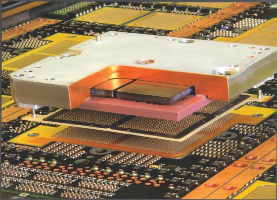
Figure 1.2 An image of part of the device structure of the mainframe computer in 2002. The size of the module is about 10 × 10 cm.
The law has had two significant impacts. First, the price of one transistor is now cheaper than the printing of one alphabet on a newspaper, which is a significant consequence of the Moore’s law that circuit density can be doubled without the increase of production cost. Hence, we can have very low cost use of transistors. Second, it enables the reduction of physical size of a computer so that handheld and mobile devices can be made. Figure 1.2 shows part of a mainframe computer in 2002. The module size is about 10 × 10 cm, and between two of the ceramic plates in the module, there are 10 × 11 = 110 pieces of Si chips. According to Moore’s law shown in Figure 1.1, the circuit density per chip in 2002 is about 256 M. If we can integrate the central processing unit (CPU) and the memory on the 110 chips into a single chip, we can build a mobile device or a mobile computer by using a single chip! No doubt, we also need to reduce the packaging structure, as well as to replace a keyboard by the finger-touching technique. It is worth mentioning that in Figure 1.2, while we do not see the chips but we see the electronic packaging structure, wherein the bright solder joints are everywhere. It shows how important is solder joint technology in electronic device manufacturing. This is because solder joint is still the best way to join two Cu wires, even two nanowires of Cu.
1.3 5G Technology and AI Applications
Those advances mentioned in the above have changed internet to mobile internet. Internet means computer-to-computer communication. Mobile internet means mobile computer (cell phone)-to-mobile computer communication. At this moment, the rapid advances in 5G and AI require Moore’s
1.3 5G rccnoooogpnd I mmoicption’s 5
law to keep going ahead for at the least another 10–20 years, but Moore’s law is ending.
In human civilization, the technique of communication has advanced step-by-step slowly from language, written words, printing, telephone and telegraph, television, internet, and now to mobile internet. Today, the advanced communication technology behind mobile internet is defined as 5G, with a standard of certain required performance. Figure 1.3 shows the drawing of a flower, which has six petals. There are two sets of petals: the inner brighter ones and the outer darker ones. The latter represents 5G technology and the former represents 4G technology. Each petal defines a specific technical requirement, as shown in Table 1.1. For example, on
User experienced data rate (Gbps) 0.1 to 1 Gbps
Traf c volume density (Tbps/km2)
of Tbps/km2
Figure 1.3 The petals of flower, which shows the required functions in 4G and 5G communication technology.
Table 1.1 5G technical requirements.
● Primary requirements:
End-to-end latency (mille sec)
Peak data rate (mobility, km/h)
Traffic volume density (tens of Tbps/km2)
Density of base stations (104/km2)
Internet of everything
Energy efficiency
● Secondary requirements:
Security and reliability
Low cost
point-to-point latency of signals, it was 10 ms in 4G and about 1 ms in 5G. If we can advance the required performance beyond the petals of 5G, it will be 6G.
In 2014, it was already predicted that around 2020, the 5G technology will be widely available. However, the company, Huawei in China, announced that its 5G technology is ready in 2019, ahead of everyone. It became a critical issue in the trade war between China and United States. The latter has put Huawei on its entity list or ban list. The hardware in 5G consists of satellites, servers, optical fiber lines, base stations, cell phones, and terminal sensors, and the software consists of various mobile internets, such as Android of Google. Huawei is especially good at making base stations.
Data and signals can be transmitted via satellites in sky, but satellites can be shot down easily in the beginning of a war. It can be transmitted via optical fibers underground and across oceans. The making of optical fiber requires the doping of rare-earth elements, so the strategic importance of rare-earth elements can be appreciated. Also it can be transmitted via base stations on land surface, so the construction of a large number of base stations is of national security concern. It is worth mentioning that Taiwan has successfully used its network of base stations to detect and control the motion and contact of people with Covid virus.
In the late nineties, dot-com was developed but soon burst because cell phones were not available. After cell phone becomes popular, Apple, Microsoft, Amazon, etc. are now the biggest companies in the world, no more GE, IBM, and Exxon, because of the wide applications of mobile technology.
About the global standard of requirements in 5G technology, see Table 1.1, the first is point-to-point latency of signals, which is only a few milli second. Latency means the total time spent to send out a signal and to receive it back. In a chain of moving cars, if the first car stops suddenly, the second car must stop within the time of latency, otherwise an accident would occur. If we consider a human-less vehicle, the LiDAR (not radar) on top of the car should be able to detect a sudden appearance of a pedestrian or a car, so that it can stop to avoid an accident.
Moreover, LiDAR and radar are line- of- sight techniques. Yet, we need to have a network of vehicle-to- everything in order to have non-line- ofsight awareness to know what is behind a stationary or a moving object. Also it should have an ultrafast rate of transport of data in order to show clearly the change of images of the surrounding of a car moving at high speed. Besides, it can download or upload instantly news or weather reports. To download a movie will now take only three seconds in 5G technology. For the success of 5G, it must have a very large number of base stations, so that information can be received and transmitted
continuously from place to place. It is no need to explain other standard requirements in Table 1.1, they should be clear. For example, any device being used under the hood of a car should have a high reliability because of heat. Then, low cost is important for the use of internet of everything in our home and office.
No doubt, 5G technology will enhance AI applications. At the end of this book, in Chapter 14, we shall discuss the need of using AI to accelerate the study of reliability, so that we may change it from a time-dependent event to a time-independent event. Another area for the use of AI will be the biomedical and health applications. For example, Chinese medicine has been based on big data for many years, and the technique of acupuncture could be improved with modern microelectronic devices. The link between microelectronics and biomedical applications will be the most important advanced technology in the future.
1.4 3D IC Packaging Technology
As the trend of miniaturization in Si technology slows down, microelectronics industry has been looking for ways to keep the downsizing momentum going, meaning to go to more-than-Moore! [1–3] The critical feature size in Si devices has already reached nanoscale, below 10 nm. Hence, it is harder and harder to make transistor circuits on a Si chip smaller and smaller without a large cost increase. At present, the most promising way to extend Moore’s law is to go from 2D IC to 3D IC. Actually, the paradigm change has occurred more than 10 years ago, but 3D IC is not in mass production, because of cost and reliability.
In semiconductor manufacturing, because the product quantity is extremely large, so high yield and high reliability are critically important. Low yield will increase cost, and poor reliability will lead to recall; one example is the battery failure of cell phones. For any consumer electronic product in mass production, the concern of reliability is critical, especially the electronic packaging in 3D IC for advanced consumer electronic products, which are widely used now for distance teaching and home office.
In this introductory chapter, we explain what is electronic packaging? Also, what are the science and engineering in it, especially those relate to reliability? If we want to add more functions to hand-held devices, the operations of memory, logic, and special functions must be increased. At the same time, power as well as battery capacity must be increased too. A larger size battery will squeeze the volume of the rest of the device, which makes the heating problem worse. To remove heat, we must have a
temperature gradient. If we consider a temperature difference of 1 °C across a microstructure of 10 μm in diameter, the temperature gradient is 1000 °C/cm, which will induce thermomigration. In turn, Joule heating will enhance electromigration, and thermo-stress will induce stressmigration. While these are time-dependent events, they are of major reliability concern.
Figure 1.4 is a scanning electron microscopy (SEM) image of the crosssection of a 2.5D IC test device. It has only two pieces of Si chips stacking on a polymer board. Electrically, they are interconnected by three sets of solder joints. At the bottom or on the outside of the polymer board is the set of the largest solder balls of diameter up to 760 μm, which is called the ball-gridarray (BGA). These balls allow the test device to be connected to the circuits on a printed circuit board. Within the polymer board, there are Cu wirings, as well as Cu plated-through-holes, which are not shown in the image. On top of the polymer board, there is the second set of flip chip solder balls of diameter about 100 μm, the so-called C-4 (controlled collapse chip connection) solder balls, connecting the board to the first Si chip, which is the “interposer.” In this test device, there is no transistor on the interposer, which is passive and serves only as a substrate without introducing thermal stress to the active Si chip on the top. Often this test device is called 2.5D IC due to the fact that the interposer has no transistors. If the interposer has transistors, it becomes 3D IC.
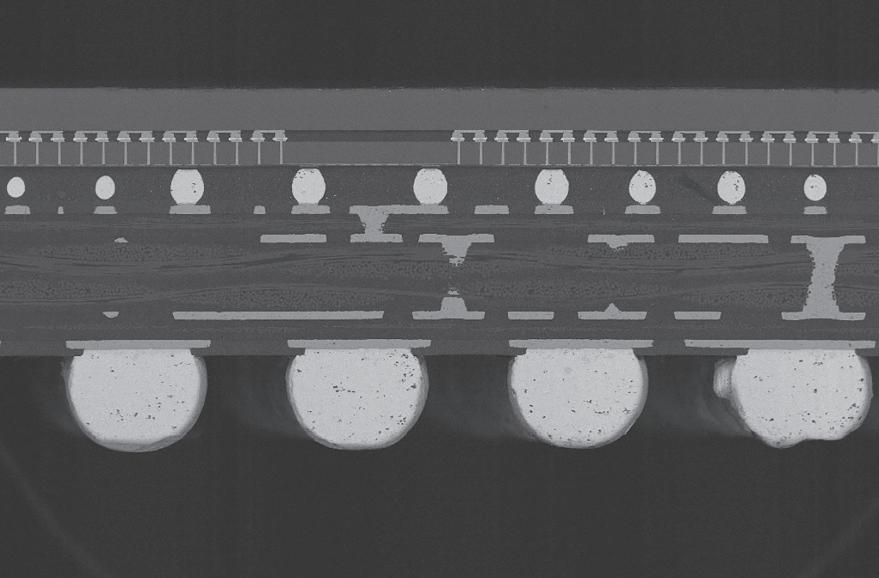
Figure 1.4 Scanning electron microscopy (SEM) image of the cross-section of a 3D IC test device. It has only two pieces of Si chips stacking on a polymer board.
In the interposer, there are arrays of vertical through-Si-vias (TSV) plated with Cu, making connections to the third arrays of solder joints of diameter about 10–20 μm, the so-called micro-bumps or μ-bumps, which join the interposer to the top Si chip. The top Si chip is an active device chip, so it has transistors. The thickness of the device in Figure 1.4 is about that of a US penny. The thinness of the device is a critical requirement due to the limit of form factor of mobile consumer electronic products. Consequently, the thickness of Si chips is thin too. The thickness of the Si interposer is about 50 μm, which is much thinner than that of a convention Si chip of 200 μm in thickness. The thin interposer has caused the warpage problem, as well as the heat conduction issue, to be discussed in the later chapters. The diameter of the TSV in the interposer is about 5 μm, so the aspect ratio of the TSV is 10.
In the above example, besides the active Si chip, the rest, which includes the interposer, can be regarded as electronic packaging. The packaging enables the Si chip to function, as well as to allow us, to interact with the outside world. In the packaging, it is worth mentioning that between two sets of solder joints of different sizes, there should be a redistribution layer (RDL) structure for circuit fan-out. It increases the number of input–output (I/O) contacts of a circuit in going from a low density of solder joints to a high density of solder joints. The higher the density of I/O, the better the resolution of frequency of a digital electromagnetic wave, because each I/O is designed to transmit a small width of the wave.
At the moment, there are two critically important challenges in electronic packaging technology. The first is the need of denser and denser I/O, which means the diameter of micro-bump and the pitch between them has to be reduced. As to be shown in Chapter 3, hybrid-bonds consist of Cu-to- Cu bonds together with dielectric-to-dielectric bonds are being developed. The second is Joule heating and heat dissipation, which will be discussed in Chapter 9.
About the increase of I/O, from BGA to C-4 joints, there is a RDL of Cu wires in the upper part of the polymer board. From C-4 joints to μ-bumps, there is an RDL of Cu wires at the lower part of the interposer chip. This second RDL is invisible in the figure, but it is new in 3D IC because it does not exist in 2D IC devices, where typically there are only two levels of solder joints. The failure of the new RDL is of concern.
Figure 1.5a and b show synchrotron radiation tomographic images of a 3D IC and part of a 2.5D IC device, respectively. The latter has a length about 4 mm, and a thickness and a height of about 0.5 mm. Due to the weak absorption of X-ray, the two Si chips and the polymer substrate become invisible. We can see the vertical TSV pillars. Also, the solder balls and the

Figure 1.5 (a) Synchrotron radiation tomographic images of a similar device as shown in Figure 1.1. Due to the weak absorption of X-ray, the two Si chips and the polymer substrate become invisible. But the solder balls and the Cu wires are shown clearly. (b) Synchrotron radiation tomographic image of a 2.5D IC device, having a length about 4 mm, and a thickness and a height of about 0.5 mm. The vertical TSV pillars can be seen.
Cu wires are shown clearly. In Figure 1.5a, by using a pair of the BGA balls as the cathode and the anode and by passing 50 mA at 100 °C, following the arrows which indicate the conduction path, we can study time-dependent failures caused by electromigration and Joule heating, to be discussed in Chapter 10.
Why do we emphasize electromigration and Joule heating? This is because electronic devices are current–voltage (I-V) devices, so the applied electric current goes in and out of the devices in an open system. It causes Joule heating and electromigration, which are of key reliability concern. Figure 1.6 is a schematic diagram of the cross- section of a typical 3D IC device. The structure, in essence, is the same as that shown in Figure 1.4, except that on the right-hand side, there is a stack of memory chips on a logic chip as the CPU. If we replace the stack by an optical or
1.5 Relialelity SlReSRiend enleRRelen
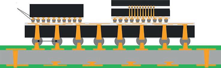
Schematic diagram of the cross-section of a typical 3D IC device.
compound semiconductor or MEMS chip, it becomes heterogeneous integration.
In comparing the structure of 3D IC to that of 2D IC, the difference is the stacking of multilayer of chips and the interconnects using TSV and μ-bumps. On processing TSV, the thinner the chip, the easier the drilling of vias. On making μ-bumps, its melting point should be lower than that of C-4 joints, so that the latter will not melt upon the melting of the former. Thus, the basic challenges are that the wafer is thinner and the processing temperature is lower.
From the viewpoint of packaging technology, we may say that the essence or the major challenge in 3D IC is to scale down the dimension of packaging structures so that it can match those in the chip technology. There is no Moore’s law in packaging technology, so it has room to shrink.
What are the key functions of electronic packaging? The cell phone held in our hands is a movable electronic packaging product or a mobile computer, which enables us to compute and to communicate with the world around us. The set of chips in the cell phone can be arranged horizontally, side by side, but it takes space. Or they can be arranged vertically, one on top of the other, this is called 3D IC, and it reduces the form factor and takes less space. However, heat dissipation in 3D IC is harder because the packing is denser. When over-heat occurs, it induces reliability problems. Over all, the product should be electrically, mechanically, chemically, and thermally stable.
1.5 Reliability Science and Engineering
An electronic device in operation is an open system because electrical charges flow in and out of the device. While the number of charges in transport is conserved, entropy production is not. The waste heat in entropy
production is Joule heating on the basis of irreversible processes. [4, 5] For electrical conduction, Onsager’s Eq. (1.1) below shows that entropy production is the product of the conjugated flux of j (current density = coulomb/cm2-sec) and the conjugated driving force of E (electric field E = jρ, where ρ is resistivity). Derivation of the Onsager equation will be given in Chapter 9.
where T is the temperature, V is the volume of sample, dS/dt is the entropy production rate, and j2 ρ is the Joule heating per unit volume per unit time. Typically, the power from Joule heating is written as P = I2R = j2 ρV, where I is the applied current and R is the resistance of the sample. Thus, j2 ρ is power density or Joule heating per unit volume per unit time of the sample, in units of Watt/cm3, and I2R is Joule heating per unit time for the entire sample, in units of Watt. Clearly, this is the reason why we need low-power devices or low entropy production devices.
While the cost of production of 3D IC can be reduced when it is in mass production, the problem of reliability due to over-heating has to be solved fundamentally by a smart system design or by design-for-reliability (DfR) and by a critical selection in materials integration. To put it simply, we need to design low-power devices, and also we need to understand heat production (Joule heating) in irreversible processes and heat dissipation in the device structure. [6] Hence, the science and engineering of electronic packaging come into focus.
Entropy production is the most relevant understanding of failure induced by electromigration, thermomigration, and stress-migration in irreversible processes. [7] Statistical analysis of failure requires the knowing of meantime-to-failure (MTTF). An example is Black’s equation of MTTF for elctromigration. In Chapter 13, we shall present a unified model of MTTF for electromigration, thermomigration, and stress-migration on the basis of entropy production.
Figure 1.7 shows an example of electromigration-induced damage in Cu interconnects. The high current density in the interconnect has induced a flow of atoms along the electron flow direction, going from the cathode to the anode, leading to vacancy accumulation and void formation in the cathode region. Resistance of the interconnect increases gradually until an opening in the circuit occurs, where the resistance increases dramatically.
Cu/dielectric cap interface
Current crowding
Current crowding
Cu/dielectric cap interface

Figure 1.7 An example of electromigration electromigration-induced failure of void formation in Cu interconnects. (a) Electrons drifted from the bottom Cu line to the top Cu line. (b) Electrons drifted from the top Cu line to the bottom Cu line.
1.6 The Future of Electronic Packaging Technology
In the near future, the R&D of packaging technology for 3D IC devices will be the focus. The role of electronic packaging in Si-based microelectronic technology is getting more and more important. In turn, reliability will be of major concern. The introduction of AI to facilitate the applications to new 3D IC devices and the reduction of the time-consuming reliability tests will demand our concentrated effort. In the long run, the applications of electronic packaging technology to biomedical devices will be important. For example, as people lives longer, diabetes is common in old age. To
determine oxygen content and sugar content in our blood, we use invasive method to obtain a drop of blood from our finger for measurement. It is very unpleasant! If we can invent a noninvasive method, for example by wearing a mobile device around our finger or arm, it will greatly reduce the unpleasant feeling in our daily live if we have diabetes. Even better, if we can implant a small device in our body to perform the blood testing function, we will need to understand the interfacial interaction between biological and nonbiological materials. In other words, we will need to study biocompactable materials, as well as the chemical reactions in body fluid at body temperature. Furthermore, we may need to join a biomaterial to a non-biomaterial. To do so, we may need a low-temperature solder or binder which can decompose slowly in the body. However, the melting point of the common Pb-free solder, the eutectic SnAg, is over 200 °C, to be discussed in Chapter 4 on solder joint reactions. We may need a new solder whose wetting temperature is around 100 °C, which is above the working temperature and near the body temperature, for biomedical devices. While these issues are beyond the scope of this book, we note that the future of electronic packaging technology has a long way to go.
1.7 Outline of the Book
The following chapters will be divided into three parts. In Part I, we cover briefly the history of bonding technology in Chapter 2, starting from wirebonding, tab-automated bonding (TAB), flip chip C-4 solder joint bonding, micro-bump bonding, Cu-to- Cu direct bonding, and hybrid bonding. In Chapter 3, we shall cover the structure, properties, and applications of randomly oriented and (111) unidirectionally oriented nano-twin Cu. Then, Chapters 4 and 5 will be dedicated to chemical reactions and kinetic processes in solder joint formation. Chapter 4 will review solid–liquid interfacial diffusion (SLID) reactions between liquid solder and Cu. Chapter 5 will review solid–solid reactions between solid solder and Cu upon annealing. The kinetics of growth of IMC, which is a stoichiometric compound without composition gradient, has been an outstanding problem in the kinetic analysis of layered interfacial reactions. We introduce Wagner’s diffusivity to overcome it.
Part II consists of three chapters related to electric circuitry in electronic packaging. The emphasis is about the design of low-power devices and high intelligent integration. The technical issues of the need of faster rate and larger amount of data transport are discussed. How to increase the I/O density and the bandwidth in packaging technology are explained.
Part III is a collection of chapters on reliability science. It begins with a chapter on irreversible processes of atomic flow, heat flow, and charge flow in interconnects. The topics of electromigration, thermomigration, stress migration, and failure analysis will be covered. The topic of men-time-tofailure (MTTF) will be reviewed on the basis of entropy production. In the last chapter, Chapter 14, a discussion on how to use AI to accelerate the solving of reliability problems will be explored. We propose an X-raybased graphic processing unit (X- GPU) to analyze reliability failure distribution in any newly developed 3D IC device for mass production. The goal is to change the time-dependent and time-consuming reliability tests to time-independent tests.
References
1 Chen, K.-N. and Tu, K.N. (2015). Materials challenges in three-dimensional integrated circuits. MRS Bulletin 40: 219–222.
2 Iyer, S. (2015). Three-dimensional integration: an industry perspective. MRS Bulletin 40: 225–232.
3 Chen, C., Yu, D., and Chen, K.-N. (2015). Vertical interconnects of microbumps in 3D integration. MRS Bulletin 40: 257–263.
4 Prigogine, I. (1967). Introduction to Thermodynamics of Irreversible Processes, 3e. New York: Wiley-Interscience.
5 Tu, K.N. (2011). Chapter 10 on “Irreversible processes in interconnect and packaging technology”. In: Electronic Thin-Film Reliability (ed. K.N. Tu). Cambridge, UK: Cambridge University Press.
6 Tu, K.N., Liu, Y., and Li, M. (2017). Effect of Joule heating and current crowding on electromigration in mobile technology. Applied Physics Reviews 4: 011101.
7 Tu, K.N. and Gusak, A.M. (2019). A unified model of mean-time-to-failure for electromigration, thermomigration, and stress-migration based on entropy production. Journal of Applied Physics 126: 075109.