https://ebookmass.com/product/chipless-rfid-based-on-rfencoding-particle-realization-coding-and-reading-system-1stedition-arnaud-vena/
TouchIT: Understanding Design in a Physical-Digital World
1st Edition Alan Dix
https://ebookmass.com/product/touchit-understanding-design-in-aphysical-digital-world-1st-edition-alan-dix/
ebookmass.com
First published 2016 in Great Britain and the United States by ISTE Press Ltd and Elsevier Ltd
Apart from any fair dealing for the purposes of research or private study, or criticism or review, as permitted under the Copyright, Designs and Patents Act 1988, this publication may only be reproduced, stored or transmitted, in any form or by any means, with the prior permission in writing of the publishers, or in the case of reprographic reproduction in accordance with the terms and licenses issued by the CLA. Enquiries concerning reproduction outside these terms should be sent to the publishers at the undermentioned address:
ISTE Press Ltd
27-37 St George’s Road
Elsevier Ltd
The Boulevard, Langford Lane London SW19 4EU Kidlington, Oxford, OX5 1GB UK UK
www.iste.co.uk
www.elsevier.com
Notices
Knowledge and best practice in this field are constantly changing. As new research and experience broaden our understanding, changes in research methods, professional practices, or medical treatment may become necessary.
Practitioners and researchers must always rely on their own experience and knowledge in evaluating and using any information, methods, compounds, or experiments described herein. In using such information or methods they should be mindful of their own safety and the safety of others, including parties for whom they have a professional responsibility.
To the fullest extent of the law, neither the Publisher nor the authors, contributors, or editors, assume any liability for any injury and/or damage to persons or property as a matter of products liability, negligence or otherwise, or from any use or operation of any methods, products, instructions, or ideas contained in the material herein.
For information on all our publications visit our website at http://store.elsevier.com/
© ISTE Press Ltd 2016
The rights of Arnaud Vena, Etienne Perret and Smail Tedjini to be identified as the author of this work have been asserted by them in accordance with the Copyright, Designs and Patents Act 1988.
British Library Cataloguing-in-Publication Data
A CIP record for this book is available from the British Library Library of Congress Cataloging in Publication Data
A catalog record for this book is available from the Library of Congress ISBN 978-1-78548-107-9
Printed and bound in the UK and US
chipless RFID tags in a robust way is also a blocking point, which will be discussed, as well.
In Chapter 1, a general presentation of the different RFID technologies is given. A brief historical introduction will precede the review of the large families of the systems and applications of RFID technology. We will analyze the strengths and weaknesses of each one.
In Chapter 2, we will focus on the latest developments of the different chipless RFID systems. This will allow us to address the current limitations of this technology and to define the different axes of improvements to consider. To do this, we will place the chipless RFID at the heart of the global identification market.
In Chapter 3, we will address the major issue in chipless RFID, in this case, the coding of information in an RFID tag. In fact, increasing the coding capacities is a major issue that will allow us to impose chipless technology as a real alternative to the current identification technologies: barcodes and conventional RFID technology. One of the objectives is, in particular, to match the coding capacity of EAN13 barcodes. We will introduce performance criteria that will allow us to assess the coding effectiveness of a device according to the occupied bandwidth and the surface required. Different coding techniques will be presented and compared.
In the first section of Chapter 4, we will discuss general information concerning the operating mode of a chipless RFID tag in a spectral signature. An electric model and an analytical model of the basic elements that are contained in the tags will be presented and compared to the results of simulations. Performance criteria, which allow us to evaluate each design, will be introduced. In addition, the design rules, which lead to a particular design taking into consideration the bandwidth and the surface, will be presented and applied on different concepts of chipless RFID tags. The problem of reading chipless tags related to the variability of the surrounding environment will also be addressed and a self-compensation method will be proposed.
The technological barriers related to the low manufacturing cost of chipless tags will be studied in Chapter 5. In the first section of Chapter 5, we will present the manufacturing mode related to the conventional electronics industry, followed by the manufacturing principles of the paper
Chipless RFID based on RF Encoding Particle
industry. A characterization of potentially usable materials will be proposed, before concluding with a comparison of the performance achieved with these two implementation modes. In the second section, we will present the technical measures developed specifically for the characterization of chipless RFID tags, in a confined space with a metallic cavity, and in an open space using a bistatic radar approach. Two approaches will be explored: the frequency approach using a vector network analyzer and the temporal approach based on the use of an ultra-wideband (UWB) pulse generator and a wideband oscilloscope. The standardization aspect for the UWB communications will be addressed, which will allow us to define the possible detection performance. A reader concept based on the use of a UWB localization radar will be implemented for the detection of chipless RFID tags. To conclude this chapter, signal formatting and decoding will be addressed.
Arnaud VENA
Etienne PERRET
Smail TEDJINI May 2016
Introduction to RFID Technologies
1.1. Introduction
In this chapter, Radio Frequency IDentification (RFID) technologies will be presented from a general point of view. A brief historical reminder will allow us to return to the applications and the context of the development of the first RFID systems up to the latest advances. The major RFID technologies will be reviewed and grouped according to their operating frequency, their ability to be detected in the near-field or in the far-field and their passive or active nature from an energy point of view. Their performances will be compared and will constitute the reference values for the following chapters, which will focus on the development of chipless RFID.
1.2. The history of RFID
The origin of RFID undoubtedly goes back to the great idea that Brard had in the 1920s to create a form of communication by radiowave between a transmitter (base station, which today is called an “RFID reader”) and a device which today is called a “tag” [BRA 24]. The latter is remotely powered by the transmitter. It is composed of a tunable resonant circuit and a switch that allows the modification of the wave which is backscattered by the tag, thus ensuring a modulation of the signal for the communication with the reader. Here, we find the fundamental principle of RFID that still remains at the core of the current systems: a simple tag remotely powered by the reader, with two separate states to establish communication
1.3. RFID technologies
As mentioned above, the wide variety of applications requiring the remote identification of objects explains, in part, the great diversity of RFID technologies that can be found. Thus, the constraints on the reading range, on the nature of the objects to identify (metallic or non-metallic), on the environment of the usage of tags, etc., are particularly diverse. However, the lack of standardization for many years has enabled the emergence and thus the proliferation of competing technologies for the same application.
1.3.1. General operating principle
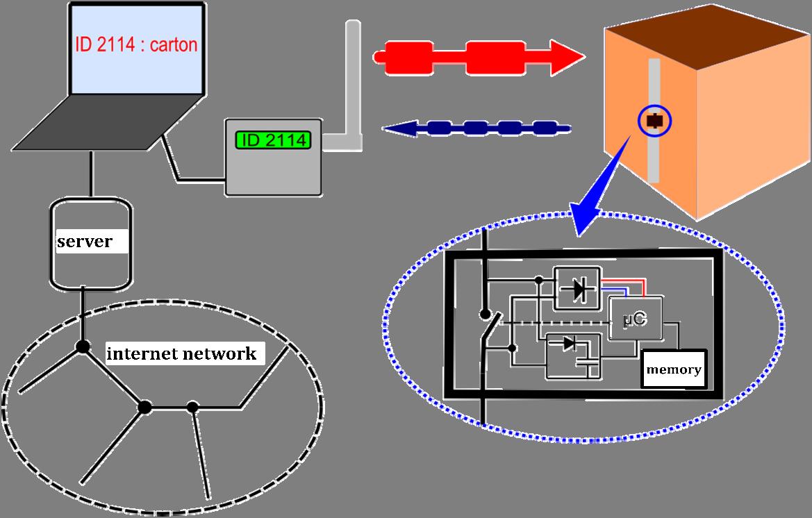
Despite the incredible number of technological parameters that make up the current RFID systems, the operating principle can be described in a general way. An RFID system is composed of one or several RFID readers, connected or not to supervising computers, which can create a link with databases. These readers allow the identification of objects due to RFID tags that are attached to them, as shown in Figure 1.2.
From an application perspective, we refer to an open system when the tag ID is universal and the association between the ID and the object can be found on a remote server (see Figure 1.2). The barcode is a well-known
Figure 1.2. Operating principle of an RFID system
example of an open system, which allows the identification of articles in a universal way. Closed systems are dedicated to applications in which ID management is carried out internally and is not externally accessible. Thus, the network infrastructure of closed circuits stops at a local network gathering information in a private database. The use of closed systems is justified sometimes by the need for a higher level of security. In this case, IDs must not be known to the public to avoid data tampering.
An RFID tag is composed of an antenna designed to operate in a given frequency band, connected to an electronic chip. A matching circuit is necessary in some cases to match the impedance of the antenna to that of the chip.
In an electronic chip, we generally find:
– an energy harvester circuit achieved with the aid of a diode rectifier;
– an asynchronous demodulator or a diode envelope detector for the reception of queries from the reader;
– a microcontroller for the processing of queries, cryptography and the preparation of responses;
– a memory that can contain the tag ID and other information specific to the application;
– an electronic switching circuit, which allows the modulation of the complex impedance of the tag in order to generate a response.
RFID tags can be classified according to their power supply mode, their operating frequency, their cryptographic capability, their communication protocol or even by the presence or absence of an electronic chip.
Thus, we refer to passive tags when the tag is completely powered by the electromagnetic field of the reader. Semi-passive tags use the energy of the reader to generate the response to a query from the reader. In contrast, the other elements of the chip such as the microcontroller and the memory draw their energy from a battery. Finally, an active tag is completely powered by a battery. It generates the response to the reader from its own energy using a radio frequency frontend. In this last case, the transmitting and receiving frequencies may be different. According to the operating frequencies, the
the chips implemented on this kind of tag are actually microcontrollers with sufficient memory and calculation units dedicated to cryptography. Communication rates can reach 848 kbit/s, which allows the fast reading of a significant amount of information. In the case of a passport, the identity photo of the holder can be read in a fraction of a second. The operating frequencies mainly used are 125 kHz, 134 kHz and 13.56 MHz. They belong to the industrial, scientific and medical (ISM) bands. The 125 and 134 kHz bands are reserved for applications requiring the storage of a small amount of information, and they have the advantage of a better tolerance to metal environments.
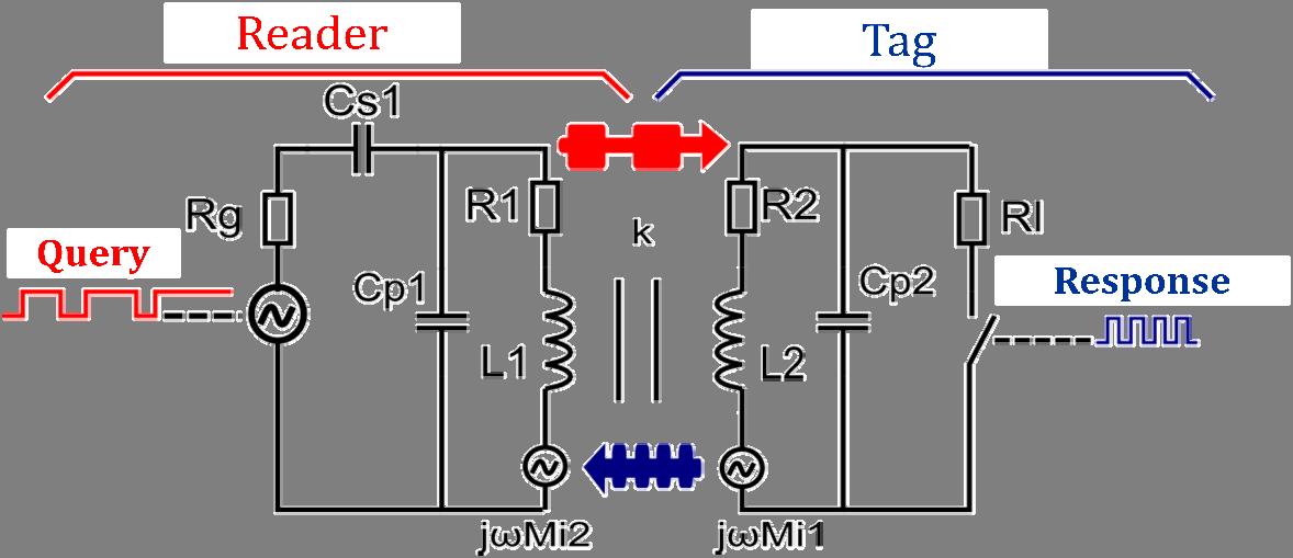
The operating principle of an RFID tag in the near-field [FIN 10] is described in Figures 1.2 and 1.4. The reader generates a continuous wave (CW), the carrier wave, for example at 13.56 MHz. The remote tag is powered by magnetic coupling, like a transformer. The energy collected by the tag is recovered through a diode bridge and powers the chip. To wake up a remote tag, the reader sends a command by modulating the carrier wave in amplitude with a modulation index of 100%. At the tag level, a simple diode detector allows the demodulation of the query from the reader. After the analysis of the query by the chip, the response of the tag is sent using the principle of load modulation.
Figure 1.4. Operating principle of an RFID tag in a magnetic coupling
To better understand the procedures that take place at the reader level during the charging of the tag module, we can make the analogy of the operation of an electrical transformer (see Figure 1.4) in which the secondary winding is connected to the primary winding by a magnetic coupling and vice versa [FIN 10, VEN 09]. If the secondary winding of the
transformer does not have a load, the secondary current is zero, which induces no opposite electromotive voltage in the primary winding. However, an electromotive force at the primary winding proportional to the level of the current in the secondary winding will reduce the total voltage at the primary winding. Thus, the current modulations at the secondary winding are, therefore, detectable at the primary winding. This is the principle used in the RFID systems in a magnetic coupling. Thus, by modulating the load at the tag level, at the rhythm of a frequency submultiple of the frequency of the carrier wave (generated by the division of the frequency of the carrier wave, 13.56 MHz), the current is modulated in the loop antenna of the tag, and by magnetic coupling, the voltage at the loop antenna level of the reader is also modulated.
The standard governing the operation of RFID tags at 13.56 MHz from the transport layer up to the application layer is ISO/IEC 14443 [FIN 10]. This standard applies worldwide. It has allowed the unification of the development of RFID systems at 13.56 MHz and has, therefore, made their use widespread in the field of transport, access control to buildings, passports and recently contactless payment methods with Paypass. Many manufacturers propose the operation of the products in the 13.56 MHz band. The coding capacities of these chips are generally between 256 bits and several tens of Kbits.
The LF systems operating mainly at 125 and 134 kHz are more heterogeneous and not part of the ISM band. Their main applications are in access control to buildings (gates) or micropayments for automatic beverage dispensing machines. For the purposes of livestock traceability and in order to fight against animal trafficking, pets are also tagged with chips at 125 or 134 kHz.
1.3.3. UHF and SHF technologies
RFID technologies in the UHF and SHF bands have emerged in the last decade and are generating a real interest, in particular since the definition of the Electronic Product Code (EPC) standard by the Auto-ID Center in 2003. The EPC brings together a consortium of 120 major companies in the field of identification and RFID technologies. To name just a few, the intended applications concern the traceability of goods or the management of pallets in logistics centers. The EPC standard has been adopted by the ISO for the
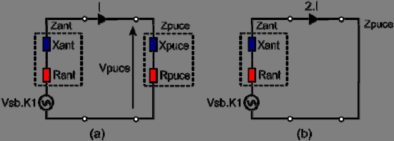
matching problems between the chip and the antenna. Figure 1.6 represents the equivalent circuit that models the energy transfer between the chip and the antenna in the case of matching (Figure 1.6(a)) and modulation by a short-circuit (Figure 1.6(b)). In order to maximize the energy transfer of the tag antenna to the chip (or the load), a complex conjugated matching should be performed [1.2]–[1.3]:
Figure 1.6. a) Matching of the antenna to the chip in unmodulated mode; b) equivalent circuit when the chip is modulated (short-circuit in parallel – Rmod = 0). The current in Rant is two times more important
In the case of a complex conjugated matching, half of the energy is dissipated in the chip, the other half is dissipated in the resistance of the antenna, which in general is composed of two parts, a radiation resistance and a resistance that models the losses in the antenna (joule loss and dielectric loss).
When the chip modulates the carrier wave to generate the response to the reader, in a first approximation, we can consider that the input impedance of the chip is loaded by a transistor operating in blocked/saturated mode. When the transistor is saturated, there is no more energy transfer to the chip and the power captured is completely backscattered in the open space. The current flowing in Rant is 2 times higher than the case of a perfect matching, which translates into a 4 times greater backscattering power in the case of a matching [1.4] (see Figure 1.6(b)). In fact, in the case of a passive tag, to
Zchip
Xchip
Rchip
Zchip
Vchip
avoid deenergizing the chip in this configuration, we use a low impedance state rather than a short-circuit.
The principle of response generation of the tag to the reader is, therefore, based on the variation of the backscattering power between two quite distinct states. A logic state “1” is characterized by a continuous wave reflected with an amplitude of up to 4 times greater than a logic state “0”. The base station, therefore, detects a signal modulated in amplitude, whose variation depends directly on the variation of the impedance state. For non-battery-assisted passive tags, we avoid in general the short-circuit state in the strict sense, to maintain a minimum of energy transferred to the chip during the response. Thus, the Rmod resistance in Figure 1.5 can have a value of approximately a hundred ohms.
The tag antenna is a key element that directly affects the reading range in the same way as the activation power of the chips. The important parameters to evaluate during the design of an antenna of an RFID tag are:
– the efficiency;
– the matching;
– the radiation pattern;
– the variation of the radar cross-section (RCS) between the two impedance states (Delta RCS).
The antenna design must, therefore, take into account these parameters, the size constraints and the environment of use. In most cases, these impose performance limits [PER 12, PER 14]. The increase in the reading range of the tag is a function of the antenna gain. However, a high gain is hardly feasible in compact dimensions. In addition, increasing the gain is achieved at the cost of the antenna aperture, which risks becoming too directive and, therefore, hardly detectable according to the orientation, and the positioning of the tag. In practice, most of the time, we search for an omni-directional behavior. As previously stated, a condition of complex conjugated matching must be carried out between the antenna and the chip. In practice, for cost reasons, the matching is carried out at the antenna level without using a
matching circuit, so that it can be connected directly to the chip. Finally, the radiation pattern of the antenna should respect the constraints of the tag usage. In general, antennas of RFID tags have an isotropic radiation in the H plan, to ensure their detection regardless of the direction of the incident field.
To establish a link budget, we can use Friis equation [1.5] that takes into account the characteristics of the transmitter, the receiver and the free space attenuation as a function of the operating frequency and distance, everything in the far-field approximation.
Prx and Ptx represent the powers at the receiver and transmitter level, and Grx and Gtx represent the gains achieved by the receiving and transmitting antennas, which take into account the potential losses due to mismatching. R represents the distance of the reader/tag, and λ is the wavelength in free space. Equation [1.5] can be reformulated in [1.6] in order to show the maximum equivalent isotropically radiated power Ptxeirpmax which is a regulated figure and whose value depends on the used ISM band (see Table 1.2). In a passive tag remotely powered by the electromagnetic field of the reader, the criterion that limits the detection range of the tag is primarily linked to the minimum activation power of the chip [PER 12]. The receiver at the reader level is generally very sensitive, as it is more evolved and has an energy source. The reason is primarily technological. A silicon chip needs voltage and a minimum current to operate its internal logic (transistors, diodes, etc.). For example, Impinj Monza 4 (IMP) chips can operate in the 860–960 MHz frequency range with a minimum power of Prx min = –20 dBm (10 µW) (read) and –16 dBm (25 µW) (write). We can thus draw a table comparing the reading range of passive RFID tags in the case of a perfect matching of the tag antenna with the chip, by taking into account the maximum permitted transmitting powers. Starting from equation [1.6], we can express R [1.7] as a function of Prx min, which corresponds to the activation power of the chip, of Ptx eirp max and of the receiving antenna gain for a given frequency. Equation [1.8] allows us to calculate R based on
Ptxerp max, the radiated power relative to a dipole λ/2. In this expression, 1.64 represents the directivity of the dipole λ/2.
The reading ranges presented in Table 1.2 are theoretical and represent a maximum value, which can be achieved in the ideal case (perfect matching between the chip and the antenna, no reflection, not a noisy environment, etc.). In a practical operating case, i.e. in actual conditions, these values can easily be divided by a factor of several units [PAR 09].
Table 1.2. Theoretical reading ranges for different chips according to usage frequencies
When more important reading ranges are required, we can add a battery at the tag level to supply power only to the digital part (microcontroller and memory). The modulation stage remains the same. The backmodulation principle is, therefore, always used. Sometimes, we call this variant “batteryassisted passive tag” or even “semi-passive tag”. To determine the reading range, we must take into account in this case the downlink (reader to tag)
and the uplink (tag to reader). It is possible in this case that the tag is activated by the reader, but that the backscattered signal is too low for the reader to be able to interpret it. In order to determine the detection ranges in this case, it may be interesting to use the RCS of the antenna, which is a parameter that is linked to its geometry on the one hand (structural mode), and to its load (antenna mode) on the other hand [HAR 64]. RCS represents the area equivalent to the area which would capture the density of the power transmitted by a source located in the far-field at a distance R and which would retransmit it in the entire space [BAL 05]. Under far-field approximation, the expression of the RCS is given by [1.9].
In this equation, Wi represents the power density that arrives at the target (or the tag) level. This power density is transmitted by a source located at a distance R. Ws is the power density backscattered by the target in a given direction. The far-field condition is valid if [1.1] is verified. In order to perform a power budget as a function of the RCS, we can use the radar equation [1.10], which allows us to calculate the reflected power at the source level by a target located at a distance R. Gtx and Grx are the receiving and transmitting antenna gains, and σ represents the RCS in meters.
The RCS value is related to the tag antenna gain in a given direction. Formula [1.11] allows us to make the link between the antenna gain and RCS when the load is matched. Equation [1.12] allows us to obtain the RCS value when the load is in short-circuit. Thus, we note that the ratio of 4 between these two load impedance states is already highlighted by the relationship [1.4].
constraints, the cost and the transmitter autonomy. These constraints are often more important than the regulatory limits on radiated power. In Table 1.4, we have gathered theoretical range values for tags by applying Friis formula for the “tag to base station” link. The reception sensitivity used is –70 dBm.
1.7. Communication diagram of an active RFID tag. Communication between the base station and the tags or directly between tags
Table 1.4. Theoretical reading ranges for active tags (Prxmin = –70 dBm)
Figure