No part of this publication may be reproduced or transmitted in any form or by any means, electronic or mechanical, including photocopying, recording, or any information storage and retrieval system, without permission in writing from the publisher. Details on how to seek permission, further information about the Publisher’s permissions policies and our arrangements with organizations such as the Copyright Clearance Center and the Copyright Licensing Agency, can be found at our website: www.elsevier.com/ permissions.
This book and the individual contributions contained in it are protected under copyright by the Publisher (other than as may be noted herein).
Notices
Knowledge and best practice in this field are constantly changing. As new research and experience broaden our understanding, changes in research methods, professional practices, or medical treatment may become necessary.
Practitioners and researchers must always rely on their own experience and knowledge in evaluating and using any information, methods, compounds, or experiments described herein. In using such information or methods they should be mindful of their own safety and the safety of others, including parties for whom they have a professional responsibility.
To the fullest extent of the law, neither the Publisher nor the authors, contributors, or editors, assume any liability for any injury and/or damage to persons or property as a matter of products liability, negligence or otherwise, or from any use or operation of any methods, products, instructions, or ideas contained in the material herein.
Library of Congress Cataloging-in-Publication Data
A catalog record for this book is available from the Library of Congress
British Library Cataloguing-in-Publication Data
A catalogue record for this book is available from the British Library
ISBN: 978-0-08-102584-0
For information on all Woodhead publications visit our website at https://www.elsevier.com/books-and-journals
Publisher: Matthew Deans
Acquisition Editor: Kayla Dos Santos
Editorial Project Manager: Emma Hayes
Production Project Manager: Joy Christel Neumarin
Honest Thangiah
Cover Designer: Miles Hitchen
Typeset by SPi Global, India
Contributors
Stefano Ambrogio IBM Research-Almaden, San Jose, CA, United States
Y. Ando Tohoku University, Sendai, Japan
G. Bersuker The Aerospace Corporation, Los Angeles, CA, United States
Chong Bi Department of Materials Science and Engineering; Department of Electrical Engineering, Stanford University, Stanford, CA, United States
Philippe Blaise CEA LETI Minatec Campus, Grenoble, France
B. De Salvo CEA-LETI Minatec Campus, Grenoble, France
Jonas Deuermeier CENIMAT/i3N, Department of Materials Science, Faculty of Sciences and Technology, Universidade NOVA de Lisboa and CEMOP/UNINOVA, Campus de Caparica, Caparica, Portugal
Regina Dittmann Peter Grünberg Institute (PGI-7), Forschungszentrum Jülich GmbH and JARA-FIT, Jülich, Germany
T. Endoh Tohoku University, Sendai, Japan
S. Fukami Tohoku University, Sendai, Japan
D.C. Gilmer Nantero, Inc., Woburn, MA, United States
Ludovic Goux Imec, Kapeldreef, Leuven, Belgium
T. Hanyu Tohoku University, Sendai, Japan
Michel Harrand CEA LETI Minatec Campus, Grenoble, France
Susanne Hoffmann-Eifert Peter Grünberg Institute (PGI-7), Forschungszentrum Jülich GmbH and JARA-FIT, Jülich, Germany
Hyunsang Hwang Department of Materials Science and Engineering, Pohang University of Science and Technology, Pohang, South Korea
Cheol Seong Hwang Department of Materials Science and Engineering, and InterUniversity Semiconductor Research Center, Seoul National University, Seoul, South Korea
Daniele Ielmini Dipartimento di Elettronica, Informazione e Bioingegneria, Politecnico of Milan and IU.NET, Milan, Italy
S. Ikeda Tohoku University, Sendai, Japan
Asal Kiazadeh CENIMAT/i3N, Department of Materials Science, Faculty of Sciences and Technology, Universidade NOVA de Lisboa and CEMOP/UNINOVA, Campus de Caparica, Caparica, Portugal
H. Koike Tohoku University, Sendai, Japan
Yunmo Koo Department of Materials Science and Engineering, Pohang University of Science and Technology, Pohang, South Korea
Luca Larcher Applied Materials, Reggio Emilia, Italy
Seokjae Lim Department of Materials Science and Engineering, Pohang University of Science and Technology, Pohang, South Korea
Massimo Longo CNR—Institute for Microelectronics and Microsystems—Unit of Agrate Brianza, Italy
Y. Ma Tohoku University, Sendai, Japan
Stephan Menzel Peter-Grünberg-Institut (PGI-7), Forschungszentrum Jülich GmbH and JARA-FIT, Jülich, Germany
Rivu Midya Department of Electrical and Computer Engineering, University of Massachusetts, Amherst, MA, United States
Thomas Mikolajick NaMLab gGmbH; Institute of Semiconductors and Microsystems, TU Dresden, Dresden, Germany
Gabriel Molas CEA LETI Minatec Campus, Grenoble, France
Cécile Nail CEA LETI Minatec Campus, Grenoble, France
H. Ohno Tohoku University, Sendai, Japan
Andrea Padovani Applied Materials, Reggio Emilia, Italy
Jaehyuk Park Department of Materials Science and Engineering, Pohang University of Science and Technology, Pohang, South Korea
Paolo Pavan Dipartimento di Ingegneria "Enzo Ferrari", Università di Modena e Reggio Emilia, Modena, Italy
L. Perniola CEA-LETI Minatec Campus, Grenoble, France
Francesco Maria Puglisi Dipartimento di Ingegneria "Enzo Ferrari", Università di Modena e Reggio Emilia, Modena, Italy
Mingyi Rao Department of Electrical and Computer Engineering, University of Massachusetts, Amherst, MA, United States
Noriyuki Sato Department of Materials Science and Engineering; Department of Electrical Engineering, Stanford University, Stanford, CA, United States
H. Sato Tohoku University, Sendai, Japan
R. Shirota National Chiao Tung University, Hsinchu, Taiwan
Jeonghwan Song Department of Materials Science and Engineering, Pohang University of Science and Technology, Pohang, South Korea
D. Suzuki Tohoku University, Sendai, Japan
Navnidhi Kumar Upadhyay Department of Electrical and Computer Engineering, University of Massachusetts, Amherst, MA, United States
D. Veksler The Aerospace Corporation, Los Angeles, CA, United States
E. Vianello CEA-LETI Minatec Campus, Grenoble, France
Shan X. Wang Department of Materials Science and Engineering; Department of Electrical Engineering, Stanford University, Stanford, CA, United States
Zhongrui Wang Department of Electrical and Computer Engineering, University of Massachusetts, Amherst, MA, United States
Rainer Waser Peter-Grünberg-Institut (PGI-7), Forschungszentrum Jülich GmbH and JARA-FIT, Jülich; Institut für Werkstoffe der Elektrotechnik (IWE 2), RWTH Aachen, Aachen, Germany
J. Joshua Yang Department of Electrical and Computer Engineering, University of Massachusetts, Amherst, MA, United States
1 OxRAM technology development and performances
Ludovic Goux Imec, Kapeldreef, Leuven, Belgium
1.1 Introduction
1.1.1
1.1.1.1
Nonvolatile memory applications
Storage-class memory (SCM)
In today’s computational systems, memories are categorized into volatile memory and nonvolatile memory (NVM) technologies.
Due to the ever increasing demand for more memory capacity, planar NAND Flash has been scaled down to below 20-nm feature size. Concomitantly, three-dimensional (3D) vertical NAND Flash has been developed as a Bit-Cost-Scalable (BiCS) solution and allows today entering the Terabyte era. As a result, the NVM market is by far dominated by NAND Flash technology, and the forecast is that the future of NAND will be NAND [1].
In the volatile memory category, the main technologies are the static RAM (SRAM) and dynamic RAM (DRAM), which are higher-speed and higher-performance technologies, however, exhibit poor scalability. Their role in a central process unit (CPU) is to store data that require immediate access while NAND Flash or hard-disk drive (HDD) store information that is not required immediately but for available future usage [2]
The problem arises when transferring data from DRAM to NAND: the overall performance of the system is limited by the huge latency gap between these two technologies. This gap has been virtually fitted with architectural solutions to increase the data access speed but at the expense of complex system design and increased chip area. In recent years, researchers have started exploring the possibility of novel memory concepts to improve the existing memory hierarchy. The concept of storage class memory (SCM) has been proposed, aiming to fill the access time gap between the “memory-memory” and the “storage-memory.”
As a “bridge” technology between DRAM and Flash, the main requirements for SCM are intermediate between DRAM and Flash and should be cost effective.
In short, SCM should be enabled by a nonvolatile, cheap, and scalable technology having clearly better reliability (write endurance and retention) than Flash. At the lead in this future booming market, Intel-Micron announced the 3D X-point Memory in 2015 [3] and launched products in 2017. Although not officially confirmed by IntelMicron, it is generally agreed in the memory community that 3D X-point is based on phase-change memory technology.
As will be detailed in the following sections, the filamentary resistive RAM (RRAM) technology has also proven to be a promising candidate in this growing market.
1.1.1.2 Internet of Things (IoT)—Embedded memory
Another booming market is the concept of Internet of Things (IoT), which is defined as “intelligent connectivity of smart devices by which objects can sense one another and communicate” [4].
The advent of billions of connected devices is creating new opportunities and huge markets for the emerging memories. In fact, the market for IoT devices has been projected to more than 3.5 trillion in 2020.
In a typical electronic system, logic and NVM components are fabricated separately due to the incompatibility in integration flow. To accommodate the exponential growth of IoT devices, chip costs have to be reduced.
This drives the need for developing new embedded memory technology where a chip can contain both logic and memory components to lower the cost and save space on the printed circuit boards. This is referred to as system-on-a-chip (SoC). The existing SoC chip uses NOR Flash as embedded memory. However, to integrate embedded NOR Flash in 28 nm node and below, up to 15 extra photomasks need to be added in the overall fabrication process, which makes embedded NOR Flash an extremely expensive technology, all the more for more advanced logic nodes. Therefore, an alternative CMOS-compatible and low-cost embedded memory technology would be highly desired to feed the IoT market as well as other embedded markets.
In this respect too, the RRAM technology is a strong contender, as will be shown next.
1.1.2 Resistive RAM technology
To fulfill the requirements of these new applications, various new memory device concepts have been proposed and studied. The prominent concepts are spin-transfer torque magnetic RAM (STT-MRAM), phase-change RAM (PCRAM), and RRAM or ReRAM. These technologies, due to limited maturity, are categorized as emerging memories.
The RRAM category is the name of a group of memory technologies characterized by an electrically reversible resistive switching functionality between a low resistance state (LRS) and a high resistance state (HRS). One of the most attractive advantages of RRAM is the low-cost integration allowed by the combination of CMOS-friendly materials within a simple two-terminal device structure, which typically consists of a dielectric layer sandwiched between two metal electrodes.
Between the numerous mechanisms potentially at the origin of resistive-switching effects, nano-ionic transport and redox-reaction mechanisms taking place at the nanometer scale [5] have been clearly identified as accounting for the switching functionality of various systems.
In most of the RRAM devices reported [6–8], the resistive switching property originates from the growth and shrinkage of a nanoscaled conductive filament (CF) in the
dielectric layer. These devices are generally referred to as filamentary RRAM devices, whose characteristics mainly depend on the CF. In particular, due to the nanoscale character of the switching, filamentary RRAM has been so far perceived as highly scalable [5,9], and has thus been developed intensively.
This is, for example, the case of electrochemical metallization memory (ECM) and valence change memory (VCM) cell concepts.
The ECM concept has led to the development of the conductive bridge RAM technology (CBRAM), whereby the filament consists of metallic species injected from an active electrode, typically Ag or Cu, into the dielectric layer [10]
On the other hand, the VCM concept is at play in the Oxide switching RAM technology (OxRAM), whereby the dielectric layer is an insulating oxide material through which a CF of oxygen-vacancy defects (Vo) is electrically created [11]. This technology generally uses a transition metal oxide (TMO) material, typically HfO2, Ta2O5, or TiO2 [11,12].
On the other hand, devices with nonfilamentary resistive switching mechanism have also been reported [13,14]. These devices exhibit area-dependent current flow, which is not observed in filamentary RRAM after the filament has been created. Here the resistive switching is achieved by modulation of the effective tunneling barrier thickness at the oxide-metal interface, as induced electrically by the uniform motion of Vo defects. An advantage of this concept is the scalability of the operating current with the device area.
Between these different concepts, this chapter is dedicated to the filamentary OxRAM technology, and we specifically focus on the works achieved at imec in this field over the last decade.
In Section 1.2, we first review how the initial developments moved from the unipolar to the bipolar switching concept, and we describe typical structures, fabrication flows, testing procedures, and electrical characteristics of bipolar devices that mainstream nowadays.
In Section 1.3, we focus on material developments allowing substantial improvements in memory performances, and finally, in Section 1.4, we address key reliability challenges to address in the future.
1.2 History and basics of filamentary OxRAM
Resistive switching and negative differential resistance phenomena were first reported in the 1960s in rather thick oxide materials, for example, Al2O3 [15] and NiO [16] layers. This early period of research has been comprehensively reviewed in Refs. [17,18].
Since the 2000s, there has been a renewed interest in resistive switching in TMO systems, driven by the potential industrial application as RRAM. In this period, the developments focused on NiO and TiO2 systems exhibiting unipolar switching operation [19,20], which means that the same voltage polarity may be used both for set switching to LRS and reset switching to HRS. This unipolar operation received large consideration due to possible integration with a two-terminal selector element, such as
a diode, which in turn held the promise of dense memory integration potential. Goux and Spiga [19] give a recent review of unipolar-switching developments.
1.2.1 From unipolar to bipolar concept
The unipolar switching originates from a distinct class of switching mechanism, which is called thermochemical memory (TCM) mechanism. Indeed, contrary to bipolar VCM switching mechanisms where the motion of oxygen ionic species is dominated by drift, the TCM switching is dominated by thermal-controlled diffusion and redox reaction of active oxygen species.
This major microscopic difference between VCM and TCM mechanisms reflects in different memory characteristics.
1.2.1.1 Unipolar operation mechanism
Unipolar switching is usually observed in simple metal–insulator–metal (MIM) structures, where the “I” and “M” elements are typically constituted of an oxide layer and noble metallic layers respectively.
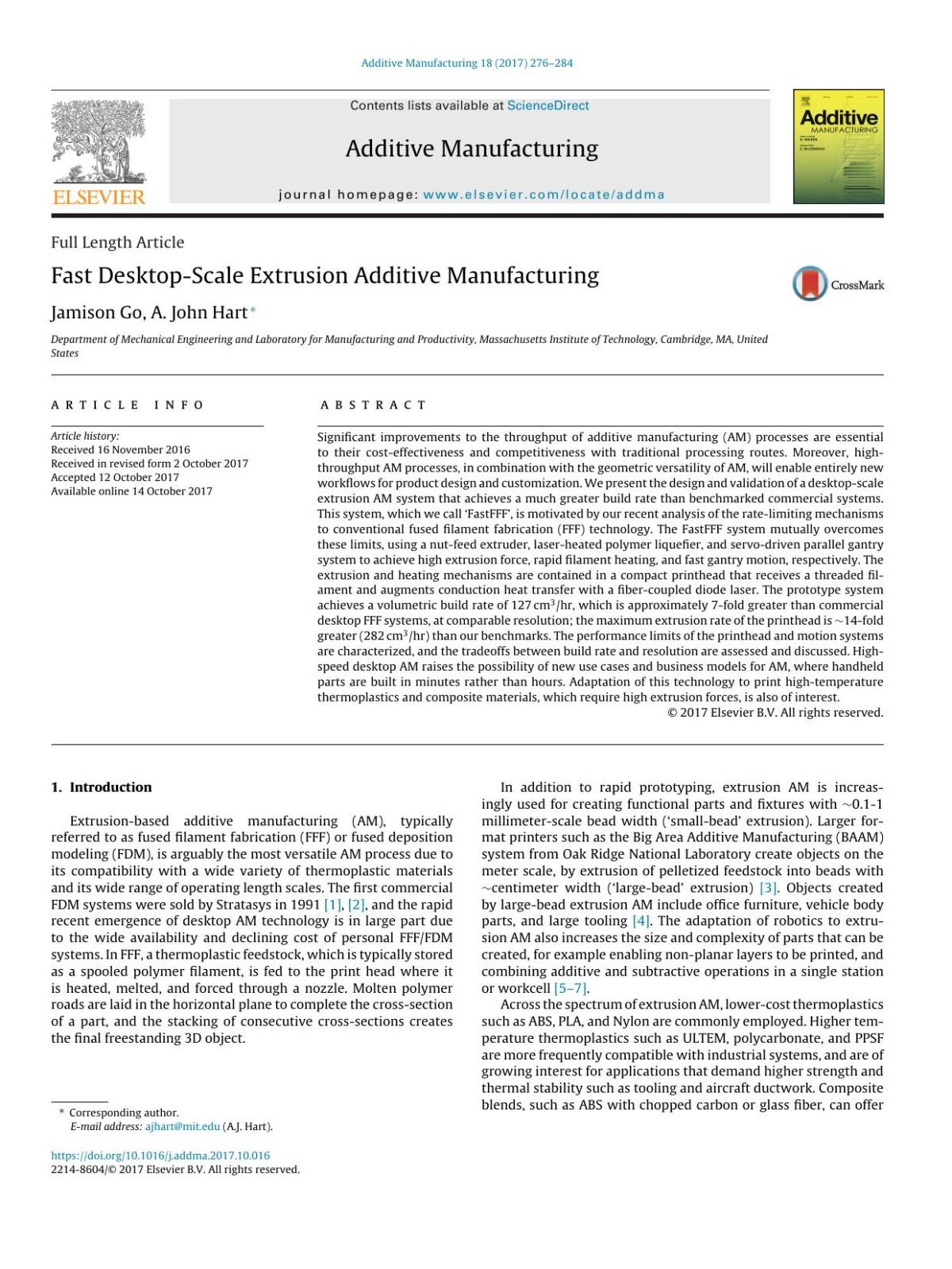
Fresh cells are most often in a very high resistive state requiring the application of a large “forming” voltage (Vf), which is generally regarded as a sort of electricalbreakdown [21,22] allowing to turn the cell for the first time in LRS. After this socalled “forming” conditioning step, the cell may be reversibly reset-switched to HRS and set-switched to LRS, as illustrated in Fig. 1.1A–C.
The reset switching operation corresponds to the rupture of the CF, resulting in a drop of conductivity. Let us assume first that the CF consists of a VO-chain. Upon reset operation, the current density through the CF has been shown to reach high values, generating the necessary thermal energy to activate the migration of oxygen from O-rich regions outside the CF toward O-deficient regions inside the CF. According to this picture, the reset switching corresponds to the local reoxidation of the CF. It requires moving back the forming-generated O-species to VO sites, and as the switching is unipolar in nature, this process is expected to take place primarily laterally by diffusion mechanisms. In agreement with this scenario, we have evidenced by means
Fig. 1.1 (A) Cross-sectional TEM images and (B) schematic structures of Ni\NiO\Ni cells; (C) Consecutive unipolar I-V sweeps obtained on the same cell; (D) Extracted Vset and Vreset as a function of the I-V cycles [21].
of TEM and EELS characterization a significant increase of the O/Ni ratio after reset operation in TiN\NiO\Ni cells [23]. Assuming now that the CF consists of a metallic Ni-chain the thermal dissolution of Ni upon reset switching might be a more realistic mechanism for CF rupture. In this scenario too the diffusion mechanism is expected to occur sideways from inside the Ni-rich CF toward outside Ni-poor regions. In both situations, the physics of the reset operation is overall expected to depend on the spatial distribution of defects, on local fields as well as on temperature profiles.
1.2.1.2 Variability and endurance of unipolar switching
Some NiO cells have been reported to exhibit coexistence of unipolar and bipolar resistive switching properties [21]. While NiO is intrinsically a thermochemical material, the disordered/defective microstructure of the layers proved favorable to ionic drift and electrochemical redox mechanisms, allowing thus selecting reversibly any switching mode between unipolar and bipolar [21]. Note that the forming step itself is sufficient to induce disorder and facilitate ionic drift in high-quality dielectrics. For example, coexisting unipolar and bipolar operation modes were obtained after forming operation in TiN\HfO2\Pt cells where a high-quality amorphous HfO2 layer was prepared by ALD [11,24].
The switching variability was investigated in various reports [20,21]. In general, the switching-voltage distribution is wider for unipolar than for bipolar switching. Indeed, as the reset mechanism is a self-accelerated process for unipolar mechanisms, it may be argued that the programming of the HRS state is difficult to control, leading to different cycle-to-cycle (C2C) RHRS and subsequent Vset parameters, as observed in Fig. 1.1D [21]. Other reports also suggested that the variability degrades in a configuration of multiple-CF network [25], wherein the switching “hot” spot is likely to move within the network from cycle to cycle.
Hence, not surprisingly, write-endurance lifetime is clearly shorter for unipolar than for bipolar switching. Between the invoked origins are the larger temperatures required for reset compared to bipolar switching, possibly inducing electro-migration effects [26], the gradual loss of species involved in the radial diffusion, or simply the drift-induced loss of species inherent to the use of a single programming polarity [11].
Overall, unipolar OxRAM suffered from high operating voltage, large switching variability, as well as limited endurance. Hence, it gradually lost interest concomitantly with the substantial improvement of bipolar OxRAM technologies by the years 2010.
Nowadays, modern OxRAM devices are implemented in bipolar mode where the growth or shrinkage of the conductive filament is achieved by relying on a voltage controlled ion migration assisted by temperature and electric field enabling faster set and reset operations. The rest of the chapter will be dedicated to the development of this concept.
1.2.2
1.2.2.1
Bipolar switching concept
Device structure
In addition to memory performance limitations, unipolar switching OxRAM showed the major drawback of involving difficult-to-integrate materials, for example, noble
metals required in the model system Pt/NiO/Pt to avoid parasitic oxidation during the thermal-induced reset operation.
In contrast, the drift-dominated mechanisms involved in bipolar VCM allow using CMOS-friendly electrode materials like TiN or TaN.
Regarding the oxide layer, excellent performances have been demonstrated using mature atomic-layer deposition (ALD) oxide layers like HfO2 [7,27] or Ta2O5 [28,29], which are considered today as the mainstream oxide families of OxRAM.
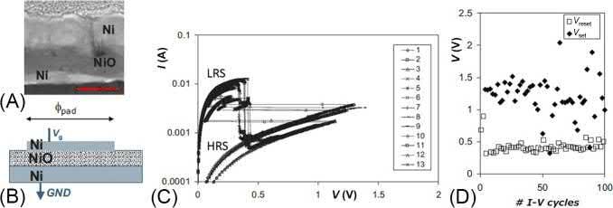
However, the key success of bipolar OxRAM lies elsewhere, that is in the electrical asymmetry of the structure, as required for a bipolar functionality. We evidenced by Internal Photoelectron Emission (IPE) that some low work-function metallic layers like Hf, Ti, Ta inserted at one interface of the MIM stack are very appropriate to induce such required asymmetry. Fig. 1.2 shows the substantial decrease of electron barrier of ~1 eV from TiN to Hf electrode [30]. This effect is due to the oxygen scavenging by Hf leading to the development of an oxygen deficient hafnia interlayer between Hf and HfO2. A resulting substochiometric oxide interlayer is formed, often referred to as oxygen-exchange-layer (OEL) [31]. The role of this layer will be to “exchange” oxygen species with the filament in the oxide layer during the bipolar switching operation. On the other hand, the TiN opposite electrode is considered inert to oxygen in the first approximation. Hence, the O-scavenging layer of Hf induces an oxygen vacancy profile along the oxide thickness and will be the main knob allowing to tune the bipolar switching functionality and characteristics of the device. Both the nature and the thickness of this layer will be key to the device performances, as will be shown in the following sections.
As best O-scavenging materials, in general, the use of “mother” metals in Ta2O5\ Ta [29] or HfO2\Hf [27] is preferred and shows robust stack stability after integration thermal budget. And in practice, up to today the TiN\HfO2\Hf\TiN and TiN\Ta2O5\
Fig. 1.2 Internal Photo-Emission (IPE) characterization of TiNx/HfO2/TiNx and TiNx/Hf/ HfO2/TiNx samples, showing the logarithmic plots of the electron quantum yield as a function of photon energy. The signal observed under positive +1 V and negative 1 V bias corresponds to electron IPE from the bottom and top metal electrode, respectively [30]
Ta\TiN are considered as mainstream OxRAM devices and will be the baselines discussed in the following sections.
1.2.2.2
Integration and scaling
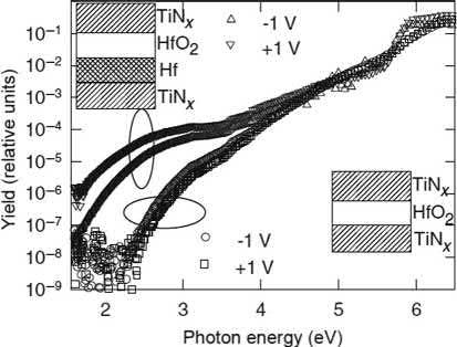
In this section, we describe a typical 1-Transistor/1-Resistor (1T1R) integration flow used to fabricate TiN\HfO2\Hf\TiN and TiN\Ta2O5\Ta\TiN in a crossbar configuration, and where the “T” element is the selector device addressing the “R” OxRAM device (Fig. 1.3A).
After the front-end-of-line (FEOL) processing of this select transistor (nMOSFET), the OxRAM device is fabricated as follows: A 100-nm-thick TiN is deposited by physical-vapor-deposition (PVD) as a bottom electrode (BE) where the electrical connection to the transistor is realized by tungsten (W) plugs. After BE patterning SiO2 is deposited and polished by chemical–mechanical polishing (CMP) down to the TiN surface. This step ensures flat BE surface and is thus critical for device performance. Subsequently, the active HfO2 layer, or Ta2O5 respectively, is deposited by ALD, typically using HfCl4, or TaCl5 resp., as precursor, and H2O as the oxidant, followed by the PVD of the Hf, respectively. Ta, O-scavenging metal layer and a TiN top electrode (TE). Then, the oxide\TE stack is patterned via lithography and etch steps, where a typical device size of 40 × 40 nm 2 is formed in imec process flow. Finally, passivation modules using Si3N4 and SiO2 layers deposited by CVD and contact formation steps are carried out.
Fig. 1.3B depicts the cross-section TEM image of a pristine TiN\HfO2\Hf device. By means of patterning trimming processes, sub-10 nm devices are realized. As observed on Fig. 1.3B the Hf layer is laterally oxidized during process flow, which reduces further the active device size [27].
1.2.2.3 Typical device testing and characteristics
The role of the select transistor is not only to isolate and address the cell but also to limit more efficiently the current overshoot during forming and set, as compared to the
Fig. 1.3 (A) Schematic representation of the so-called 1T1R configuration; (B) cross section along BE and TE of a minimum-sized (8 × 12 nm2) reference 5 nm-HfO2\10 nm-Hf RRAM stack; the HfO2 layer is amorphous, Hf is crystalline, oxides sidewalls at TE are further reducing effective cell size; (C) typical set and reset I-V traces obtained on the cells [27]
current compliance (CC) function of a commercial semiconductor parameter analyzer (SPA) [22]. In a 1T1R scheme, the transient current flowing through the OxRAM cell is controlled by fixing an appropriate gate voltage (Vg), which is a key aspect for reliable characterization of the device because the CF properties depend on this transient current [19]
The set operation is carried out by applying a positive voltage to the selected cell Bit-Line (BL) while the Source-Line (SL) is grounded. Conversely, for reset operation, a negative voltage is applied to the BL. In a well-designed 1T1R structure with controlled stray capacitance, the maximum current reached during reset is linked to the saturation current imposed by the transistor during the set operation. In any case, in practice, larger Vg may be applied during the reset operation because this step does not need to limit the current. For state resistance readout, the transistor is fully open and Vread = 0.1 V is applied to the BL.
Using this methodology Fig. 1.3C shows typical set/reset I-V traces obtained after forming on TiN\HfO2\Hf cells and using a Vg amplitude allowing a maximum operating current Iop = 50 μA during set, as imposed by the saturation level of the transistor.
Forming
As mentioned, before memory operation the cells need to undergo a “forming” step, whereby the conductive filament is formed through the oxide layer.
In Ref. [27] we studied the scaling behavior of the forming voltage (Vf) down to 10-nm TiN\HfO2\Hf cell size. We observe that while amorphous HfO2 maintains a well-behaved scaling vs area, polycrystalline HfO2 shows abrupt dispersion and median Vf increase below ~40 nm size, which is attributed to the abrupt decrease of grain-boundary density [27]. Therefore, in order to keep Vf control with scaling to sub10 nm size, amorphous oxide layers are preferred, allowing uniform weak electrical path and controllably low Vf
We also observed that the forming operation is also highly controlled by the engineered O-scavenging layer. Fig. 1.4 shows for TiN\Ta2O5\TE cells that Vf may be drastically decreased by changing Ta to Ti TE O-scavenging layer [29]. This is due to the larger O-affinity of Ti, resulting in a lower formation energy (Ef) of Vo in Ta2O5, and which in turn induces a lower Vf. As can be observed in Fig. 1.4B, the breakdown voltage (Vbd) data extracted by applying opposite voltage polarity are higher than Vf, which is due to a larger energy required for the drift of oxygen anionic species toward TiN as compared to the O-scavenging layer.
Interestingly, a thicker Ta layer or the use of a substochiometric TaOx TE layer also allows to tune Ef and thus Vf. Actually, the nature and thickness of the scavenging layer tune the oxygen chemical potential at the interface, as will be detailed in the following sections.
Note also that the scavenging is so strong for Ta2O5\Ti cells that the top part of the Ta2O5 layer is fully depleted after integration (Fig. 1.4C) and the switching operation is poor. This effect confirms that the mother-metal Ta is preferred to preserve device integrity. Using Ta (10 nm) TE, excellent Vf uniformity is observed for a Ta2O5 thickness range down to 3 nm, which allows to controllably limit Vf < 1.5 V for device sizes down to 20 nm [29].
(15dev./test)
Fig. 1.4 Median preforming I-V traces (A), and Vf and Vbd data of 30-nm-size Ta2O5 devices having different TE materials, showing strong scavenging difference between Ta- and Tibased TE; (C) XTEM and EELS profiles on as-integrated devices, showing a huge Ti-induced O-soaking from the Ta2O5 layer [29].
Filament shape and scaling
The forming step is expected to result in a Vo-rich filamentary region having asymmetric [Vo] profile increasing from the TiN to the Hf interface [32,33]. This forming scenario is more likely to occur than the virtual-cathode growth model (growth of Vo defects from the cathode side) because the Vo formation energy (Ef) will decrease closer to the scavenging layer, resulting in larger [Vo], and the mobility of the O-anionic species will increase with the increase of [Vo][33]. Hence the filament will gradually form from the scavenging layer toward the “inert” TiN electrode. Based on this scenario, it is expected that the forming step results in a conical filament having its narrow constriction closer to TiN. Likewise, the reset switching is expected to take place “naturally” closer to the TiN anode due to: (i) the lower Vo density to recover; (ii) the O-blocking role of the TiN interface during reset-induced O-anionic drift; and (iii) the larger O-mobility within O-deficient HfO2 materials.
A few years after proposing this scenario, we performed a 3D Conductive AtomicForce-Microscopy (C-AFM) tomography experiment on a TiN\HfO2\Hf cell [34]. This technique allows, after electrical forming of the device, to record the current flowing through the scanning conductive tip while scrapping gradually the device materials. In this “scalpel” mode, the tip is brought in contact with the sample and mechanically scrapes a layer of the material to expose the layer underneath. The C-AFM imaging mode is used in-between successive scalpel steps to generate 2D images of the conduction map. After complete device scrapping, a 3D tomogram is reconstructed by interpolation of 2D images. Fig. 1.5 shows the result for TiN\HfO2\Hf cells programmed using a forming current of 50 μA. The experiment confirmed the conical shape of the filament, with its widest part near the Hf TE (7 nm) and the narrowest region near the TiN BE (3 nm), as shown in Fig. 1.5C.
Fig. 1.5 3D observation of a conductive filament by C-AFM tomography technique in TiN\ HfO2\Hf cell. (A) Tomographic reconstruction of the crossbar memory cell visualized by volume rendering after top electrode removal (scan size 800 × 200 nm); (B) 2D zoom into the region containing the CF and observation by volume rendering and isosurface at fixed threshold (blue shape) for the CF under investigation in 5-nm-thick HfO2 (scale bar 2 nm). The conductive filament is shown in double cross section (axes according to inset). The low-current contribution in the tomogram is suppressed to enhance the contrast of the highly conductive features. (C) 2D observation of the CF section-planes (left panels) and C-AFM spectra (right panels) to determine effective CF size [34].
This experiment also evidenced that OxRAM technology may be scaled below 10-nm cell size.
Set/reset switching
After forming, the OEL will serve as a Vo reservoir supplying Vo species during set switching to LRS and absorbing them back during reset to HRS. The actual set/reset operations will translate geometrically by the modulation of the constriction width close to the TiN BE, which will, in turn, modulate the electrical resistance level. Electrically, this translates, similarly to the unipolar switching, into an HRS resistance level intermediate between LRS and pristine resistance levels.
Note that only the constriction will impact the device resistance, so it should be understood that the OEL element extends from over the rest of the filament. This OEL element created during forming contains all Vo species required for set/reset operation, meaning no additional Vo defects are created.
As set/reset voltages (Vset/Vreset) drop locally on the defective constriction, their amplitude is lower than Vf. In practice, to better characterize the intrinsic switching properties, it is convenient to use a structure having an integrated load resistor as a current limiter (in a so-called 2R structure) [35]. In this scheme, we typically apply triangular pulses to one electrode of the 2R device structure. The applied voltage is acquired on one channel of a high-bandwidth oscilloscope while the current is read out by connecting the opposite electrode in series to the 50-Ω impedance-matched input resistance of the oscilloscope and converting into current the voltage generated on this shunt resistor.
Fig. 1.6 shows typical set/reset I-V curves after subtracting the voltage dropped on the load resistor. For the set switching, we observe that after overcoming a “trigger” set voltage, the voltage snap-backs to a transient Vtrans voltage, and the transient current rises at this constant Vtrans, which corresponds to the gradual growth of the constriction. Interestingly, the transient reset is onset after applying an opposite voltage having the same amplitude of Vtrans, which is followed by a voltage snap-forward due to voltage redistribution during constriction narrowing. Contrary to set, reset operation will thus be self-limited.
V trans was observed to depend neither on the operating current nor on geometrical factors [35] . Hence, V trans constitutes the intrinsic transient switching voltage parameter of the device, which we relate to the Vo mobility measure during switching. Consistently, we also observed that V trans varies in the range 0.4 –0.7 V ( Fig. 1.7 A and B) depending on the scavenging material although the constriction sits at the opposite side [29] . This effect is due to the “remote” character of the scavenging [30] , which means that the scavenging layer modulates the oxygen chemical potential up to the opposite electrode ( Fig. 1.7 C). Therefore, a strong scavenging layer, such as Hf, will lower the chemical potential and thus increase Vo mobility. In agreement, HfO 2\Hf cells exhibit lower V reset parameter than Ta 2O 5\ Ta cells [29] .
Fig. 1.6 DC cycling on 2R structure (RA = 5.68 kΩ) showing the “extrinsic” I-V trace (blue) and “intrinsic” (red), both lines are mean over 50 cycles. The abrupt current drop in “extrinsic” RESET (not observed in 1R and 1T1R structures) can be linked to voltage accelerated RESET consequence of the large overvoltage (|V-Vtrans|) already present at RESET onset [35]
Fig. 1.7 (A) DC HRS and LRS resistance, and (B) switching-voltage distributions for Ta2O5 and HfO2 devices, showing the tuning of switching parameters by the TE material, irrespective of the dielectric material; (C) Schematic representation of the oxygen chemical-potential profile along the CF, tunable by the electrodes and thus allowing modulation of the Vo mobility for fixed CF geometry (ωx) [29].
Quantum point-contact conduction and hour-glass model
We developed both a Quantum Point Contact (QPC) conduction model [36] and a so-called Hour-Glass (HG) model [37] allowing to describe the complete set of experimental electrical properties of our devices.
The QPC model is based on the Landauer-Büttiker formulation which treats the transport as a transmission problem for electrons at the Fermi level. In this approach, the conduction is controlled by the CF constriction length and width, which are inversely proportional to parameters ωx and ωy, respectively, which are determined themselves by a parabolic potential barrier along the filament and a transversal parabolic potential well, respectively, defining a saddle surface in the x, y, E-space (Fig. 1.8A). Since the transport is assumed to be ballistic inside the QPC, the applied potential drops only at the two CF interfaces of the constriction.
Using this QPC model, we have proposed an HG electrical switching model aiming to describe the atomistic movement of the ions while retaining analytical tractability. The proposed model proved successful to model the electrical switching characteristics and statistical fluctuations of our HfO2 and Ta2O5-based devices.
nc: number of Vo in constriction wy0: width parameter for I particle
Fig. 1.8 (A) Energy diagram (top) and spatial schematic drawing (bottom) of a filament, assuming many interacting Vo defects forming a conduction band; (B) schematic representation of the CF constriction made of nc defect particles and whose length and width are determined by ωx and ωy geometry parameters; (C) QPC modeling exercise of I-V traces obtained in the course of a reset operation performed on a TiN\ Al2O3\Hf (A3) cell operated at Iop = 1 μA; dots are experimental I-Vs while solid red lines are nc-dependent QPC traces [38]
This switching model consists of five major components with specific assumptions:
1. Conduction model: The current is controlled by QPC at the constriction
2. Structural model: The model calculates the number of available Vos (“absence” of oxygen ions) constituting the CF after forming. Based on this, the CF is abstracted into three reservoir systems: (i) a top reservoir (TR) extending from the OEL to the constriction interface, (ii) a bottom reservoir (BR) near the constriction and BE interface, and (iii) a current limiting constriction (C). The Vo particles may move from TR to C and to BR or the other way around, like sand moves in an hourglass so that at any time the total number of particles ntotal = nBR + nTR + nc. The number of particles in the constriction nc is the integer state variable which is related to the QPC geometrical parameters of the constriction ωx and ωy (Fig. 1.8B).
3. Kinetic model: This model describes the dynamic change of nc where four processes need to be considered: particle emission from C to TR or BR (reducing nc) and emission from TR or BR to C (increasing nc)
4. Thermal model: The temperature calculation is based on classical Joule heating applied in the maximum field zones of the CF, and is expressed as T = Tambient + α V I Rth/nc, where Rth is the effective thermal resistance of the CF. Note that the narrower the constriction, the higher the temperature increases.
5. Stochastic component: Finally, to address the stochastic character of the switching, the time constants of Vo emissions are considered as mean values of the exponential time constant distribution. A Monte-Carlo algorithm is used for the set/reset transient modeling with the inclusion of statistical variation.
In our developments and investigations, we used the QPC model for estimating the constriction geometries, and we used the HG model to estimate the local temperature, the statistical variability of the switching parameters, as well as the reliability failures.
Memory performances
During switching, the motion of oxygen species is driven by a thermally assisted drift mechanism. Thanks both to the high temperatures reached locally by the high current density flowing through the narrow constriction, as well as the very short distance required for Vo emission in and out of the constriction, set/reset operations are very fast. Typically the switching transient is in the order of the nanosecond, and the required switching time for stable filament set and reset lies in the range of a few nanoseconds [7, 29]. In Ref. [29] we showed functional switching of TiN\Ta2O5\Ta cells using voltage pulses in the nanosecond range for pulse amplitudes Vp < 2 V (Fig. 1.9A). Using these conditions >1 billion write cycles may be performed without failure (Fig. 1.9B). Similar switching and endurance characteristics may be observed on HfO2\Hf cells [7, 27,39]. In Ref. [27], we showed, however, that endurance lifetime is decreased to ~1 million cycles for devices scaled below 10 nm.
Fig. 1.9 (A) oscilloscope traces of ultra-short triangular programming pulses used to assess write endurance properties of TiN\Ta2O5\Ta devices; (B) 1e9 unverified write cycles reliably obtained using PW < 5 ns and Vp < 2 V [29].
With respect to switching energy, it may be fairly approximated by multiplying the transient current by Vtrans~0.5 V (Fig. 1.6). Hence, for an operating current of 100 μA, typical set energy and power lie in the range of ~1 pJ and 50 μW, respectively. As the maximum reset current is similar to the maximum set current [35], the reset energy is similar to the set energy.
Overall these results showing sub-10 nm scalability, low switching energy and time, as well as good endurance potential, have triggered intense development efforts to further improve device performances. The next section will detail a few aspects of key material developments.
1.3 Bipolar OxRAM material stack development
1.3.1
Optimization of the scavenging layer for retention
As mentioned in the previous section, the O-affinity of scavenging material controls the oxygen chemical potential (μo) at the interface with the oxide. In turn, it controls the forming and switching voltages [40,41]. It also affects the mobility of Vo species involved in the switching. Indeed, using the same operating conditions, stronger scavenging layer results in larger Memory Window (MW = RHRS/RLRS) (Fig. 1.7B), or alternatively lower switching voltage is observed in such case for a same resistive window.
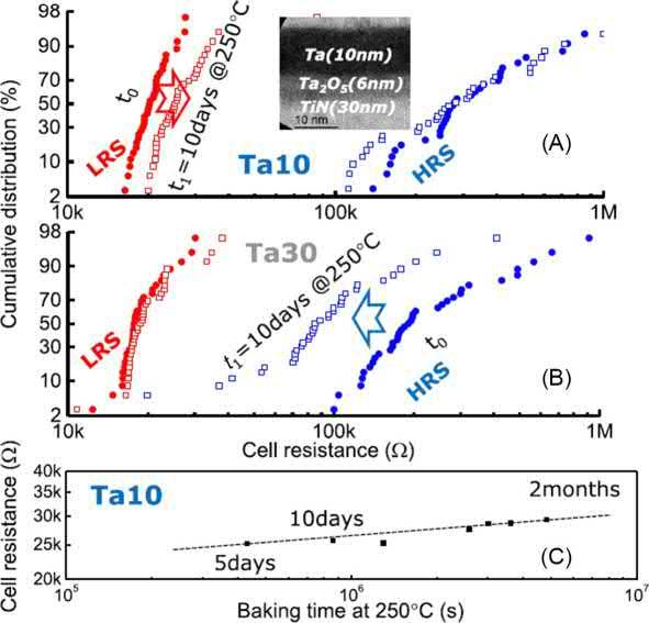
To a lower extent than the nature of the material, the thickness of the scavenging layer also allows tuning the chemical potential profile through the stack. The beneficial effect of this thickness engineering is specifically observed on the retention characteristics. In Ref. [40] we made an extensive retention study of TiN\Ta2O5\Ta cells having either 10-nm-(Ta10 cells) or 30-nm-thick Ta scavenging layer (Ta30 cells).
We observed that for 10-nm-thick Ta the LRS resistance state (RLRS) distribution has slightly shifted to larger resistances after 10 days at 250°C while the RHRS distribution has hardly moved. On the other hand, and very interestingly, for 30-nm-thick Ta the situation is reversed, meaning that it is the RHRS distribution that has shifted to lower values after baking while RLRS did not move (Fig. 1.10A and B). Both for Ta10 and Ta30 cells, the baking-time dependency of the loss followed a slow power law, such that the state distributions did not move significantly more between 10 and 60 days at 250°C (Fig. 1.10C). The power law is due to a distribution of time constants related to local fluctuations of energy barriers for defect motion.
We attributed these retention results to the modulation of μo at the CF\Ta interface by the Ta thickness. In other words, the thicker Ta layer in Ta30 cells increases slightly the heat of formation of Ta2O5 at the interface, favoring thus slightly more the CF reduction as compared to Ta10 cells, and resulting in stabilized LRS. This view is also in agreement with the slightly reduced Vf measured for Ta30.
On the other hand, oxygen drifts back to the CF during reset, which lowers the Vo concentration (Vo) closer to the TiN interface and results thus in a locally richer oxygen environment leading to larger μo. This effect thus offsets in HRS the balanced chemical profile met in LRS, leading to less stable HRS. A symmetric description holds for Ta10 cells.
Fig. 1.10 Impact of the Ta thickness on the LRS and HRS retention behaviors of TiN\Ta2O5\Ta cells, showing excellent tunability between (A) more-stable HRS (obtained for thinner Ta), and (B) more-stable LRS (obtained for thicker Ta); inset of (A) shows an XTEM image of the asintegrated Ta10 cell; (C) baking-time dependency of the median resistance of LRS distribution for Ta10 cells [40].
Importantly, these results emphasized the dominant role of the “vertical” diffusion and local redox mechanisms between the CF and the scavenging material over bulk diffusion of Vo species.
Note that a severe baking temperature of 250°C is used in Ref. [40]. When, however, a milder temperature of <150°C is used, retention stability is achieved both for LRS and HRS states on the median level, while only retention tail losses are observed. In Ref. [42] we studied the origin of tail losses for TiN\HfO2\Hf cells and confirmed that the tail bits originate from low activation-energy (Ea~0.5 eV) diffusing species, which are understood as metastable Oxygen (O)-ions moving along the CF between the constriction and the scavenging layer. We will come back to this study in Section 1.4
1.3.2 Optimization of the bottom electrode for endurance
In Ref. [43] we investigated the endurance characteristics of TiN\Ta2O5\Ta cells as a function of set/reset pulse amplitudes and pulse width. We showed that the use of a standard 10-ns-long reset pulse of 1.5 V resulted in endurance lifetime of 1 million
cycles. From this point, we showed that the increase of both the reset voltage Vreset and pulse width PWreset resulted in a drastic decrease of the lifetime, while the set pulse had a minor impact on endurance behavior [43]
On the other hand, HG simulations of the CF temperature during switching revealed that the CF temperature is much larger during reset than during set. The main reasons are as follows: (i) during set transient the voltage snap-backs to a lower standby voltage (Vtrans~0.5 V) while most of the voltage redistributes to the select transistor; (ii) the CF temperature is calculated from the power dissipation in the constriction, which consists of less nc defects in HRS than in LRS, and is thus larger in HRS, resulting in larger temperature rise during reset transient.
Furthermore, HG simulations showed large temperature fluctuations during reset, which is related to the nc fluctuations due to the competition between reset-induced Vo-emission and thermal-induced Vo-capture in the narrow HRS constriction, which also accounts for the current noise typically observed during reset and is a signature of this dynamic balance [44]
Hence, endurance lifetime appeared to be controlled by the large temperature peaks occurring during reset, and we showed it could be increased to 100 million cycles by using ns-short reset pulses of moderate amplitude [28, 43].
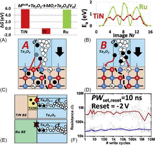
The chemical origin of the thermal-induced degradation lies in the chemical interaction between the oxide and the TiN BE. Indeed, in the previous section, we described the conical shape of the CF, having its “hot” constriction close to the TiN BE. And although TiN may be considered as an “inert” electrode for bipolar functionality demonstration, its nonideal character is revealed by endurance stress. We calculated by ab initio the free enthalpy of oxidation ΔG of BE materials by Oxygen (O) from the CF. Large ΔG ~6 eV is obtained for ideal TiN crystal, however, it drops to 2 eV for pure Ti (Fig. 1.11A). In PVD-deposited TiN layers, any point defects, such as nitrogen vacancies (VN) or Ti dangling bonds will have the same effect of locally decreasing ΔG and will result in TiN oxidation.
Hence, gradual TiN oxidation by these microscopic mechanisms is likely induced by the large reset field and temperature during endurance, leading finally to failure to set (failure B in Fig. 1.11) due to difficult O-detrapping from TiN, which is the failure mode observed for “strong” reset conditions.
On the other hand, endurance stress using “softer” conditions with lower reset field and temperature may be insufficient for TiN oxidation, however, sufficient for O in-diffusion as interstitials within TiN or simply through defects like grain boundaries, which would lead finally to failure to reset (failure A in Fig. 1.11).
From ab initio, the use of a Ru BE would result not only in restored large ΔG but also in reduced O in-diffusion (Fig. 1.11B), which should improve the immunity to failures B and A, respectively. Note that the crystal structures used in the calculation for Ru are hexagonal closed packed and cubic for TiN. In agreement, experimental endurance tests on Ru\Ta2O5\Ta devices confirmed the ab initio predictions, as shown in Fig. 1.11F. In Ref. [28] we showed further that even for large temperatures and fields associated with a reset pulse of 2.3 V, no failure was observed before 1 billion endurance cycles.
Using the same reasoning, the use of oxide materials having a lower enthalpy of metal oxidation is predicted to result in improved robustness to O-injection into the
Fig. 1.11 Ab initio calculation of the energy barrier required for O (A) to react (ΔG) with BE materials and (B) to diffuse (Ea) in TiN and Ru; (C) and (D) schematics describing possible degradation mechanisms accounting for failure modes A and B, where O is shown in black. (E) Schematics depicting suppressed O-induced BE degradation during switching using Ru. (F) Endurance characteristics obtained on Ru\Ta2O5\Ta devices tested in standard condition except for Vreset = 2 [43].
BE material. As expected, TiN\HfO2\Hf cells showed increased endurance lifetime in various cycling conditions, as compared to TiN\Ta2O5\Ta [28]
Note overall that the guideline to use Ru as BE material not only helps improve the endurance lifetime but also benefits the MW because the use of Ru allows using safely larger reset voltage pulses.
1.3.3 Optimization of the oxide for lower operating current
For storage-class memory application, the OxRAM device is required to be integrated with a two-terminal selector device in a very dense array configuration. In order to minimize the voltage drop on the array access lines, as well as to comply with the maximum current supplied by the selector, the OxRAM device is required to operate at low current. To this purpose, the optimization of the oxide element is a key aspect.