3DandCircuitIntegrationofMEMS
Editedby MasayoshiEsashi
Editor
Prof.MasayoshiEsashi TohokuUniversity MicroSystemIntegrationCenter 519-1176Aramaki-Aza-Aoba Aoba-ku 980-0845Sendai Japan
Allbookspublishedby Wiley-VCH arecarefully produced.Nevertheless,authors,editors,and publisherdonotwarranttheinformationcontained inthesebooks,includingthisbook,tobefreeof errors.Readersareadvisedtokeepinmindthat statements,data,illustrations,proceduraldetailsor otheritemsmayinadvertentlybeinaccurate.
LibraryofCongressCardNo.: appliedfor
BritishLibraryCataloguing-in-PublicationData Acataloguerecordforthisbookisavailablefromthe BritishLibrary.
Bibliographicinformationpublishedbythe DeutscheNationalbibliothek TheDeutscheNationalbibliothekliststhis publicationintheDeutscheNationalbibliografie; detailedbibliographicdataareavailableonthe Internetat <http://dnb.d-nb.de>.
©2021WILEY-VCH,Boschstr.12,69469Weinheim, Germany
Allrightsreserved(includingthoseoftranslation intootherlanguages).Nopartofthisbookmaybe reproducedinanyform–byphotoprinting, microfilm,oranyothermeans–nortransmittedor translatedintoamachinelanguagewithoutwritten permissionfromthepublishers.Registerednames, trademarks,etc.usedinthisbook,evenwhennot specificallymarkedassuch,arenottobeconsidered unprotectedbylaw.
PrintISBN: 978-3-527-34647-9
ePDFISBN: 978-3-527-82325-3
ePubISBN: 978-3-527-82324-6
oBookISBN: 978-3-527-82323-9
Typesetting SPiGlobal,Chennai,India
Printedonacid-freepaper
10987654321
Contents
PartIIntroduction 1
1Overview 3 MasayoshiEsashi References 10
PartIISystemonChip 13
2BulkMicromachining 15
XinxinLiandHengYang
2.1ProcessBasisofBulkMicromachiningTechnologies 16
2.2BulkMicromachiningBasedonWaferBonding 20
2.2.1SOIMEMS 20
2.2.2CavitySOITechnology 27
2.2.3SilicononGlassProcesses:DissolvedWaferProcess(DWP) 29
2.3Single-WaferSingle-SideProcesses 34
2.3.1Single-CrystalReactiveEtchingandMetallizationProcess (SCREAM) 34
2.3.2SacrificialBulkMicromachining(SBM) 38
2.3.3SilicononNothing(SON) 40 References 45
3EnhancedBulkMicromachiningBasedonMISProcess 49 XinxinLiandHengYang
3.1RepeatingMISCycleforMultilayer3DstructuresorMulti-sensor Integration 49
3.1.1PressureSensorswithPS3 Structure 49
3.1.2P+GIntegratedSensors 52
3.2PressureSensorFabrication–FromMISUpdatedtoTUB 54
3.3ExtensionofMISProcessforVariousAdvancedMEMSDevices 58 References 58
4EpitaxialPolySiSurfaceMicromachining 61 MasayoshiEsashi
4.1ProcessConditionofEpi-polySi 61
4.2MEMSDevicesUsingEpi-polySi 61 References 67
5Poly-SiGeSurfaceMicromachining 69 CarrieW.Low,SergioF.Almeida,EmmanuelP.Quévy,andRogerT.Howe
5.1Introduction 69
5.1.1SiGeApplicationsinICandMEMS 70
5.1.2DesiredSiGePropertiesforMEMS 70
5.2SiGeDeposition 70
5.2.1DepositionMethods 70
5.2.2MaterialPropertiesComparison 71
5.2.3CostAnalysis 72
5.3LPCVDPolycrystallineSiGe 73
5.3.1VerticalFurnace 73
5.3.2ParticleControl 75
5.3.3ProcessMonitoringandMaintenance 75
5.3.4In-lineMetrologyforFilmThicknessandGeContent 76
5.3.5ProcessSpaceMapping 77
5.4CMEMS®Process 78
5.4.1CMOSInterfaceChallenges 79
5.4.2CMEMSProcessFlow 80
5.4.2.1TopMetalModule 80
5.4.2.2PlugModule 84
5.4.2.3StructuralSiGeModule 85
5.4.2.4SlitModule 85
5.4.2.5StructureModule 85
5.4.2.6SpacerModule 85
5.4.2.7ElectrodeModule 85
5.4.2.8PadModule 86
5.4.3Release 86
5.4.4Al–GeBondingforMicrocaps 87
5.5Poly-SiGeApplications 88
5.5.1ResonatorforElectronicTiming 88
5.5.2Nano-electro-mechanicalSwitches 92 References 94
6MetalSurfaceMicromachining 99 MinoruSasaki
6.1BackgroundofSurfaceMicromachining 99
6.2StaticDevice 100
6.3StaticStructureFixedaftertheSingleMovement 101
6.4DynamicDevice 103
6.4.1MEMSSwitch 103
6.4.2DigitalMicromirrorDevice 104
6.5Summary 111 References 111
7HeterogeneouslyIntegratedAluminumNitrideMEMS ResonatorsandFilters 113 EnesCalayir,SrinivasMerugu,JaewungLee,NavabSingh,andGianluca Piazza
7.1OverviewofIntegratedAluminumNitrideMEMS 113
7.2HeterogeneousIntegrationofAluminumNitrideMEMSResonatorswith CMOSCircuits 114
7.2.1AluminumNitrideMEMSProcessFlow 115
7.2.2EncapsulationofAluminumNitrideMEMSResonatorsandFilters 116
7.2.3RedistributionLayersonTopofEncapsulatedAluminumNitride MEMS 118
7.2.4SelectedIndividualResonatorandFilterFrequencyResponses 119
7.2.5Flip-chipBondingofAluminumNitrideMEMSwithCMOS 121
7.3HeterogeneouslyIntegratedSelf-HealingFilters 123
7.3.1ApplicationofStatisticalElementSelection(SES)toAlNMEMSFilters withCMOSCircuits 123
7.3.2Measurementof3DHybridIntegratedChipStack 124 References 127
8MEMSUsingCMOSWafer
131
WeileunFang,Sheng-ShianLi,YiChiu,andMing-HuangLi
8.1Introduction:CMOSMEMSArchitecturesandAdvantages 131
8.2ProcessModulesforCMOSMEMS 139
8.2.1ProcessModulesforThinFilms 140
8.2.1.1MetalSacrificial 140
8.2.1.2OxideSacrificial 142
8.2.1.3TiN-composite(TiN-C) 143
8.2.2ProcessModulesfortheSubstrate 145
8.2.2.1SF6 andXeF2 (DryIsotropic) 145
8.2.2.2KOHandTMAH(WetAnisotropic) 146
8.2.2.3RIEandDRIE(Front-sideRIE,BacksideDRIE) 146
8.3The2P4MCMOSPlatform(0.35 μm) 148
8.3.1Accelerometer 148
8.3.2PressureSensor 149
8.3.3Resonators 150
8.3.4Others 152
8.4The1P6MCMOSPlatform(0.18 μm) 154
8.4.1TactileSensors 154
8.4.2IRSensor 156
8.4.3Resonators 158
8.4.4Others 160
8.5CMOSMEMSwithAdd-onMaterials 164
8.5.1GasandHumiditySensors 164
8.5.1.1MetalOxide 164
8.5.1.2Polymer 170
8.5.2BiochemicalSensors 173
8.5.3PressureandAcousticSensors 175
8.5.3.1MicrofluidicStructures 178
8.6MonolithicIntegrationofCircuitsandSensors 180
8.6.1Multi-sensorIntegration 180
8.6.1.1GasSensors 180
8.6.1.2PhysicalSensors 181
8.6.2ReadoutCircuitIntegration 183
8.6.2.1ResistiveSensors 183
8.6.2.2CapacitiveSensors 184
8.6.2.3InductiveSensors 188
8.6.2.4ResonantSensors 190
8.7IssuesandConcerns 191
8.7.1ResidualStresses,CTEMismatch,andCreepofThinFilms 192
8.7.1.1InitialDeformation–ResidualStress 192
8.7.1.2ThermalDeformation–ThermalExpansionCoefficientMismatch 195
8.7.1.3Long-timeStability–Creep 197
8.7.2QualityFactor,MaterialsLoss,andTemperatureStability 199
8.7.2.1AnchorLoss 201
8.7.2.2ThermoelasticDamping(TED) 201
8.7.2.3MaterialandInterfaceLoss 201
8.7.3DielectricCharging 203
8.7.4NonlinearityandPhaseNoiseinOscillators 204
8.8ConcludingRemarks 205 References 207
9WaferTransfer 221
MasayoshiEsashi
9.1Introduction 221
9.2FilmTransfer 223
9.3DeviceTransfer(via-last) 228
9.4DeviceTransfer(Via-First) 231
9.5ChipLevelTransfer 236 References 241
10PiezoelectricMEMS 243
TTakeshiKobayashi(AIST)
10.1Introduction 243
10.1.1Fundamental 243
10.1.2PZTThinFilmsPropertyasanActuator 244
10.1.3PZTThinFilmCompositionandOrientation 246
10.2PZTThinFilmDeposition 246
10.2.1Sputtering 246
10.2.2Sol–Gel 248
10.2.2.1OrientationControl 248
10.2.2.2ThickFilmDeposition 249
10.2.3ElectrodeMaterialsandLifetimeofPZTThinFilms 250
10.3PZT–MEMSFabricationProcess 251
10.3.1CantileverandMicroscanner 251
10.3.2Poling 254 References 255
PartIIIBonding,SealingandInterconnection 257
11AnodicBonding 259
MasayoshiEsashi
11.1Principle 259
11.2Distortion 262
11.3InfluenceofAnodicBondingtoCircuits 263
11.4AnodicBondingwithVariousMaterials,StructuresandConditions 265
11.4.1VariousCombinations 265
11.4.2AnodicBondingwithIntermediateThinFilms 269
11.4.3VariationofAnodicBonding 271
11.4.4GlassReflowProcess 274 References 276
12DirectBonding 279
HidekiTakagi
12.1WaferDirectBonding 279
12.2HydrophilicWaferBonding 279
12.3SurfaceActivatedBondingatRoomTemperature 283 References 286
13MetalBonding 289
JoergFroemel
13.1SolidLiquidInterdiffusionBonding(SLID) 290
13.1.1Au/InandCu/In 291
13.1.2Au/GaandCu/Ga 294
13.1.3Au/SnandCu/Sn 297
13.1.4VoidFormation 297
13.2MetalThermocompressionBonding 298
13.2.1.1InterfaceFormation 299
13.2.1.2GrainReorientation 299
13.2.1.3GrainGrowth 300
13.3EutecticBonding 301
x Contents
13.3.1Au/Si 302
13.3.2Al/Ge 302
13.3.3Au/Sn 304 References 304
14ReactiveBonding 309
KlausVogel,SilviaHertel,ChristianHofmann,MathiasWeiser,MaikWiemer, ThomasOtto,andHaraldKuhn
14.1Motivation 309
14.2FundamentalsofReactiveBonding 309
14.3MaterialSystems 311
14.4StateoftheArt 312
14.5DepositionConceptsofReactiveMaterialSystems 313
14.5.1PhysicalVaporDeposition 313
14.5.1.1ConclusionPhysicalVaporDepositionandPatterning 315
14.5.2ElectrochemicalDepositionofReactiveMaterialSystems 315
14.5.2.1DualBathTechnology 316
14.5.2.2SingleBathTechnology 318
14.5.2.3ConclusionDBTandSBT 319
14.5.3VerticalReactiveMaterialSystemsWith1DPeriodicity 319
14.5.3.1Dimensioning 320
14.5.3.2Fabrication 321
14.5.3.3Conclusion 323
14.6BondingWithRMS 323
14.7Conclusion 326 References 326
15PolymerBonding 331
XiaojingWangandFrankNiklaus
15.1Introduction 331
15.2MaterialsforPolymerWaferBonding 332
15.2.1PolymerAdhesionMechanisms 332
15.2.2PropertiesofPolymersforWaferBonding 335
15.2.3PolymersUsedinWaferBonding 337
15.3PolymerWaferBondingTechnology 341
15.3.1ProcessParametersinPolymerWaferBonding 341
15.3.2LocalizedPolymerWaferBonding 348
15.4PreciseWafer-to-WaferAlignmentinPolymerWaferBonding 350
15.5PracticalExamplesofPolymerWaferBondingProcesses 351
15.6SummaryandConclusions 354 References 354
16SolderingbyLocalHeating 361
Yu-TingChengandLiweiLin
16.1SolderinginMEMSPackaging 361
16.2LaserSoldering 362
16.3ResistiveHeatingandSoldering 365
16.4InductiveHeatingandSoldering 368
16.5OtherLocalizedSolderingProcesses 370
16.5.1Self-propagativeReactionHeating 370
16.5.2UltrasonicFrictionalHeating 371 References 374
17Packaging,Sealing,andInterconnection 377
MasayoshiEsashi
17.1WaferLevelPackaging 377
17.2Sealing 378
17.2.1ReactionSealing 378
17.2.2DepositionSealing(ShellPackaging) 380
17.2.3MetalCompressionSealing 385
17.3Interconnection 388
17.3.1VerticalFeedthroughInterconnection 388
17.3.1.1ThroughGlassvia(TGV)Interconnection 388
17.3.1.2ThroughSivia(TSiV)Interconnection 393
17.3.2LateralFeedthroughInterconnection 395
17.3.3InterconnectionbyElectroplating 401 References 404
18VacuumPackaging 409
MasayoshiEsashi
18.1ProblemsofVacuumPackaging 409
18.2VacuumPackagingbyAnodicBonding 409
18.3PackagingbyAnodicBondingwithControlledCavityPressure 414
18.4VacuumPackagingbyMetalBonding 416
18.5VacuumPackagingbyDeposition 417
18.6HermeticityTesting 417 References 420
19BuriedChannelsinMonolithicSi 423
KazusukeMaenaka
19.1BuriedChannel/CavityinLSIandMEMS 423
19.2MonolithicSONTechnologyandRelatedTechnologies 425
19.3ApplicationsofSON 435 References 439
20Through-substrateVias 443
ZhyaoWang
20.1ConfigurationsofTSVs 444
20.1.1SolidTSVs 444
20.1.2HollowTSVs 445
20.1.3Air-gapTSVs 445
20.2TSVApplicationsinMEMS 445
20.2.1SignalConductiontotheWaferBackside 446
20.2.2CMOS-MEMS3DIntegration 446
20.2.3MEMSandCMOS2.5DIntegration 447
20.2.4Wafer-levelVacuumPackaging 448
20.2.5OtherApplications 450
20.3ConsiderationsforTSVinMEMS 450
20.4FundamentalTSVFabricationTechnologies 450
20.4.1DeepHoleEtching 451
20.4.1.1DeepReactiveIonEtching 451
20.4.1.2LaserAblation 452
20.4.2InsulatorFormation 454
20.4.2.1SiliconDioxideInsulators 454
20.4.2.2PolymerInsulators 455
20.4.2.3Air-gaps 455
20.4.3ConductorFormation 455
20.4.3.1Polysilicon 456
20.4.3.2SingleCrystallineSilicon 456
20.4.3.3Tungsten 457
20.4.3.4Copper 457
20.4.3.5OtherConductorMaterials 459
20.5PolysiliconTSVs 460
20.5.1SolidPolysiliconTSVs 460
20.5.2Air-gapPolysiliconTSVs 463
20.6SiliconTSVs 464
20.6.1SolidSiliconTSVs 465
20.6.2Air-gapSiliconTSVs 467
20.7MetalTSVs 469
20.7.1SolidMetalTSVs 470
20.7.2HollowMetalTSVs 474
20.7.3Air-gapMetalTSVs 480 References 481
Index 493
PartI Introduction
Overview
MasayoshiEsashi
TohokuUniversity,MicroSystemIntegrationCenter(μSIC),519-1176Aramaki-Aza-Aoba,Aoba-ku,Sendai 980-0845,Japan
Micro-electromechanicalsystems(MEMS)havebeenusedforversatilecomponents assensorsandarecalledmicrosystems.Thistechnologyisbasedonadvancedarts ofmicrofabricationdevelopedforintegratedcircuit(IC)onaSi(silicon)wafer.The microfabricationusespatterningwithphotolithographybywhichmanypatterns onaphotomaskaretransferredonthesurfaceoftheSiwafer.Thisbatchtransfer enablestofabricate10billiontransistorsonachipbyusingthelatesttechnology, whichcorrespondstoonetrilliontransistorsona12in.(300mm)diameterSiwafer. Wecanfabricatethick(2.5dimensional)structuresbyextendingthemicrofabricationwithetchinganddeposition.Theextendedtechnologiesofmicrofabricationis calledmicromachining.TheMEMSthathaveversatilecomponentsandcircuitson achipplayimportantrolesinadvancedsystemsforuserinterface,wirelesscommunication,Internetofthings(IoT),andsoon.Thisbook 3DandCircuitIntegration ofMEMS dealswithvariousconfigurationsofMEMSasshowninFigure1.1.There aretwokindsofMEMS.Oneismonolithictypecalledsystemonchip(SoC)MEMS andtheotherishybridtypecalledsysteminpackage(SiP)MEMS.TheformerSoC MEMSmeansthatMEMSandcircuitscanbefabricatedonthesamechip.This willbeexplainedfromChapter2toChapter10.TheSoCMEMSreducesinterconnectioncomplexityandenablesarrayedactivematrixMEMS;ontheotherhandit reducesthefreedomofMEMSprocessesbecauseofrestrictionssuchasthermalbudgetlimitedbythecircuits.ThelatterSiPMEMSmeansthatMEMSandcircuitsare fabricatedondifferentchipsandassembledinapackageaswillbediscussedlater usingFigure1.5.
ThebulkmicromachininginFigure1.1willbedescribedinChapter2,whichuses etchingofthebulkSiwafertomakeMEMSstructures.Thesurfacemicromachining inFigure1.1isshowninFigure1.2a.Sacrificiallayerisdepositedandpatterned followedbythedepositionandpatterningofstructurallayer.Thesacrificiallayeris selectivelyetchedout,andtheremainedstructurallayerisusedforthecomponents ofMEMS.
3DandCircuitIntegrationofMEMS, FirstEdition.EditedbyMasayoshiEsashi. ©2021WILEY-VCHGmbH.Published2021byWILEY-VCHGmbH.
MEMS systems
System on chip (SoC) MEMS
Bulk micromachining (Chapter 2)
Extended bulk micromachining(Chapter 3)
Surface micromachining
(Epitaxial) Poly-Si surface micromachining (Chapter 4)
Poly SiGe surface micromachining (Chapter 5)
Metal surface micromachining (Chapter 6)
MEMS using AIN thin film (Chapter 7)
MEMS using CMOS water (Chapter 8)
Wafer transfer (Chapter 9)
Piezoelectric MEMS (Chapter 10)
System in package (SiP) MEMS
Figure1.1 VariousconfigurationsofMEMS.
Sacrificial layer
Structural layer
LSI wafer
Interconnection layers
LSI wafer
Carrier wafer
LSI wafer
Film transfer
LSI wafer
Device transfer
wafer
Sacrificial layer
Structural layer (a) (b) (c)
Figure1.2 VariousSoCMEMSbyLSIfirstapproach(a)Surfacemicromachining (depositionbased)(chap.4,5,6and7),(b)MEMSusingCMOSwafer(chap.8),(c)Wafer transfer(chap.9and10).
MEMSbythesurfacemicromachiningintegratedwithn-channelMOS (NMOS)FETandcomplementarymetaloxidesemiconductor(CMOS)circuitsare pioneeredbyProf.R.T.HoweandProf.R.S.MullerintheUniversityofCalifornia, Berkeley,UnitedStates.Thefabricationprocessofthesewillbeexplainedlater inFigure1.3andFigure1.4,respectively.Inrecentyearslarge-scaleintegration (LSI)usesstandardizedprocessesinfoundriesandtheprocessisnotflexible.For
1. LOCOS NMOS process
Poly Si n-Si p-Si
2. Si3N4 deposition and patterning
3. PSG/CVD SiO2 deposition and patterning
CVD SiO2
Poly Si (drive electrode)
SiO2 (field oxide)
P+ -Si
Si3N4 (etch stop layer)
PSG/CVD SiO2 (sacrificial spacer layer)
4. Poly Si CVD, phosphorous doping, RTA(1150 °C, 3 min), and patterning
Poly Si (1 µm)
5. Au deposition patterning and sacrificial PSG etching in HF Au (bonding pad)
Figure1.3 NMOSintegratedpolySiresonantmicrostructure(SoCMEMS).(a)Fabrication process(b)Photographsofmicrostructure(c)CircuitwithNMOSFETandresonator.Source: Puttyetal.[1].©1989,Elsevier.
Depletion mode n-channel MOSFET
(Continued )
Resonant microbridge
AC drive voltage To detection circuit
Diode clamp
DC polarization voltage (c)
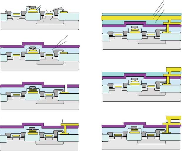
1. CMOS with W metallization
TiN/TiSi2 W poly Si PSG
n-Si n+ p well P+
2. LTO (SiO2) nad Si3N4 CVDSi3N4 (200 nm) LTO (300 nm)
5. PSG, poly Si, and PSG CVD
PSG (0.5 µm) poly Si (2 µm) PSG (1 µm)
3. Patterning, Si3N4, and LTO etching
4. Doped poly Si CVD poly Si (350 nm)
6. Rapid thermal annealing (1000°C, 1 min), patterning, PSG, and poly Si etching)
7. Sacrificial etching of PSG in buffered HF
Figure1.4 Fabricationprocessofsurface-micromachinedpolySimicrostructures integratedwithCMOScircuit.Source:BasedonYunetal.[2];Bustilloetal.[3].
thisreason,LSIfirstapproachiscommonlyusedasshowninFigure1.2.Thisis requirednottocontaminatetheLSIproductionlineaswell.
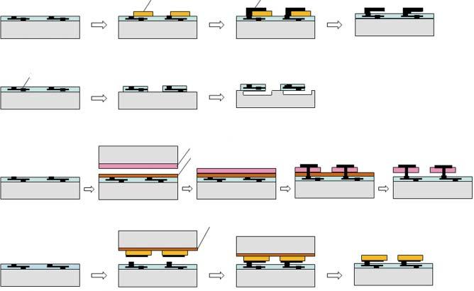
PolycrystallineSi(polySi)surfacemicromachiningusespolySiasthestructural layer.ThesurfacemicromachiningusingepitaxialpolySi(epi-polySi)willbe explainedinChapter3.ThepolySihasagoodmechanicalpropertyasamaterialfor spring,movingelement,etc.andcanbeusedforsensorsoractuatorsasresonators. Hightemperaturearound600 ∘ CisrequiredtodepositthepolySibychemicalvapor deposition(CVD).Theco-fabricatedIChastostandthistemperature.Resonant
Figure1.3
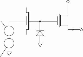
microstructuresmadeofpolySiwereintegratedwithdepletiontypeNMOSfield effecttransistor(FET)[4].ThefabricationprocessisshowninFigure1.3a[1,4].The NMOSFETsthathavepolySigatearefabricatedusingconventionallocaloxidation ofSi(LOCOS)technology.ThepolySilayerforthegateoftheFETisalsoused asadriveelectrodefortheresonator(1in(a)).Si3 N4 isdepositedandpatterned (etchedafterphotoresistpatterning)forthepurposeofetchstoplayerneededfor theetchingofthesacrificiallayer(2in(a)).Phosphosilicateglass(PSG)andSiO2 aredepositedbytheCVDforthepurposeofsacrificialspacerlayer(3in(a)).Poly Siisdepositedat600 ∘ Canddopedwithphosphorousbyionimplantation.Itis patternedafterrapidthermalannealing(RTA)at1150 ∘ Cforthreeminutes.The RTAisneededtocontrolthestressofthepolySi(4in(a)).Au(gold)isdepositedand patternedforbondingpads,andfinallythePSGsacrificiallayerisetchedoutinHF (hydrofluoricacid)tomakepolySimicrocantileverfortheresonator(5in(a)).The AuisusedonbehalfofconventionalAl(aluminum)becausetheAuisnotetched inHF.Photographsofthechipsurfaceandtheself-suspendedpolySicantilever fabricatedareshowninFigure1.3b.CircuitwiththeNMOSFETandtheresonator (resonantmicrobridge)areillustratedinFigure1.3c.Thecircuitforcapacitance detectionhastobemonolithicallyintegratedwiththeMEMSmicrostructurein ordertominimizetheinfluenceofstraycapacitance.
Thesurface-micromachinedpolySimicrostructureswereintegratedwithCMOS circuitaswell,beingcalledmodularintegrationofCMOSwithmicrostructures (MICS)[2,3].ThefabricationprocessisshowninFigure1.4.ThepolySisurface micromachiningrequires600 ∘ Cfordeposition,andthethermalbudgetrequires metallizationdifferentfromconventionalAl.W(tungsten)andTiN/TiSi2 wereused forthemetallizationanddiffusionbarrieratthemetal/siliconcontacts,respectively, tostandthehightemperatureprocess(1inthefigure).Low-temperatureoxide (LTO)(SiO2 )andSi3 N4 aredepositedbyCVD(2inthefigure),andtheSi3 N4 and theLTOarepatterned(3inthefigure).DopedpolySiisdepositedandpatterned (4inthefigure).PSG,polySi,and2nd PSGaredepositedbyCVD(5inthefigure). RTAismadeandthePSGandthepolySiarepatterned(6inthefigure).Movable polySimicrostructuresareformedbysacrificialetchingofthePSGinbufferedHF (7inthefigure).
ThethicknessofthepolySiislimitedtolessthan2 μmbecauseofitsstress,which causesabendingofthewafer.Ontheotherhand,low-stressepi-polySithatmakes alayerthicknessof20 μmormorepossiblewasdevelopedinFraunhoferInstitute forSiliconTechnologies(ISIT)inGermanyandUppsalaUniversityinSweden[5]. Surfacemicromachiningusingtheepi-polySihasbeenusedforcapacitivesensorsas accelerometerandgyroscope.Thelateralcapacitanceofmicromechanicalstructure canbeincreasedbecauseofthethickepi-polySilayer.Thecapacitancedetection circuitsneednottobemonolithicallyintegratedfortheSoCMEMS.Theepi-polySi surfacemicromachiningwillbeexplainedinChapter4.
ThepolySiGesurfacemicromachiningcategorizedinFigure1.1wasdevelopedto achievelowdepositiontemperature(410 ∘ C)[6].ThiswillbeexplainedinChapter5. Ge(germanium)isusedasthesacrificiallayerbecauseitcanbeetchedoutselectivelyinH2 O2 (hydrogenperoxide).
MetalsurfacemicromachiningwasdevelopedforthepurposeofmirrorarrayfabricatedonaCMOSLSI.Metalscanbedepositedbysputteringorevaporation.Since itdoesn’trequirehightemperature,thermaldamagetotheCMOSLSIisnotaproblemandphotoresistcanbeusedasasacrificiallayer.Thedurabilitywasimproved byusingamorphousmetal.Themirrorarrayhasbeenusedsuccessfullyforvideo projectorsandothersystemsaswillbeexplainedinChapter6.
TheothersurfacemicromachiningisaMEMSusingAlN(aluminumnitride).The AlNisapiezoelectricmaterialandcanbedepositedatlowtemperaturebyreactive sputtering.ThisenablesSoCMEMSthathavesurfacemicromachinedstructures havingpiezoelectricmaterialonacircuit.ThiswillbeexplainedinChapter7.
TheMEMSusingCMOSLSIwaferinFigure1.1istheSOCMEMSandschematicallyshowninFigure1.2b.ThemultilayersforinterconnectiononaCMOSwafer andthebulkSiareusedastheMEMSstructure,andtheSiundertheMEMSstructurecanbeunder-etchedifnecessary.ThiswillbeexplainedinChapter8.
WafertransfermethodsshowninFigure1.2cwillbeexplainedinChapter9.There aretwoways.Oneisfilmtransferinwhichstructurallayeronthecarrierwaferis transferredonanLSIwafer,andMEMSarefabricatedontheLSIwafer.Theotheris devicetransferinwhichMEMSarefabricatedonthecarrierwaferandtransferred ontheLSIwaferbyusingbumporothermethods.TheMEMSareleftontheLSI waferbyetchingoutthecarrierwaferorthetemporarybondinglayer,otherwise bydebonding(laserlift-off)theMEMSfromthecarrierwafer.Theadvantageofthe wafertransfermethodisthatthestructurallayerorMEMSarenotfabricatedonthe LSIwaferbutonthecarrierwafer,andhencethefabricationprocesshasflexibility. Hightemperatureprocesscanbeappliedonthecarrierwafer.
SomepiezoelectricmaterialsuchasPZT(leadzirconatetitanate)requireshigh temperature(700 ∘ C)fordepositionbysputtering.Thewafertransfermethodcanbe appliedforthefabricationoftheSoCMEMSwiththePZT.ThepiezoelectricMEMS willbedescribedinChapter10.
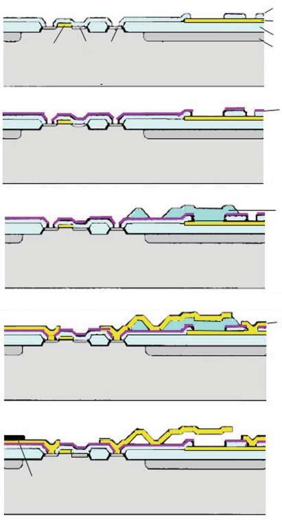
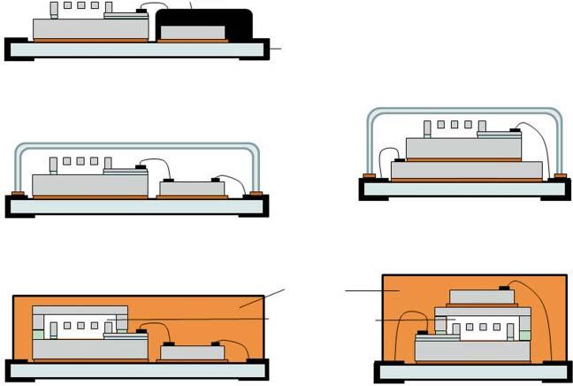
MonolithicSoCMEMShavebeendiscussedearlier.Theotherapproachisahybrid typecalledSiPMEMS.MEMSchipsandLSIchipscanbeconnectedwitheach otherasshowninFigure1.5.MEMSthathavetobeexposedasmicrophoneuse side-by-sideconfigurationwithLSIasshownininFigure1.5a.Theside-by-sideconfigurationofMEMSchipandLSIchip(Figure1.5b)andthestackedconfiguration ofMEMSchiponLSIchip(Figure1.5c)areplacedinacanorceramicpackage.The side-by-sideconfigurationofpackagedMEMSchipandLSIchip(Figure1.5d)and thestackedconfigurationofLSIchiponpackagedMEMSchip(Figure1.5e)canbe moldedwithpolymer.AnadvantageofthehybridapproachisthateachMEMSand LSIscanbefabricatedseparatelyusingoptimizedprocesses.
UnpackagedMEMSchipscan’tbemoldedwithresinbecausethesehavemoving elementsonthem.PackagingisneededforMEMSandespeciallyawaferlevelpackagingplaysimportantrolesinMEMS[7].Bonding,sealing,andinterconnection arerequiredfortheMEMSprocessandthepackaging.ThepackagedMEMSchip showninFigure1.5d,eusesglassfrit(solderglassandlow-melting-pointglass)for thebondingandsealing.ThiswillbeexplainedusingFigure4.6(Chapter4)and Figure17.35(Chapter17).SuchelementarytechnologiesfortheMEMSpackaging
Figure1.5 SiPMEMS(a)Side-by-sidehybridconfigurationofexposedMEMSchipand polymercoatedLSIchip,(b)Side-by-sidehybridconfigurationofMEMSchipandLSIchipin canorceramicpackage,(c)StackedhybridconfigurationofMEMSchiponLSIchipincanor ceramicpackage,(d)Side-bysidehybridconfigurationofpackagedMEMSchipandLSIchip withpolymermolding,(e)StackedconfigurationofLSIchiponpackagedMEMSchipwith polymermolding.
Figure1.6 Elementary technologiesforMEMS packaging. Bonding
Anodic bonding (Chapter 11)
Direct bonding (Chapter 12)
Metal bonding (Chapter 13)
Reactive bonding (Chapter 14)
Polymer bonding (Chapter 15)
Sealing and interconnection
Soldering by local heating (Chapter 16)
Packaging, sealing and interconnection (Chapter 17)
Vacuum packaging (Chapter 18)
Buried channel in monolithic Si (Chapter 19)
Through-substrate-vias (Chapter 20)
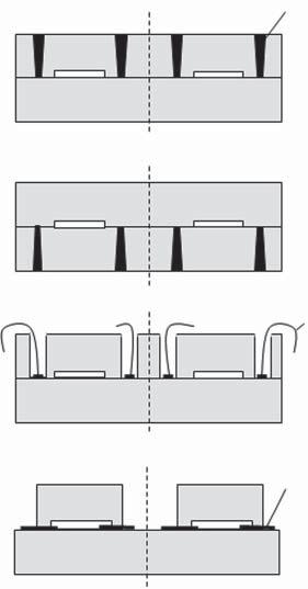
Figure1.7 Interconnectionmethods fromthepackagedMEMS (a)Through-substrate-vias(cap), (b)Through-substrate-vias (bottom),(c)Wire-bondedthrough-Si vias,(d)Lateralfeedthrough.
listedinFigure1.6willbeexplainedfromChapter11toChapter20ofthisbook.Five bondingmethodswillbeexplainedasfollows.Theseareanodicbonding(Chapter 10),directbonding(Chapter11),metalbonding(Chapter13),reactivebonding (Chapter14),andpolymerbonding(Chapter15).Sealingandinterconnection methodsexplainedaresolderingbylocalheating(Chapter16),packaging,sealing, andinterconnection(Chapter17),vacuumpackaging(Chapter18),buriedchannel inmonolithicSi(Chapter19),andthrough-substratevias(TSV)(Chapter20). InterconnectionmethodsfromthepackagedMEMSarecategorizedinFigure1.7. TheTSVinFigure1.7a,bwillbeexplainedinSection17.3.1andChapter20.The technologycalledwire-bondedthrough-Siviasin(c)willbeshowninSection 20.4.3.5[8].Thelateralfeedthroughinterconnectionin(d)willbediscussedin Section17.3.2.
References
1 Putty,M.W.,Chang,S.–C.,Howe,R.T.etal.(1989).Processintegrationforactive polysiliconresonantmicrostructures. Sens.Actuators 20:143–151.
2 Yun,W.,Howe,R.T.,andGray,P.R.(1992).Surfacemicromachined,digitally force-balancedaccelerometerwithintegratedCMOSdetectioncircuitry.IEEE Solid-StateSensorandActuatorWorkshop,HiltonHeadIsland,USA(22–15June 1992),126–131.
Bonding wire
3 Bustillo,J.M.,Fedder,G.K.,Nguyen,C.T.–C.,andHowe,R.T.(1994).Process technologyforthemodularintegrationofCMOSandpolysiliconmicrostructures. Microsyst.Technol. 1(1):30–41.
4 Howe,R.T.andMuller,R.S.(1984).Integratedresonant-microbridgevaporsensor. IEEEIEDM84,SanFrancisco,USA(9–12December1984),213–217.
5 Kirsten,M.,Wenk,B.,Ericson,F.,andSchweitz,J.A.(1995).Depositionofthick dopedpolysiliconfilmswithlowstressinanepitaxialreactorforsurfacemicromachiningapplications. ThinSolidFilms 259(2):181–187.
6 Takeuchi,H.,Quévy,E.,Bhave,S.A.etal.(2004).Ge-bladedamasceneprocessfor post-CMOSintegrationofnano-mechanicalresonators. IEEEElectronDeviceLett. 25(8):529–531.
7 Esashi,M.(2008).WaferlevelpackagingofMEMS. J.Micromech.Microeng. 18(7): 073001(13pp).
8 Fischer,A.C.,Grange,M.,Roxhed,N.etal.(2011).Wire-bondedthrough-silicon viaswithlowcapacitivesubstratecoupling. J.Micromech.Microeng. 21:085035 (8pp).
PartII
SystemonChip