https://ebookmass.com/product/2d-materials-fornanophotonics-young-min-jhon/
Instant digital products (PDF, ePub, MOBI) ready for you
Download now and discover formats that fit your needs...
Spintronic 2D Materials: Fundamentals and Applications (Materials Today) Wenqing Liu (Editor)
https://ebookmass.com/product/spintronic-2d-materials-fundamentalsand-applications-materials-today-wenqing-liu-editor/
ebookmass.com
Xenes 2D Synthetic Materials Beyond Graphene Alessandro Molle
https://ebookmass.com/product/xenes-2d-synthetic-materials-beyondgraphene-alessandro-molle/
ebookmass.com
Layered 2D Materials And Their Allied Application Inamuddin
https://ebookmass.com/product/layered-2d-materials-and-their-alliedapplication-inamuddin/
ebookmass.com
The Sins We Survive - A Reverse Harem Dark Romance: Love, Lust, and Liars Book #3 Danielle Renee
https://ebookmass.com/product/the-sins-we-survive-a-reverse-haremdark-romance-love-lust-and-liars-book-3-danielle-renee/
ebookmass.com
Partition of Unity Methods: The Extended Finite Element Method St¿Phane Bordas
https://ebookmass.com/product/partition-of-unity-methods-the-extendedfinite-element-method-stphane-bordas/
ebookmass.com
The Bible in History: How the Texts Have Shaped the Times 2nd Edition David W. Kling
https://ebookmass.com/product/the-bible-in-history-how-the-texts-haveshaped-the-times-2nd-edition-david-w-kling/
ebookmass.com
Empowerment Series: The Reluctant Welfare State 9th Edition – Ebook PDF Version
https://ebookmass.com/product/empowerment-series-the-reluctantwelfare-state-9th-edition-ebook-pdf-version/
ebookmass.com
Basic Immunology: Functions and Disorders of the Immune System 6th Edition Abul Abbas Mbbs
https://ebookmass.com/product/basic-immunology-functions-anddisorders-of-the-immune-system-6th-edition-abul-abbas-mbbs/
ebookmass.com
Peace and Conflict Studies Fourth Edition – Ebook PDF Version
https://ebookmass.com/product/peace-and-conflict-studies-fourthedition-ebook-pdf-version/
ebookmass.com
The Palgrave Handbook of Disabled Children’s Childhood Studies 1st Edition Katherine Runswick-Cole
https://ebookmass.com/product/the-palgrave-handbook-of-disabledchildrens-childhood-studies-1st-edition-katherine-runswick-cole/
ebookmass.com
2DMaterialsfor Nanophotonics Nanophotonics 2DMaterialsfor Nanophotonics Editedby
YoungMinJhon
SensorSystemResearchCenter, KoreaInstituteofScienceandTechnology,SouthKorea
JuHanLee
SchoolofElectricalandComputerEngineering, UniversityofSeoul,SouthKorea
SeriesEditor AkhleshLakhtakia
Elsevier
Radarweg29,POBox211,1000AEAmsterdam,Netherlands TheBoulevard,LangfordLane,Kidlington,OxfordOX51GB,UnitedKingdom 50HampshireStreet,5thFloor,Cambridge,MA02139,UnitedStates
Copyright©2021ElsevierLtd.Allrightsreserved.
Nopartofthispublicationmaybereproducedortransmittedinanyformorbyanymeans,electronic ormechanical,includingphotocopying,recording,oranyinformationstorageandretrievalsystem, withoutpermissioninwritingfromthepublisher.Detailsonhowtoseekpermission,further informationaboutthePublisher’spermissionspoliciesandourarrangementswithorganizationssuch astheCopyrightClearanceCenterandtheCopyrightLicensingAgency,canbefoundatourwebsite: www.elsevier.com/permissions.
Thisbookandtheindividualcontributionscontainedinitareprotectedundercopyrightbythe Publisher(otherthanasmaybenotedherein).
Notices
Knowledgeandbestpracticeinthisfieldareconstantlychanging.Asnewresearchandexperience broadenourunderstanding,changesinresearchmethods,professionalpractices,ormedical treatmentmaybecomenecessary.
Practitionersandresearchersmustalwaysrelyontheirownexperienceandknowledgeinevaluating andusinganyinformation,methods,compounds,orexperimentsdescribedherein.Inusingsuch informationormethodstheyshouldbemindfuloftheirownsafetyandthesafetyofothers,including partiesforwhomtheyhaveaprofessionalresponsibility.
Tothefullestextentofthelaw,neitherthePublishernortheauthors,contributors,oreditors,assume anyliabilityforanyinjuryand/ordamagetopersonsorpropertyasamatterofproductsliability, negligenceorotherwise,orfromanyuseoroperationofanymethods,products,instructions,orideas containedinthematerialherein.
BritishLibraryCataloguing-in-PublicationData
AcataloguerecordforthisbookisavailablefromtheBritishLibrary LibraryofCongressCataloging-in-PublicationData
AcatalogrecordforthisbookisavailablefromtheLibraryofCongress ISBN:978-0-12-818658-9
ForInformationonallElsevierpublications visitourwebsiteat https://www.elsevier.com/books-and-journals
Publisher: MatthewDeans
AcquisitionsEditor: SimonHolt
EditorialProjectManager: EmilyThomson
ProductionProjectManager: SojanP.Pazhayattil
CoverDesigner: VictoriaPearson
TypesetbyMPSLimited,Chennai,India
Listofcontributors...................................................................................................xi
CHAPTER1Synthesisofgrapheneandothertwo-dimensional materials ....................................................................... 1
NorbertoSalazar,CarlosMarquezandFranciscoGamiz
1.1 Introduction....................................................................................1
1.2 Synthesisofgraphene....................................................................3
1.2.1Top-downsynthesis............................................................3
1.2.2Bottom-upsynthesis............................................................8
1.2.3StructuralRamancharacterizationafterthesynthesis.....13
1.3 Synthesisofothertwo-dimensionalmaterials.............................14
1.3.1Micromechanicalexfoliation............................................16
1.3.2Ultrasonicexfoliation........................................................17
1.3.3Lithiumintercalatedandexfoliation................................18
1.3.4Hydro/solvothermalsynthesis...........................................19
1.3.5Templatesynthesis............................................................20
1.3.6Microwave-assistedmethod..............................................20
1.3.7Topochemicaltransformation...........................................23
1.3.8Pulsedlaserdeposition......................................................24
1.3.9Chemicalvapordeposition...............................................26
1.4 vanderWaalsheterostructures....................................................35
1.4.1Heterostructuresbymechanicalstacking.........................35
1.4.2Directsynthesisoftwo-dimensionalheterostructures.....41
1.5 Conclusion....................................................................................53 Acknowledgments.......................................................................53 References....................................................................................53
CHAPTER2Topologicalinsulatorsandapplications ................... 81
Chao-KueiLee,JuHanLee,Bai-TaoZhangand Jing-LiangHe
2.1 Introduction..................................................................................81
2.1.1Topologicalinsulators.......................................................81
2.2 Materialstructuresandpropertiesoftopologicalinsulators.......84
2.2.1Theoreticalapproachtotheelectronicandoptical propertiesoftopologicalinsulators..................................84
2.2.2Theopticalpropertyoftopologicalinsulators.................87 v
2.3 Applications..................................................................................97
2.3.1Topologicalinsulator basedSAfabrication methodsforlaserapplication............................................98
2.3.2Fiberizedsaturableabsorbersbasedon bulk-structuredBi2Te3 topologicalinsulators................101
2.3.3Pulsedsolid-statelasersbasedonbulk-structured topologicalinsulators......................................................121
2.4 Conclusion..................................................................................128 References..................................................................................128
CHAPTER3Blackphosphorus:deviceandapplication ............. 139 HongyanYang,YunzhenWang,Z.C.Tiu,LiboYuan andHanZhang
3.1 Introduction................................................................................139
3.2 Blackphosphorusproperties......................................................140
3.2.1Structureandnarrowbandgap........................................140
3.2.2Physicalproperty.............................................................142
3.3 Blackphosphorussynthesismethods.........................................147
3.3.1Typicaltop-downmethod...............................................147
3.3.2Thebottom-upmethod....................................................149
3.4 Nonlineareffectsoftwo-dimensionalmaterials........................151
3.5 All-opticaldeviceandapplication.............................................151
3.5.1Thephysicalmechanism.................................................151
3.5.2All-opticaldevicesandapplication................................153
3.6 Conclusionandperspective.......................................................158 Acknowledgments.....................................................................159 References..................................................................................159
4.1 Introduction................................................................................165
4.2 Ramanspectrumand2Dstructures...........................................168
4.2.1Bismuthtelluride,Bi2Te3 (topologicalinsulator)..........168
4.2.2Tungstentelluride,WTe2 (transition-metal dichalcogenide)...............................................................168
4.2.3Tinselenide,SnSe(transition-metal monochalcogenide).........................................................174
4.3 Electronicandopticalbandgap..................................................177
4.3.1Bismuthselenideandbismuthtelluride,Bi2Se3 andBi2Te3 (topologicalinsulator)..................................179
4.3.2Tungstentelluride,WTe2 (transition-metal dichalcogenide)...............................................................182
4.3.3Tinselenide,SnSe(transition-metal monochalcogenide).........................................................183
4.3.4Titaniumcarbo-nitrideTi3CN(metallicMXene)..........186
4.4 Saturableabsorptionandlasermodelocking............................187
4.4.1Bismuthselenideandbismuthtelluride,Bi2Te3 (topologicalinsulator).....................................................188
4.4.2Tungstentelluride,WTe2 (transition-metal dichalcogenide)...............................................................191
4.4.3Tinselenide,SnSe(transition-metal monochalcogenide).........................................................194
4.4.4Titaniumcarbo-nitrideTi3CN(metallicMXene)..........198
References..................................................................................202
CHAPTER5Signalprocessingbasedontwo-dimensional 5.1 Introduction................................................................................207
5.2 Quasiautocorrelationwithsaturableabsorption........................208
5.2.1Principle..........................................................................208
5.2.2Saturableabsorptionmaterialchoice andpreparation................................................................211
5.2.3Simulationandexperiments...........................................213
5.2.4Discussion.......................................................................218
5.3 All-opticaldeviceswiththermo-opticeffect.............................219
5.3.1Typicalstructuresofthermo-opticall-optical deviceswithlow-dimensionalmaterials........................220
5.3.2All-opticaldeviceswithMach Zehnder interferometer..................................................................221
5.3.3All-opticaldeviceswithMichelsoninterferometer........223
5.3.4All-opticaldeviceswithpolarizationinterferometer.....223
5.4 Futureprospects.........................................................................226
5.5 Conclusion..................................................................................227 Acknowledgment.......................................................................227 References..................................................................................227
CHAPTER6Terahertzphotonicapplicationsof two-dimensionalmaterials ....................................... 235 GeunchangChoi,Young-MiBahkandMinahSeo
6.1 Terahertztimedomainspectroscopy.........................................235
6.2 Terahertzphotonicapplicationsintwo-dimensional semiconductors...........................................................................236
6.2.1Terahertzapplicationsingraphene.................................236
6.2.2TerahertzapplicationsinMXene...................................240 References..................................................................................243
CHAPTER7Biosensorsbasedontwo-dimensionalmaterials .... 245 MarcoFilice,JuanA.MarchalandFranciscoGamiz
7.1 Introduction................................................................................245
7.2 Bioreceptorsfortwo-dimensional-basednano-biosensors........248
7.2.1Antigen antibodybioreceptors......................................248
7.2.2Deoxyribonucleicacidbioreceptors...............................249
7.2.3Enzymecatalyticbioreceptors........................................250
7.3 Two-dimensionalnanomaterialsastransductors:sensing mechanisms................................................................................250
7.3.1Two-dimensionalbiosensorsbasedonoptical detectionmethods...........................................................250
7.3.2Biosensorsbasedonfield-effecttransistors...................255
7.3.3Biosensorsbasedonelectrochemicalmethods..............266
7.4 Surfacefunctionalizationstrategiesfortwo-dimensional materials.....................................................................................272
7.4.1Covalentfunctionalizationstrategies..............................273
7.4.2Noncovalentfunctionalizationstrategies........................279
7.4.3Nongraphenetwo-dimensionalmaterials functionalization..............................................................283
7.5 Clinical/preclinicalapplicationsoftwo-dimensional material basedbiosensors.........................................................285
7.5.1Applicationsoftwo-dimensionalmaterial based biosensors:generaloverview..........................................286
7.5.2Applicationsoftwo-dimensionalmaterial based biosensors:cancerbiomarkerdetection..........................288 Acknowledgments.....................................................................291 References..................................................................................292
CHAPTER8Computationalsimulationsof2Dmaterials ............. 313
YoungInJhonandYoungMinJhon
8.1 Chargeandthermaltransportin2Dmaterials..........................313
8.1.1Chargetransport:deformationpotential.........................314
8.1.2Thermalconductivity:phononBoltzmanntransport equation...........................................................................317
8.1.3Casestudiesforapplication............................................318
8.2 LatticevibrationsandRamanspectraof2Dmaterials.............321
8.2.1LatticevibrationalmodesandRamanscattering...........324
8.2.2Casestudiesforapplication............................................327
8.3 Opticalandexcitonicpropertiesof2Dmaterials......................334
8.3.1Kubo Greenwoodformulationforlinearoptical responses.........................................................................335
8.3.2Bethe Salpeterequationforexcitonicboundstates.....336
8.3.3Casestudiesforapplication............................................337 References..................................................................................341
9.1 Overview....................................................................................347
9.2 Nonlinearopticalphenomenaandtechniquesused..................347
9.3 Graphene.....................................................................................350
9.4 Topologicalinsulators................................................................359
9.5 Blackphosphorus.......................................................................362
9.6 Transitionmetaldichalcogenides..............................................365
9.7 Hexagonalboronnitride.............................................................370
Listofcontributors Young-MiBahk
DepartmentofPhysics,IncheonNationalUniversity,Incheon,Republicof Korea
GeunchangChoi
DepartmentofPhysics,UniversityofOttawa,Ottawa,ON,Canada
MarcoFilice
NanobiotechnologyforLifeSciencesGroup,DepartmentofChemistryin PharmaceuticalSciences,FacultyofPharmacy,UniversidadComplutensede Madrid(UCM),Madrid,Spain;MicroscopyandDynamicImagingUnit, Fundacio ´ nCentroNacionaldeInvestigacionesCardiovascularesCarlosIII (F.S.P.CNIC),Madrid,Spain
FranciscoGamiz
BiosanitaryResearchinstituteibs.Granada,UniversityofGranada,Granada, Spain;ResearchUnit“ModelingNature”(MNat),UniversityofGranada, Granada,Spain;LaboratoryofNanoelectronics,Grapheneand Two-dimensionalMaterials,DepartmentofElectronicsandComputerScience, CITIC-UGR,UniversityofGranada,Granada,Spain
Jing-LiangHe
StateofKeyLaboratoryofCrystalMaterials,ShandongUniversity,Jinan, PeopleRepublicofChina
YoungIn-Jhon
SchoolofElectricalandComputerEngineering,UniversityofSeoul,Seoul, RepublicofKorea;DepartmentofElectricalandComputerEngineering (BrainKorea21Plus),UniversityofSeoul,Seoul,RepublicofKorea
YoungMinJhon
SensorSystemResearchCenter,KoreaInstituteofSciecneandTechnology, Seoul,Korea
IvanM.Kislyakov
LaboratoryofMicro-NanoOptoelectronicMaterialsandDevices,Key LaboratoryofMaterialsforHigh-PowerLaser,ShanghaiInstituteofOpticsand FineMechanics,ChineseAcademyofSciences,Shanghai,P.R.China
Chao-KueiLee
DepartmentofPhotonics,NationalSunYat-senUniversity,Taiwan,Republicof China
JuHanLee
SchoolofElectricalandComputerEngineering,FacultyofEngineering, UniversityofSeoul,Seoul,RepublicofKorea
GuoqingMa
LaboratoryofMicro-NanoOptoelectronicMaterialsandDevices,Key LaboratoryofMaterialsforHigh-PowerLaser,ShanghaiInstituteofOpticsand FineMechanics,ChineseAcademyofSciences,Shanghai,P.R.China
JuanA.Marchal
DepartmentofHumanAnatomyandEmbryology,FacultyofMedicine, UniversityofGranada,Granada,Spain;BiopathologyandRegenerative MedicineInstitute(IBIMER),CentreforBiomedicalResearch,Universityof Granada,Granada,Spain;BiosanitaryResearchinstituteibs.Granada, UniversityofGranada,Granada,Spain;ResearchUnit“ModelingNature” (MNat),UniversityofGranada,Granada,Spain
CarlosMarquez
InstitutodeInvestigacio ´ nBiosanitaria,ibs.Granada,Granada,Spain
YoungMin-Jhon
SensorSystemResearchCenter,KoreaInstituteofScienceandTechnology, Seoul,RepublicofKorea
NorbertoSalazar
LaboratoryofNanoelectronics,Grapheneand2DMaterials,ResearchCenter forInformationandCommunicationsTechnologies,CITIC-UGR,Universityof Granada,Granada,Spain
MinahSeo
SensorSystemResearchCenter,KoreaInstituteofScienceandTechnology (KIST),Seoul,RepublicofKorea
Z.C.Tiu
CollegeofOptoelectronicEngineering,ShenzhenUniversity,Shenzhen,P.R. China;Facultyofengineering,SEGiCollegeSubangJaya,Selangor,Malaysia
JunWang
LaboratoryofMicro-NanoOptoelectronicMaterialsandDevices,Key LaboratoryofMaterialsforHigh-PowerLaser,ShanghaiInstituteofOpticsand FineMechanics,ChineseAcademyofSciences,Shanghai,P.R.China
YunzhenWang
CollegeofOptoelectronicEngineering,ShenzhenUniversity,Shenzhen,P.R. China;InternationalCollaborativeLaboratoryof2DMaterialsfor OptoelectronicsScienceandTechnologyofMinistryofEducation,Shenzhen University,Shenzhen,P.R.China
KanWu
StateKeyLaboratoryofAdvancedOpticalCommunicationSystemsand Networks,DepartmentofElectronicEngineering,ShanghaiJiaoTong University,Shanghai,P.R.China
HongyanYang
CollegeofOptoelectronicEngineering,ShenzhenUniversity,Shenzhen,P.R. China;GuangxiKeyLaboratoryofAutomaticDetectingTechnologyand Instruments,GuilinUniversityofElectronicTechnology,Guilin,P.R.China; GuangxiKeyLaboratoryofOptoelectronicInformationProcessing,Guilin UniversityofElectronicTechnology,Guilin,P.R.China
LiboYuan
GuangxiKeyLaboratoryofOptoelectronicInformationProcessing,Guilin UniversityofElectronicTechnology,Guilin,P.R.China;GuangxiKeyLaboratory ofAutomaticDetectingTechnologyandInstruments,GuilinUniversityof ElectronicTechnology,Guilin,P.R.China
Bai-TaoZhang
StateofKeyLaboratoryofCrystalMaterials,ShandongUniversity,Jinan, PeopleRepublicofChina
HanZhang
CollegeofOptoelectronicEngineering,ShenzhenUniversity,Shenzhen,P.R. China;InternationalCollaborativeLaboratoryof2DMaterialsfor OptoelectronicsScienceandTechnologyofMinistryofEducation,Shenzhen University,Shenzhen,P.R.China
Synthesisofgrapheneand othertwo-dimensional materials 1 NorbertoSalazar1,CarlosMarquez2 andFranciscoGamiz3
1LaboratoryofNanoelectronics,Grapheneand2DMaterials,ResearchCenterforInformation andCommunicationsTechnologies,CITIC-UGR,UniversityofGranada,Granada,Spain
2InstitutodeInvestigacio´nBiosanitaria,ibs.Granada,Granada,Spain
3ResearchUnit“ModelingNature”(MNat),UniversityofGranada,Granada,Spain
1.1 Introduction Whenanelectricfieldisappliedacrossathree-dimensional(3D)crystallinesolid, theelectronsrespondbymovingwithanaveragevelocity(driftvelocity).Thisvelocityislimitedbythescatteringwithcrystaldefects,phonons,impurities,grainboundaries,etc.However,intwo-dimensional(2D)materials,theinfluenceofthe scatteringmechanismbydefectsonthematerialresistanceisreduced,andballistic transportatdistancesupto1 μmhasbeendemonstratedingraphene [1].Thusinan ideal2Dmaterial,electronscanmovewithaverylowscatteringprobability.This factmightmeansignificantimprovementsintermsofelectricalparameters(mobility, conductivity,etc.)comparedtostandard3Dlattices.Moreover,2Dmaterialsexhibit otherpromisingpropertiesinterestingforphotonicapplications:theirsurfacesarenaturallypassivatedwithoutanydanglingbonds,facilitatingtheintegrationof2Dmaterialswithphotonicstructuressuchaswaveguidesandcavities [2].Aswewill describeafterward,itisalsopossibletoconstructverticalheterostructuresusingdifferent2Dmaterialswithouttheconventional“latticemismatch”issueof3Dsolids, sincelayerswithdifferentlatticeconstantsinheterostructuresareonlyweakly bondedbyvanderWaals(vdW)forcesasin layeredbulkmaterials.Infact,despite beingatomicallythin,many2Dmaterialsinteractwithlightstrongly.Forexample,a singlelayerofmolybdenumdisulfide(MoS2)absorbsaround10%oflightatexcitonicresonances(615and660nm) [2].Orgraphene,asingleatomiclayerofgraphite,theisolationofwhichwasawardedaNobelPrizein2010,theoreticallycan reachelectricalmobilitiesupto200,000cm2/Vs,Young’smodulusof1TPaand intrinsicstrengthof130GPa,highthermalconductivity(above3000W/mK),and opticalabsorptionof πα 2.3%(intheinfraredlimit,where α isthefinestructure constant) [3 5].Inthiscontext,transparency,conductivity,andelasticitycanbe usedinflexibleelectronics,whereastransparency,impermeability,andconductivity willfindapplicationinprotectivecoatingsandbarrierfilms,besidesthedirect
2DMaterialsforNanophotonics.DOI: https://doi.org/10.1016/B978-0-12-818658-9.00006-5 © 2021ElsevierLtd.Allrightsreserved.
electronicandphotonicapplications.However,twoissuesarestillongoingnowadays: (1)graphenepresentsazero-overlapsemimetalcharacteristic,whichunfortunately limitsitsuseindigitalelectronics,where highratiobetweenthecurrentinthe“on” and“off”statesandlowpowerconsumptionin“off”statearerequiredaswellas preventstherealizationofefficientlight-emittingdevicesand(2)thefabricationof large-scaleandreliablestructuresisstillacomplicatedandnotwell-resolvedtask.As alternativeorcomplementtoresolvetheselimitations,transitionmetaldichalcogenides(TMDs),2DlayeredmaterialswiththeformulaMX2,whereMisatransition metal(Mo,W,Hf,etc.)andXisachalcogen(Se,Te,S),haveexperiencedahuge growthofinterestintherecentyears.Asingraphene,thereducedthicknessprovides optimalelectrostaticcontrolproviding these2Dmaterialsbetterimmunitytoshortchanneleffectsthantheplanarsiliconcounterparts [6].Interestingly,anindirectto directbandgaptransitionoccursasthefilmthicknessoftheseTMDmaterialsis reducedfrommultilayertomonolayerduetoquantumconfinement.Infact,they exhibitopticalbandgapsintherangeof1 2eV,makingthemsuitablefornearinfraredabsorptionandemissionwithstrongphotoluminescence.Complementarily, thebandgapsinTMDshavealsobeenshowntobetunable,overarangefromsemiconductingtonearmetallic,viatheapplicationofexternalelectricfieldsaswellas mechanicalstrain [2].Someadditionalelectricalpropertiespredictedforthese2D materialsaremobilitiesfrom200to400cm2/Vs [7,8],veryhigh“on”/“off”ratios largerthan1010,andalargetransconductanceof4.4mS/μm [8],current-carrying capabilitiesofabout5 3 107 A/cm2 [9] andsubthresholdswingofabout60mV/ decade [7].Accordingtotheguidelinesforlow operatingpowertechnologies, InternationalRoadmapforDevicesandSystems(IRDS),initsBeyondCMOSedition [10],TMDdevicespresentadvantagesintermsofhigher“on”/“off”ratios, muchlowerpowerconsumptionandcurrent leakage,andgoodswitchingdelaycomparingwithsilicondevices.
Evensolvingthezero-bandgapissuedemonstratedingrapheneanddespitethe theoreticallypromisingpropertiesofthese2Dmaterials,fabricateddevicesrarely fitwiththeexpectedresults.Thefabricationprocessisstillabottleneckinterms ofpossibleapplications,bothingrapheneandinTMDdevices.Forexample,the veryfirstfew-layerMoS2 FETswithSiO2 asgatedielectricfabricatedby Novoselovetal. [4] demonstratedverypoorpropertiessuchasmobilitiesinthe rangeof0.53cm2/(Vs).Inordertoimprovethisfigureofmerit,dielectricengineeringhasbeenproposedtosuppressCoulombscatteringinTMDschannels increasingtheperformance [11,12].Unfortunately,aswellasinothertechnologies(siliconandIII Vcompounds),introducingnewgatematerialsincreasesthe devicecomplexityresultingintheappearanceofdefectstates(oxidetraps,interfacestates,defectinthesemiconductorchannel,andamongothers.)thatdegrade thedeviceperformanceandreliability.Besidesthisissue,itisnotedthatthe majorityofreporteddeviceresultsareobtainedfromexfoliatedandtransferred 2Ddevices,wherethescalabilityinthefabricationprocessisstillachallengeto overcome.Regardingthesamplesgrownbychemicalvapordeposition(CVD), thetransportpropertiesareinferior [13].However,thefactorslimitingthe
electricalandopticalpropertiesof2Dmaterialsanddevicesarestillnotwell understood.Studiesonmultilayer2Dmaterialsandinsightsintotheinteractions betweenthelayersareatanearlystage.Inaddition,somemechanismsdegrading theperformanceofthedevicedependonthesynthesismethod,substrate,gate oxidematerial,andoxide metalstructure,increasingthecomplexitytoaddress systematicstudies.Ingeneral,grainboundaries,corrugations,vacancies,trapsand mobilechargeshavedemonstratedperformancedeterioration.Theimportanceof thesedegradingmechanismsdependsonthesynthesismethod.Thereforethefabricationprocessplaysanimportantroleinthefinalpropertiesofthedevicesdemonstratingthatchoosingtheappropriatesynthesismethodiscriticalforthe realizationofphotonicsandelectronicdevices.Aspossibilities,therearehighqualitymethodssuchasmechanicalexfoliation [1] orCVDmethodswithoutstandingresultsintermsofelectrical,mechanical,optical,andthermalproperties butwithahighcostandpoorscalability,andalso,othermethodssuchaschemicalexfoliationwithworseproperties,butmoreaffordableandscalableand,therefore,moresuitableforsomelarge-scaleindustrialapplications.Infact,the solutiontoproblemssuchasthelimitedgraphenemassproductionandpoor reproducibilityofdeviceperformanceisveryimportantinordertopushthe2D materialstechnologyintothemarket.Inthischapter,wedescribethemainsynthesismethodsinthefabricationofgraphene,promising2Dmaterialssuchas TMDs,blackphosphorous,hexagonalboronnitride(h-BN),andfinally,especial attentionwillbedevotedtotherecentadvancesintheassemblyof2D heterostructures.
1.2 Synthesisofgraphene Asmentioned,duetotheoutstandingproperties,severaltechniquestosynthesize graphenehavebeeninvestigated,beingclassifiedintwomainapproaches;topdownandbottom-up, Fig.1.1.Thefirstapproach,top-down,involvestheproductionofgraphenestartingfrombulkgraphite,whereasinbottom-upsynthesisgrapheneisgrownfromcarbonsourcesonvarioussubstratesthataresubsequently removedlatterly.Thefirstmethodsreportedwerethemechanicalexfoliation, obtainedforthefirsttimebyNovoselov’sgroup [1,4],andtheepitaxialgraphene growthonsiliconcarbide(SiC)developedbydeHeer’sgroup [14,15].These lattermethodstogetherwiththechemicalandthermalexfoliation [16 18] andCVD [19] areconsideredthemostusedtechniquesforthesynthesisof thegraphene.
1.2.1 Top-downsynthesis Top-downsynthesisapproachinvolvestheproductionofgraphenestartingfrom bulkgraphite,usuallythroughaprocessofexfoliation.Graphenemechanical
FIGURE1.1
Summaryofthegraphenesynthesistechniques.
FIGURE1.2
Micromechanicallyexfoliatedgraphene.Opticalimagesof(A)thingraphiteand(B)FLG andsingle-layergraphene(lighterpurplecontrast)ona B300nmSiO2 layer.Yellow-like colorindicatesthickersamples(B100sofnm)whilebluishandlightercontrastindicates thinnersamples. FLG,Few-layergraphene.
ReprintedfromC.Soldano,A.Mahmood,E.Dujardin,Production,propertiesandpotentialofgrapheme, Carbon48(2010)2127 2150 [20], ©2010withpermissionfromElsevier.
exfoliation,introducedinRef. [1] consistsoftherepeatedpeelingofsmallmesas ofhighlyorientedpyrolyticgraphite(HOPG).Thetapecontainingopticallytransparentflakesisthendissolvedinacetone;afewstepslatertheflakescontaining bothmultilayerandmonolayergraphenearetransferredtoatargetwafertobe characterized.Thistechniquehasbeenlatermodifiedremovingtheliquidstage.
Fig.1.2 showsopticalmicroscopeimagesofmicromechanicalexfoliatedgraphenewheredifferentflakethicknessesaredistinguished.Exfoliatedgraphene
behaveslikeazero-bandgapsemiconductororasmall-overlapsemimetal,in whichbothpositiveandnegativegatevoltagesinduce2Delectronsandholes, respectively,inconcentrationsupto1013 cm 2 anddemonstratedmobilityvalues between2000and5000cm2/Vs [4].Theeasinessofthesynthesistechniqueand thesurprisingqualityofthegrapheneobtainedhaveallowedthatmicromechanicalexfoliationcanbeusedtogeneratehigh-qualitygraphenethatiselectrically isolatedforfundamentalstudiesoftransportphysicsandotherpropertiesbutdoes notyetappeartobescalabletolargearea.
Morescalablemethods,insidethetop-downapproach,requireachemical exfoliationprocesstoobtaingrapheneoxide(GO).Ingeneral,GOissynthesized byeithertheBrodie [21],Staudenmaier [22],orHummersandOffeman [23] methods.Allthethreemethodsinvolveoxidationofgraphitetovariouslevels. BrodieandStaudenmaierusedacombinationofpotassiumchlorate(KClO3)with nitricacid(HNO3)tooxidizegraphite,andtheHummersmethodinvolvesthe treatmentofgraphitewithpotassiumpermanganate(KMnO4)andsulfuricacid (H2SO4).Hummer’sapproachissummarizedin Fig.1.3.Theprocessisdivided intothreesequentialphasesatdifferenttemperatures,illustratedwithdifferent colors.Duringthefirststep,oxidizingagents,sulfuricacid,nitricacid,andpotassiumpermanganatearemixed.Thereactionoxidizesthegraphite,introduces functionalgroups,andincreasestheinterlayerdistancebetweengraphitelayers, decreasingthevdWforcesandfacilitatingthegrapheneexfoliation(schematic
FIGURE1.3
SchematicdescriptionofthegraphiteoxidationtoobtainGObasedonHummer’smethod.
viewintherightpartof Fig.1.3).Next,waterandhydrogenperoxidesareadded athightemperatures.Theresultingsolutioncontainsanimportantquantityof acid,aswellasmetallicionsandinorganicimpurities.Thereforeitisthenpoured severaltimestodecreasethecontentofacid.Thelastpartoftheoxidationprocessinvolvesafilteringwithhydrochloricacid.Theobtainedgrapheneoxide behavesasanelectricalinsulatorduetothealterationsufferedbythecarbon atomsduringtheoxidationprocess(GOhassp2 andsp3 hybridizedcarbon atoms).
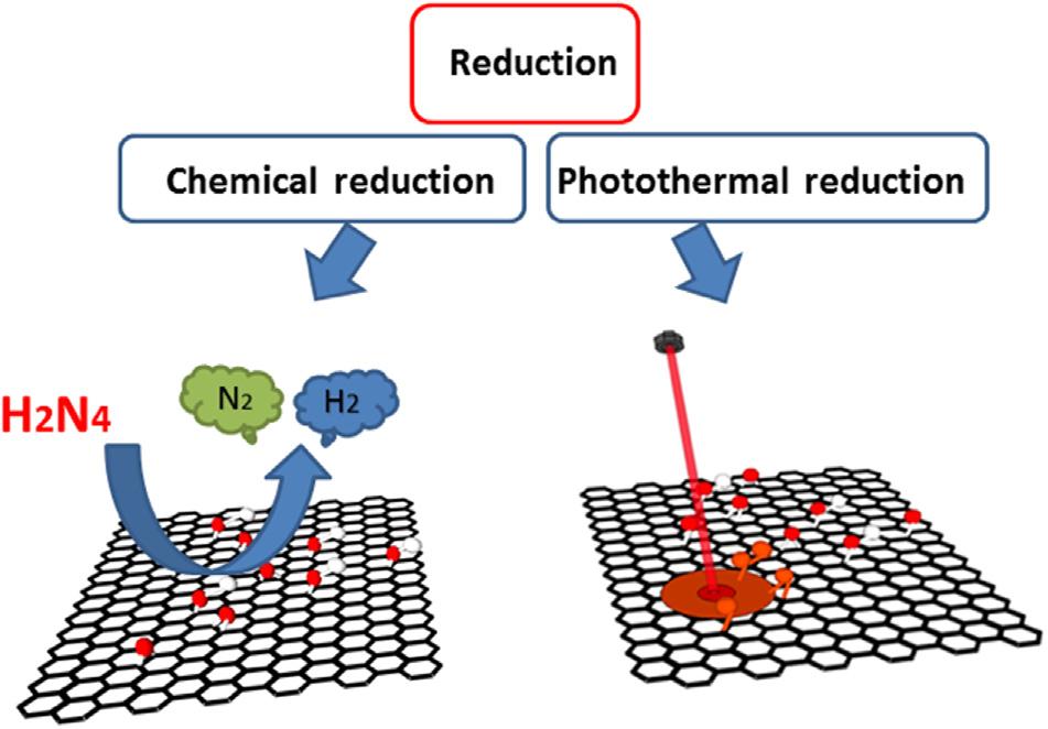
Despitethealterationsufferedinthegrapheneoxidestructureduringthe chemicaloxidation,thesemimetalbehaviorcanberecoveredbyremovingthe functionalgroupsand,thus,partiallyrestoringtheoriginalsp2 electronicstructure.Theexfoliationprocesscanbecompletedbychemicalmethods[using reductionagentsashydrazine(N2H4)] [18,24,25] orthroughthermaltreatments [25],asobservedin Fig.1.4.Thechemicalreductionimpliestheuseofcorrosive, flammable,andtoxicagents.Besides,thiskindofreductionmayintroduceimpurities.Analternativeistheuseofthermalannealing.Inthisapproachthereductionofthegrapheneoxidecanbedirectlyachievedheatingonahotplate [26], infraredheatlamp [27],annealinginafurnace [17] ordirectlyexposingthefilm tothephotothermalenergyofalaserbeamtogeneratelocalizedhightemperatures [28].ThehightemperaturesbreaktheC OandC 5 Oboundsofthecarbon sheets,whileCatomsarereorganizedbythefastexpansionofthesheetsduring deoxygenation.
FIGURE1.4
Schematicillustrationofthepossiblereductionmethodsofgrapheneoxideaccordingto theLerf Klinowskimodel [29].Left,usingareductionmethodwherechemicalsare employedtoremovethefunctionalgroups.Right,thesemimetalbehaviorisrecovered thankstothephotothermalenergyofalaserbeam.
AsdemonstrateinRefs. [30,31],theuseofalaserisextremelyattractive allowingtodesignprecisely(conductive)reducedgrapheneoxide(rGO)patterns surroundedby(insulator)GO.Ascomparedwithotherlithographictechniques, thelaser-scribingtechnologyissimple,low-cost,scalable,veryfast,andfully compatiblewithflexiblesubstrates.However,thistechniquepresentspractical limitationsforthepossibleuseinphotonicapplications:despitesomeworksthat haveachievedlarge-scaleandsingle-layerreducedgrapheneoxidefilms [32],it isstilldifficulttocontrolthefilmthicknessandtransparencyforhigh-standard electricalproperties.Infact,afterthereductionprocess,therGOpresentsametallicblackcolor,whereasthenonreducedgrapheneoxideareasremaininasemitransparenttone.Abalancebetweenelectricalpropertiesandtransparencycanbe struckmodifyingthegrapheneoxideconcentrationandthelaserpower(powerof thereduction)orreducingtheconcentration(dilutingthegrapheneoxide).
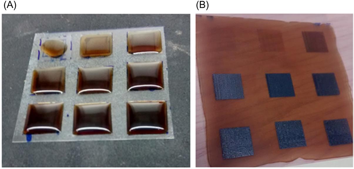
Fig.1.5 showsanexampleofmultilayerreducedgrapheneoxidesamplesona flexibleplasticsubstratewheresquaresstructuresaredepositedwithadifferent grapheneoxideconcentration(Fig.1.5A)orreducedatincreasinglaserpower intensities(Fig.1.5B).Thetransparencyclearlydecreasedasafunctionofthe concentrationandthereductionpower,whileelectricalpropertiesaredocumented toincrease [30].
Despitethefunctionalgroupsingrapheneoxidecanberemovedthrough chemicalorthermalreduction,largedefectdensitiescanremaininthelayer,disruptingtheelectronicsproperties [18].Thereforetocoverthelarge-arearequirementstogetherwithhigh-qualitygraphene,othersolutionshavebeenproposed. Oneofthemistheliquidexfoliationofgraphitetodirectlyobtaingrapheneflakes [33 35],alsocalledsolventsonicationorsurfactant-mediatedexfoliation.The
Examplesofgrapheneoxidesamples.(A)MultilayerGOdepositedonPETwithincreasing volume,from45to405 μLofa4mg/mLsolution.(B)GOfora4mg/mLconcentration reducedatincreasinglaserpowerintensities,from65to105mWatawavelengthof 550nm. PET,Plasticflexiblesubstrate.
FIGURE1.5
ultrasoundofgraphiteinsolventsresultsintheexfoliationandcuttingofthe graphitecrystallitestogivegraphenenanosheets.Thesesheetsarethenstabilized, eitherbyinteractionwiththesolventorbythepresenceofadsorbedsurfactantor polymer.Dependingonthesonicationtimeandthesolvent,avarietyofflake thicknessesandsizesareobtained.Apracticalproblemofthismethod,in-depth documentedinRef. [33],isthattodispersegrapheneathighconcentrations,the solventshavethecorrectsurfaceenergyandalsohavehighboilingpoints,makingdifficultthelaterevaporation.Otherwise,solventssuchasisopropanoland acetone,withrelativelylowboilingpoints,dispersegrapheneatconcentrations muchlowerthanthebettersolvents.Thusfurtherworktoscaleupthesolvent exfoliationisrequired.Moreover,studiesofliquid-phaseexfoliation(LPE)of pristinegraphitehavebeencarriedoutbyultrasonicationinstabilizingsolvents [36],inthepresenceofdifferentsurfactants [37,38],polymers [39],orevenmetal atoms [39,40],whichrepresentalternativewaystoproducehigh-qualitygraphene flakes.Anotheralternativeforthedirectgrapheneexfoliationwasproposedin Ref. [41] andcarriedoutbyusinganintensecavitationfieldinapressurized ultrasonicreactor.Themethodsappliedanonoxidativetreatmentonnatural graphiteundertheactionofanintensecavitationfieldinapressurizedflowor batchultrasoundreactor.Accordingtothiswork [41],thebenefitsofdelaminationbyusinghigh-powerultrasoundinapressurizedreactor,comparedtodelaminationthroughsonication,are(1)itallowsthepreparationofgraphenewith differentparticlemorphologies(flat,not-deformedplate)and(2)itallowsthe preparationoftensofgramsofgrapheneperhour.However,theneedofaspecificreactorequipmentcanincreasethesynthesiscost.
1.2.2 Bottom-upsynthesis Thebottom-upsynthesisapproachconsistsofthegraphenegrowthonvarious substratesthataresubsequentlyremoved.Thesetechniquespursuethefabrication oflarge-scalegraphenewhilesustaininghighstandardsintermsofelectrical,photonic,andmechanicalproperties.Themostimportantaretheepitaxialandthe CVDgrowths.Theepitaxialgrowthconsistsofthesublimationofafewatomic layersofSifromamonocrystallineSiCsubstrate [14,42].Beingbothpolarsurfaces,theSi-terminated(0001)andtheC-terminated(000 1)intheSiC wafer,annealingathigh-temperatureunderultrahighvacuum(UHV),tendto graphitizethem,becauseofSievaporation [5].However,theypresentsignificant differencesinthethicknessesofthegrapheneformedlayers.Graphenelayersare rapidlyformedonthecarbonfacesresultinginthickfilmswith5 100layers, whereasarelativelyslowformationtakesplaceonthesiliconfaceresultingin theformationofverythinsamples [43].OntheC-face,largerdomains (B200nm)ofmultilayered,rotationallydisorderedgrapheneareproduced.On theSi-face,UHVannealingleadstosmalldomains, B30 100nm [44].The mostusualprocessinvolvesthegraphenegrownontheC-faceofa3C-,4H-,or 6H-SiCsubstrate.Sublimationiscommonlydoneinaradiofrequencyinduction
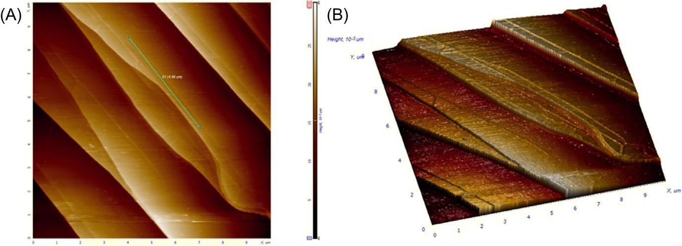
furnaceattemperaturesrangingfrom1450 Cto1550 C.Theprocessingtimein thesecasesisabout5min [42]. Fig.1.6 showstheatomicforcemicroscopy imageofgraphenegrownontheSi-faceofaSiCwafer.
However,thegrowthoflayersbysiliconsublimationinUHVtypicallyresults inlessqualityfilmsthanexpectedpresentingsomedefectsinthestructure.To solvethisissue,alternativegraphitizationmethodshavebeenrecentlydeveloped: Emtsevetal. [45] proposedtheuseofargoninafurnaceatnearambientpressure (1bar)toreducetheSisublimationratereachingmobilitiesupto930cm2/Vsat roomtemperature.Ontheotherhand,deHeeretal.proposedtheconfinementcontrolledsublimationmethod [43].Inthismethodthereactioniscarriedout eitherinvacuumorinaninertgas,limitingtheSiescapeandthusmaintaininga highSivaporpressuretoachievequasiequilibriumconditions.Single-andfewlayergraphenefilmscanbeproducedoverlarge(cmscale)areas,bothonSi-and C-faces.Intheseworks,graphenegrownontheSi-facehasamobilityatroom temperatureof B500 2000cm2/Vs,withvaluesontheC-faceabout B10,000 30,000cm2/Vs [43,44,46].Regardingelectronicsorphotonicsapplication,single-gatedgraphenetransistorswithhigh-kdielectrichavebeendemonstratedonmultilayergraphenewithmobilitiesupto5000cm2/Vs,and Ion/Ioff ratiosofuptosevenemployingtheepitaxialgrowthonSiCwafers [47]. However,thelimitationsofthistechnologyarerelatedtotheSiCwaferscost (between$160and$290for2-in.waferat2019prices,comparedtoabout$5 $10forsamesizeSiwafers)andtheirsmallersize(usuallynolargerthan6in.) comparedtoSiwafers.Infact,siliconwasconsideredasapossiblesubstratefor graphenelayerepitaxialgrowthespeciallybecauseofitsavailabilityintheform oflarge-scalewafers.However,therelativelyhighcarbonsolubilitytogetherwith
FIGURE1.6
Atomicforcemicroscopy(AFM)topographyimageofepitaxialgrowngrapheneona6HSiC(0001)substrate:(A)in2Dand(B)in3Drepresentation.Thestructureis characterizedbyaseriesofterraces.Itisimportanttonotethatthesurfaceheight variationshownisnotthegraphenethicknessvariationbutthetotalsurfaceroughness, whichincludesthemultilayeredgraphenethicknessandsignificantroughnessintheSiC underneath. 2D,Two-dimensional; 3D,three-dimensional.
therelativelylowcarbondiffusivityonthesiliconsurfacelimitstheuseofSi wafersforthispurpose [48,49].Complementarily,someworkshavedemonstrated methodstotransfergraphenegrownonSiCtoanothersubstrateviaexfoliation, particularlywithaNifilm [50].Despitethemobilities,calculatedfromthemaximumtransconductance,reportabout1700 2500cm2/Vs,two-stepexfoliation processisrequiredlimitingtheindustrialscale.
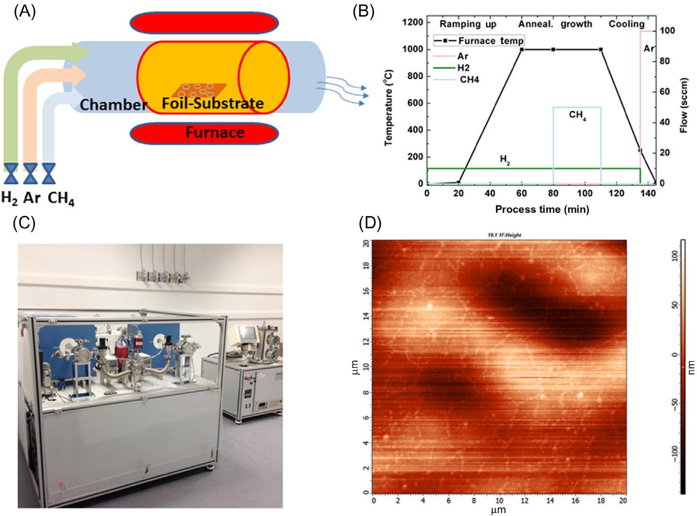
TogetherwithepitaxialgrowthonSiCwafers,CVDisthemostimportant bottom-upsynthesisapproach.CVDconsistsofdepositinggaseousreactantsonto asubstrateinareactionchamber.Whenthecombinedgasescomeintocontact withthesubstrate,areactionoccursthatcreatesamaterialfilmonthesubstrate surface.Thisreactionconsistsoftwosteps:(1)theprecursorpyrolysisofamaterialtodisassociatecarbonatomsonthesurfaceofthesubstrateand(2)theformationofthecarbonstructureofgrapheneusingthedisassociatedcarbonatoms.As thepyrolysis,theformationofthecarbonstructurerequiresaveryhighlevelof heat(over2500 Cwithoutacatalyst),soacatalystismandatoryatthisstageto reducethetemperatureneededforareactiontooccurataround1000 C.The problemwithusingcatalystsisthatthisintroducesmorecompoundsintothereactionchamber,whichwillhaveaneffectonthereactionsinsidethechamber. AlthoughthereareanumberofdifferentformatsofCVD,mostmodernprocesses comeundertwoheadingsseparatedbytheCVDoperatingpressure:low-pressure CVD(LPCVD)andultrahighvacuumCVD(UHVCVD).LPCVDistheCVD procedurecarriedoutundersubatmosphericpressures.Thislowpressurehelpsto preventunwantedreactionsandproducemoreuniformthicknessofcoatingon thesubstrate.UHVCVDisaprocessinwhichCVDiscarriedoutunder extremelylowatmosphericpressures.DuringtheCVDprocessthesubstrateis usuallycoatedaverysmallamount,ataveryslowspeed,oftendescribedin micronsofthicknessperhour.Regardingthefoilsubstrates,ithasbeenshown thatmonolayergrapheneispreferentiallyformedonCufoilorfilm [51 54], whilemultilayergraphenecanbeformedonNi,Co,andFecatalysts [55 58] Fig.1.7 showsaschemeoftheprocessinsidetheCVDchamber, Fig.1.7AandB Fig.1.7C showsaCVDsystemprovidedbyPlanarTechLLC,and Fig.1.7D shows thetopography,carriedoutinanatomicforcemicroscope,ofonegraphenesample grownoncopperfoilfollowingthegrowthapproachdescribedinRef. [59].This specificgrowthprocessconsistedoffourstages:Inthefirststepthecopperfoil substratewaspurgedwithahydrogenflow,followedbyrampingupthefurnace temperatureto1000 Cfor20min.After,theH2 environmentwasmaintainedfor 30mintoreducethenativecopperoxideoncopperfoilsurface(substrateannealing).Thegrowthstepwascarriedoutbyflowinghydrogenandmethanefor30min atthesametemperature(graphenegrowth).Thecoolingdownstepwasmadeby openingthefurnace(fastcoolingdown).Thepressureissetaround B1Torr.The processissummarizedin Fig.1.7B.
Thenextstepafterthesynthesisistotransferthegraphenetoatargetsubstrate,usuallySi/SiO2 inelectronicapplicationsortransparentplasticinflexible ones.Thisprocessmightbeascomplicatedasthegrowthofgrapheneitself.In
11 1.2 Synthesisofgraphene FIGURE1.7
(A)Schemeofthereactiontoproducegrapheneoncopperfoilsubstrates.(B)Graphof theprocess:duringthegrowthstageaflowofhydrogen(H2)andmethane(CH4)isheld athightemperature.Theargon(Ar)isusedduringtheannealingandthecoolingsteps. (C)Chemicalvapordepositionfurnaceequipmentwithtwodifferentchamberssupplied byPlanarTechLLC.(D)AFMtopographyofagraphenelayergrownoncooper.Grain boundaries(GB)canbeobserveddespitethecoppersubstratepresentssomein homogeneities. AFM,Atomicforcemicroscopy.
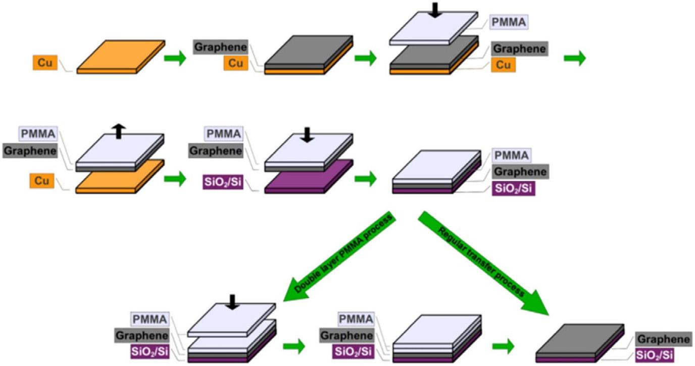
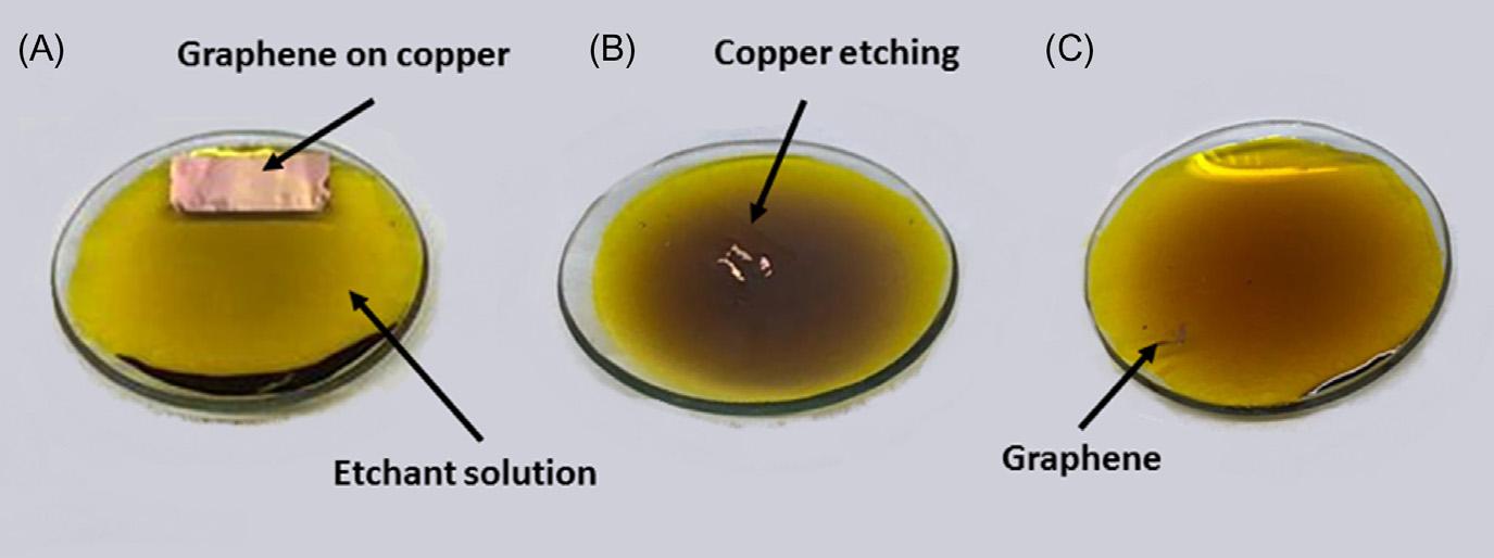
fact,thequalityofCVD-growngraphenedependscriticallyontheusedtransfer process.In Fig.1.8 anexampleusingthepoly(methylmethacrylate)(PMMA)basedtechniqueisdescribed.Inthisregularandquitestandardprocess,the PMMAisspincoatedonthegraphenesampleoncopper.Aftercoatingthesampleisannealedat80 Cfor15min.Inordertoetchthecopperfoil,thegraphene/ PMMAfilmthenisimmersedincopperetchant, Fig.1.9.Thesuspendedfilms aretransferredtodeionizedwater,where,subsequently,thegraphene/PMMA filmscanbetransferredontoSiO2/Sisubstrates(properlycleaned) [59].Theuse ofadouble-layerPMMA,assuggests,andthenanannealingsteptoremovethe PMMAlayerhavedemonstratedagraphenequalityimprovement [59]
Inordertoscalethegrowthandtransferprocesses,recentadvanceshavebeen achievedusingroll-to-rollmethodstogrowmeter-sizesingle-crystalgraphene afterrecrystallizingindustrialCu-to-Cu(111)foil [60].Regardingtheelectrical
FIGURE1.8
SchematicdiagramofgraphenetransferbasedonPMMAtechnique. PMMA,Poly(methyl methacrylate).
ReprintedfromG.B.Barin,etal.,Optimizedgraphenetransfer:influenceofpolymethylmethacrylate(PMMA) layerconcentrationandbakingtimeongraphenefinalperformance,Carbon84(2015)82 90, ©2015with permissionfromElsevier.
FIGURE1.9
(A)Graphene/copperfoils(1 3 2cm2)intheetchantsolutionofironchloride,FeCl3 in HCl/H2O(1M 5M),(B)after1hetching,(C)after2hetchingintheetchantsolution.
properties,transferreddeviceshavedemonstratedmobilitiesashighas 350,000cm2/Vs [61] beingcomparablewiththeseachievedinexfoliateddevices. Despitealltheseadvances,therearestillsomeissuesingraphenegrowthtobe resolved:thecontrolofthedomain(grain)size,ripples,dopinglevel,andthe numberoflayers.Simultaneously,thetransferprocessshouldbeimprovedand
optimizedwiththeobjectivesofminimizingthedamagetographeneandof recoveringthesacrificialmetal [62].
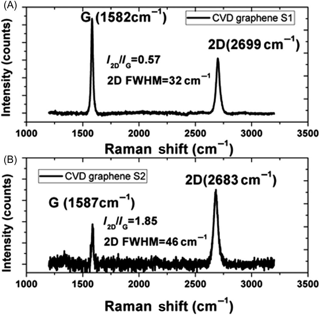
1.2.3 StructuralRamancharacterizationafterthesynthesis Ramanspectroscopyiswidelyusedtocharacterizegrapheneandrelatedmaterials.In fact,ingraphene,itisespeciallyuseful sinceduetotheabsenceofbandgapinthe material,allwavelengthsofincidentradiationresonant,thus theRamanspectrum containsinformationaboutbothatomicstructure(disorder,defects,andthickness) andelectronicproperties [63,64].ThemostimportantcharacteristicsofRamanspectrumingraphenearetheso-calledGand2Dmodes.Gmodeislocatedaround 1580cm 1 and2Dmodearound2700cm 1 [65].Asthenumberofgraphenelayers increase,thespectrumwillchangefrom single-layergraphenebysplittingthe2D peakintoanincreasingnumberofmodesthatcancombinetoformawider,shorter, higherfrequencypeak [66].TheGpeakalsoexperiencesasmallershiftfrom increasednumberoflayers.Thusthenumberoflayersofthefilmcanbederived fromtheratioofpeakintensities,I2D/IG,aswellasthepositionandshapeofthese peaks [64,66].ThiseffectiseasilyobservedinourCVD-synthesizedsamples.Two differentprocesseswithfewmodifications butsimilartotheonepreviouslydescribed (49)arecarriedouttosynthesizethesamples.Inthesampleof Fig.1.10A theH2 flowhasbeenheldduringtheannealing(60min)andthegrowth(30min)stages. Thecoolingstephastaken25min(slowcooling)andthepressurehassetto1Torr (133Pa).Theratio I2D/IG andthe2Dfullwidthathalfmaximumsuggestmultilayer graphene(aroundfourlayer).However, Fig.1.10B showsthespectrumofareaction wherethepressurehassetto0.5Torr(B66Pa),andtheannealingandgrowthstages havebeen30minlongeachone.NopresenceofH2 duringtheannealingstageanda fastcoolinghasbeenset, Fig.1.7B.Thespectrumof Fig.1.10B suggests,with I2D/ IGB2,athicknessclosetosingle-layergraphene.Theseresults,differentgraphene thicknessesdependingonthegrowthconditions,suggestatime-demandingtaskto achievethetargetthickness(tinychangesinthesynthesisconditionscanbecritical) andatthesametimethatdemonstratesthe versatilityoftheCVDprocess,controlling theconditions,differentgraphenelayerstructurescanbesynthesized.
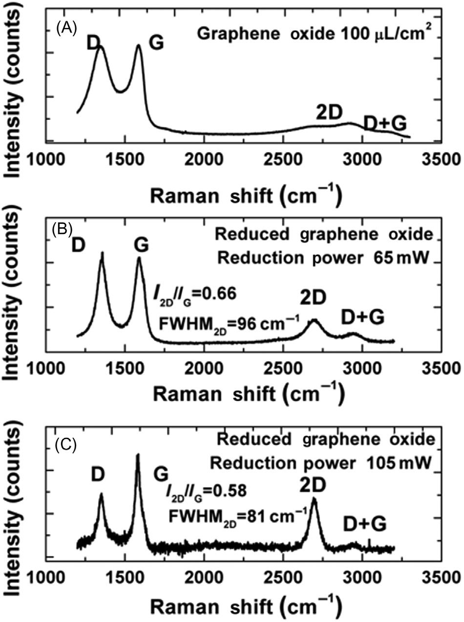
OtheradditionalpeaksmaybealsoobservedintheRamanspectrum:Dpeakat approximately1350cm 1,D0 around1620cm 1,G peakat2450cm 1,andD 1 G peakat2940cm 1,allrelatedtodisorderingraphene [65,67].TheDpeakofthe spectrumisnotvisibleinpristinegraphene,becauseitsactivationimpliesthatacarriermustbeexcitedandinelasticallyscatteredbyaphononandsubsequentlyasecondinelasticscatteringbyadefector azoneboundarymustoccurleadingto recombination.Moreover,theratioofpeakintensitiesID/IG canbeusedtocharacterizethelevelofdisorderingraphene [18,63,68].Theimplicationsofthesepeaksare shownin Fig.1.11 withgrapheneoxidereductionprocess. Fig.1.11A showsthe spectrumofgrapheneoxide,obtainedfollowingtheHummer’sapproachpreviously presented.Inthiscase,Dmodeissignificantlyintense(sometimesevenmorethan theGmode)duetothedistortioninducedinthesp2 structureoriginatedfromthe
FIGURE1.10
RamanspectraofCVDgraphenefilmgrownonaCusubstratefollowingtwodifferent conditionprocesses(Ramanlaserexcitationwavelength532nm).(A)Thespectrum showsmultilayergraphenestructurewitharoundfourlayers.(B)Spectrumwith I2D/IG rationsuggestingalmostsingle-layergraphene.TheabsenceofDpeaksuggestsfreedefectgraphene. CVD,Chemicalvapordeposition. 14CHAPTER1 Synthesisofgrapheneandothertwo-dimensionalmaterials
oxidativesynthesistogetherwiththehydroxylandepoxygroups.TheGpeakisand 2Dpeakisalmostnonexistent.Afterafirstreductionprocess,atlowlaserintensity, Fig.1.11B,Dpeakisattenuatedandthe2Dpeakincreases,asaconsequenceofthe partialrestorationofthecrystallographicstructureandthereductionofthenumberof defects.Thiseffectisevenmoreabruptwhenahigherlaserintensityisemployed, Fig.1.11C.Inthiscasethe I2D/IG andthe IG/ID ratiosimprove,determiningabetter restorationofthesemimetalstructure.However,asmentionedandthespectrumsuggests,withthisoxidation reductionmethod,single-layerfree-defectgraphenein largescaleisstillunrealizable.
1.3 Synthesisofothertwo-dimensionalmaterials Asmentionedin Section1.1,2Dlayeredmaterialsareemergingrapidlyoriginated fromtheirexceptionalchemicalandphysicalpropertiesthatarenotpresentintheir
FIGURE1.11
Ramanspectraofgrapheneoxide(A),lowpower(65mW)thermallyreducedgraphene oxide(B),andreducedgrapheneoxideatawavelengthof550nmand105mW(C).
bulkcounterparts [4].Althoughgraphenewasthefirsttoberealizedbymechanical exfoliationofgraphite [1],thereisaverywidespectrumof2Dcrystalsthatrange frominsulatorstosemiconductorsandmetals,withinterlayerinteractionsmainly governedbyvdWforces [69 71],thatis,h-BN [72],TMDs [73,74],transition metalcarbidesand/orcarbonnitrides(MXenes) [75 77],transitionmetaltrichalcogenidescomposedofeithergroup-IVBorgroup-VBtransitionmetalandchalcogen atoms [78,79],groupIII/IV VImonochalcogenides [80 85],chromiumtrihalides CrX3 (X 5 Cl,Br,I) [86 90],transitionmetal ternarycompounds [91 97],and mono-elemental2Dmaterials [98].Similartothecaseofthegraphenesynthesis, therearetwoprimarystrategiesforthefabricationof2Dmaterialswhichrelyon boththetop-downandthebottom-upapproaches.Inthissectionthemostcommonlyusedtop-downandbottom-upsynthesisstrategiesfocusedonthepreparation of2Dnanomaterialsareintroduced.