
Instructor's Resource Manual to accompany Electronic Devices And Circuit Theory (10th Ed.) 10th Edition
Robert L.Boylestead
Visit to download the full and correct content document: https://ebookmass.com/product/instructors-resource-manual-to-accompany-electronic -devices-and-circuit-theory-10th-ed-10th-edition-robert-l-boylestead/
More products digital (pdf, epub, mobi) instant download maybe you interests ...
Introductory Circuit Analysis (11th Ed.) - Instructor’s Resource Manual 11th Edition Robert L. Boylestad
https://ebookmass.com/product/introductory-circuit-analysis-11thed-instructors-resource-manual-11th-edition-robert-l-boylestad/

Instructor’s Solutions Manual to Solid State Electronic Devices, 6th Edition Ben G. Streetman
https://ebookmass.com/product/instructors-solutions-manual-tosolid-state-electronic-devices-6th-edition-ben-g-streetman/
Electronic Devices, Conventional Current Version 10th Edition Thomas L. Floyd
https://ebookmass.com/product/electronic-devices-conventionalcurrent-version-10th-edition-thomas-l-floyd/

Experiments Manual To Accompany Digital Electronics: Principles and Applications, 9th Edition Tokheim
https://ebookmass.com/product/experiments-manual-to-accompanydigital-electronics-principles-and-applications-9th-editiontokheim/

Electronic Devices and Circuits S. Salivahanan
https://ebookmass.com/product/electronic-devices-and-circuits-ssalivahanan/

Laboratory manual [to accompany] Physical examination & health assessment 7th Edition Edition Jarvis
https://ebookmass.com/product/laboratory-manual-to-accompanyphysical-examination-health-assessment-7th-edition-editionjarvis/
Introductory Circuit Analysis. (Global Edition) (14th Ed.) Robert L. Boylestad
https://ebookmass.com/product/introductory-circuit-analysisglobal-edition-14th-ed-robert-l-boylestad/
Solutions Manual to accompany An Introduction to Numerical Methods and Analysis James F. Epperson
https://ebookmass.com/product/solutions-manual-to-accompany-anintroduction-to-numerical-methods-and-analysis-james-f-epperson/
Student Solutions Manual to Accompany Atkins' Physical Chemistry 11th Edition Peter Bolgar
https://ebookmass.com/product/student-solutions-manual-toaccompany-atkins-physical-chemistry-11th-edition-peter-bolgar/
Instructor’s Resource Manual to accompany
Electronic Devices and Circuit Theory

Tenth Edition
Robert L. Boylestad Louis Nashelsky

Upper Saddle River, New Jersey Columbus, Ohio
Copyright © 2009 by Pearson Education, Inc., Upper Saddle River, New Jersey 07458.
Pearson Prentice Hall. All rights reserved. Printed in the United States of America. This publication is protected by Copyright and permission should be obtained from the publisher prior to any prohibited reproduction, storage in a retrieval system, or transmission in any form or by any means, electronic, mechanical, photocopying, recording, or likewise. For information regarding permission(s), write to: Rights and Permissions Department.
Pearson Prentice Hall™ is a trademark of Pearson Education, Inc.
Pearson® is a registered trademark of Pearson plc
Prentice Hall® is a registered trademark of Pearson Education, Inc.
Instructors of classes using Boylestad/Nashelsky, Electronic Devices and Circuit Theory, 10th edition, may reproduce material from the instructor’s text solutions manual for classroom use.

10 9 8 7 6 5 4 3 2 1
ISBN-13: 978-0-13-503865-9
ISBN-10: 0-13-503865-0
Chapter 1
1. Copper has 20 orbiting electrons with only one electron in the outermost shell. The fact that the outermost shell with its 29th electron is incomplete (subshell can contain 2 electrons) and distant from the nucleus reveals that this electron is loosely bound to its parent atom. The application of an external electric field of the correct polarity can easily draw this loosely bound electron from its atomic structure for conduction.
Both intrinsic silicon and germanium have complete outer shells due to the sharing (covalent bonding) of electrons between atoms. Electrons that are part of a complete shell structure require increased levels of applied attractive forces to be removed from their parent atom.
2. Intrinsic material: an intrinsic semiconductor is one that has been refined to be as pure as physically possible. That is, one with the fewest possible number of impurities.
Negative temperature coefficient: materials with negative temperature coefficients have decreasing resistance levels as the temperature increases.
Covalent bonding: covalent bonding is the sharing of electrons between neighboring atoms to form complete outermost shells and a more stable lattice structure.
3.
4. W = QV = (6 C)(3 V) = 18 J
5. 48 eV = 48(1.6 × 10 19 J) = 76.8 × 10 19 J
Q = W V = 19 76.810 J 12 V × = 6.40 × 10 19 C
6.4 × 10 19 C is the charge associated with 4 electrons.
6. GaP Gallium Phosphide Eg = 2.24 eV ZnS Zinc Sulfide Eg = 3.67 eV
7. An n-type semiconductor material has an excess of electrons for conduction established by doping an intrinsic material with donor atoms having more valence electrons than needed to establish the covalent bonding. The majority carrier is the electron while the minority carrier is the hole.
A p-type semiconductor material is formed by doping an intrinsic material with acceptor atoms having an insufficient number of electrons in the valence shell to complete the covalent bonding thereby creating a hole in the covalent structure. The majority carrier is the hole while the minority carrier is the electron.
8. A donor atom has five electrons in its outermost valence shell while an acceptor atom has only 3 electrons in the valence shell.
9. Majority carriers are those carriers of a material that far exceed the number of any other carriers in the material.
Minority carriers are those carriers of a material that are less in number than any other carrier of the material.
10. Same basic appearance as Fig. 1.7 since arsenic also has 5 valence electrons (pentavalent).
11. Same basic appearance as Fig. 1.9 since boron also has 3 valence electrons (trivalent). 12. 13.
14. For forward bias, the positive potential is applied to the p-type material and the negative potential to the n-type material.
15. TK = 20 + 273 = 293
k = 11,600/n = 11,600/2 (low value of VD) = 5800
ID = Is 1 D K kV T e ⎛⎞ ⎜⎟ ⎜⎟
= 50 × 10 9 (5800)(0.6) 293 1 e ⎛⎞
= 50 × 10 9 (e 11.877 1) = 7.197 mA
16. k = 11,600/n = 11,600/2 = 5800 (n = 2 for VD = 0.6 V)
TK = TC + 273 = 100 + 273 = 373 (5800)(0.6 V) / 9.33 373 kVTK eee == = 11.27 × 10³
I = / (1) kVTK s Ie = 5 μA(11.27 × 10³ 1) = 56.35 mA
17. (a) TK = 20 + 273 = 293 k = 11,600/n = 11,600/2 = 5800
ID = Is 1 D K kV T e ⎛⎞ ⎜⎟ ⎜⎟ ⎝⎠ = 0.1μA (5800)(10 V) 293 1 e ⎛⎞
= 0.1 × 10 6(e 197.95 1) = 0.1 × 10 6(1.07 × 10 86 1) ≅ 0.1 × 10 6 0.1μA
ID = Is = 0.1 μA
(b) The result is expected since the diode current under reverse-bias conditions should equal the saturation value.
18. (a) x y = e x 0 1 1 2.7182
2 7.389
3 20.086
4 54.6
5 148.4
(b) y = e 0 = 1
(c) For V = 0 V, e 0 = 1 and I = Is(1 1) = 0 mA
19. T = 20°C: Is = 0.1 μA
T = 30°C: Is = 2(0.1 μA) = 0.2 μA (Doubles every 10°C rise in temperature)
T = 40°C: Is = 2(0.2 μA) = 0.4 μA
T = 50°C: Is = 2(0.4 μA) = 0.8 μA
T = 60°C: Is = 2(0.8 μA) = 1.6 μA 1.6 μA: 0.1 μA ⇒ 16:1 increase due to rise in temperature of 40°C.
20. For most applications the silicon diode is the device of choice due to its higher temperature capability. Ge typically has a working limit of about 85 degrees centigrade while Si can be used at temperatures approaching 200 degrees centigrade. Silicon diodes also have a higher current handling capability. Germanium diodes are the better device for some RF small signal applications, where the smaller threshold voltage may prove advantageous.
21. From 1.19:
VF decreased with increase in temperature
1.1 V: 0.6 V ≅ 1.83:1 Is increased with increase in temperature 1.05 μA: 0.01 pA = 105 × 103:1
22. An “ideal” device or system is one that has the characteristics we would prefer to have when using a device or system in a practical application. Usually, however, technology only permits a close replica of the desired characteristics. The “ideal” characteristics provide an excellent basis for comparison with the actual device characteristics permitting an estimate of how well the device or system will perform. On occasion, the “ideal” device or system can be assumed to obtain a good estimate of the overall response of the design. When assuming an “ideal” device or system there is no regard for component or manufacturing tolerances or any variation from device to device of a particular lot.
23. In the forward-bias region the 0 V drop across the diode at any level of current results in a resistance level of zero ohms – the “on” state – conduction is established. In the reverse-bias region the zero current level at any reverse-bias voltage assures a very high resistance level the open circuit or “off” state conduction is interrupted.
24. The most important difference between the characteristics of a diode and a simple switch is that the switch, being mechanical, is capable of conducting current in either direction while the diode only allows charge to flow through the element in one direction (specifically the direction defined by the arrow of the symbol using conventional current flow).
25. VD ≅ 0.66 V, ID = 2 mA
RDC = 0.65 V 2 mA D D V I = = 325 Ω
26. At ID = 15 mA, VD = 0.82 V
RDC = 0.82 V 15 mA D D V I = = 54.67 Ω
As the forward diode current increases, the static resistance decreases.
27. VD = 10 V, ID = Is = 0.1 μA
RDC = 10 V 0.1 A D D V I μ = = 100 MΩ
VD = 30 V, ID = Is= 0.1 μA
RDC = 30 V 0.1A D D V I μ = = 300 MΩ
As the reverse voltage increases, the reverse resistance increases directly (since the diode leakage current remains constant).
28. (a) rd = 0.79 V0.76 V0.03V 15 mA5mA10 mA d d V I Δ == Δ− = 3 Ω
(b) rd = 26 mV26 mV 10 mA ID = = 2.6 Ω
(c) quite close
29. ID = 10 mA, VD = 0.76 V
RDC = 0.76 V 10 mA D D V I = = 76 Ω
rd = 0.79 V0.76 V0.03 V 15 mA 5 mA10 mA d d V I Δ ≅= Δ− = 3 Ω
RDC >> rd
30. ID = 1 mA, rd = 0.72 V0.61 V 2 mA0mA d d V I Δ = Δ− = 55 Ω
ID = 15 mA, rd = 0.8 V0.78 V 20 mA10mA d d V I Δ = Δ− = 2 Ω
31. ID = 1 mA, rd = 26 mV 2 ID ⎛⎞ ⎜⎟ ⎝⎠ = 2(26 Ω) = 52 Ω vs 55 Ω (#30)
ID = 15 mA, rd = 26 mV26 mV 15 mA ID = = 1.73 Ω vs 2 Ω (#30)
32. rav = 0.9 V0.6 V 13.5 mA1.2mA d d V I Δ = Δ− = 24.4 Ω
33. rd = 0.8 V0.7 V0.09 V 7 mA 3 mA4 mA
d d V I Δ ≅= Δ− = 22.5 Ω (relatively close to average value of 24.4 Ω (#32))
34. rav = 0.9 V0.7 V0.2 V 14 mA0mA14 mA
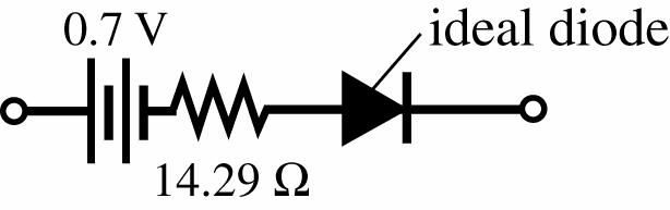
d d V I Δ == Δ− = 14.29 Ω
35. Using the best approximation to the curve beyond VD = 0.7 V: rav = 0.8 V0.7 V0.1 V 25 mA 0 mA25 mA d d V I Δ ≅= Δ− = 4 Ω
36. (a) VR = 25 V: CT ≅ 0.75 pF
VR = 10 V: CT ≅ 1.25 pF
1.25 pF0.75 pF0.5pF 10 V 25 V15 V T R C V Δ == Δ− = 0.033 pF/V
(b) VR = 10 V: CT ≅ 1.25 pF
VR = 1 V: CT ≅ 3 pF 1.25 pF3 pF1.75pF 10 V 1 V9 V T R C V Δ == Δ− = 0.194 pF/V
(c) 0.194 pF/V: 0.033 pF/V = 5.88:1 ≅ 6:1 Increased sensitivity near VD = 0 V
37. From Fig. 1.33
VD = 0 V, CD = 3.3 pF
VD = 0.25 V, CD = 9 pF
38. The transition capacitance is due to the depletion region acting like a dielectric in the reversebias region, while the diffusion capacitance is determined by the rate of charge injection into the region just outside the depletion boundaries of a forward-biased device. Both capacitances are present in both the reverse- and forward-bias directions, but the transition capacitance is the dominant effect for reverse-biased diodes and the diffusion capacitance is the dominant effect for forward-biased conditions.
39. VD = 0.2 V, CD = 7.3 pF
XC = 11 22(6 MHz)(7.3 pF) fC ππ = = 3.64 kΩ
VD = 20 V, CT = 0.9 pF
XC = 11 22(6 MHz)(0.9 pF) fC ππ = = 29.47 kΩ
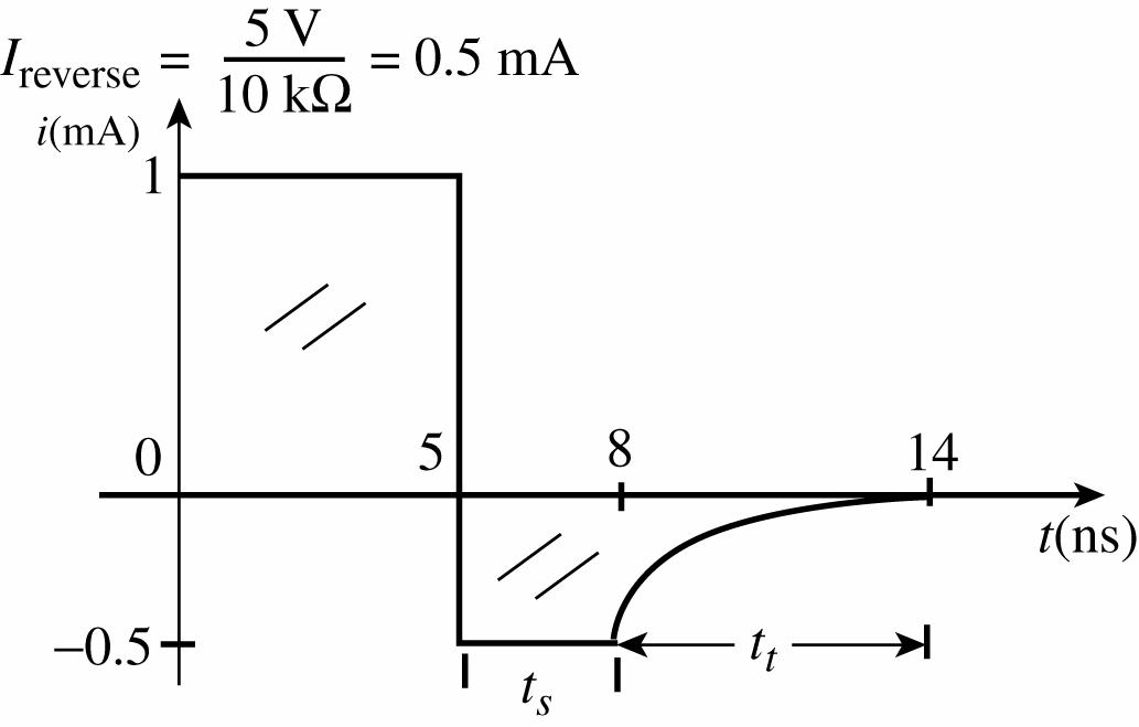
40. If = 10 V 10 kΩ = 1 mA
ts + tt = trr = 9 ns
ts + 2ts = 9 ns
ts = 3 ns
tt = 2ts = 6 ns
42. As the magnitude of the reverse-bias potential increases, the capacitance drops rapidly from a level of about 5 pF with no bias. For reverse-bias potentials in excess of 10 V the capacitance levels off at about 1.5 pF.
43. At VD = 25 V, ID = 0.2 nA and at VD = 100 V, ID ≅ 0.45 nA. Although the change in IR is more than 100%, the level of IR and the resulting change is relatively small for most applications.
44. Log scale: TA = 25°C, IR = 0.5 nA
TA = 100°C, IR = 60 nA
The change is significant.
60 nA: 0.5 nA = 120:1
Yes, at 95°C IR would increase to 64 nA starting with 0.5 nA (at 25°C) (and double the level every 10°C).
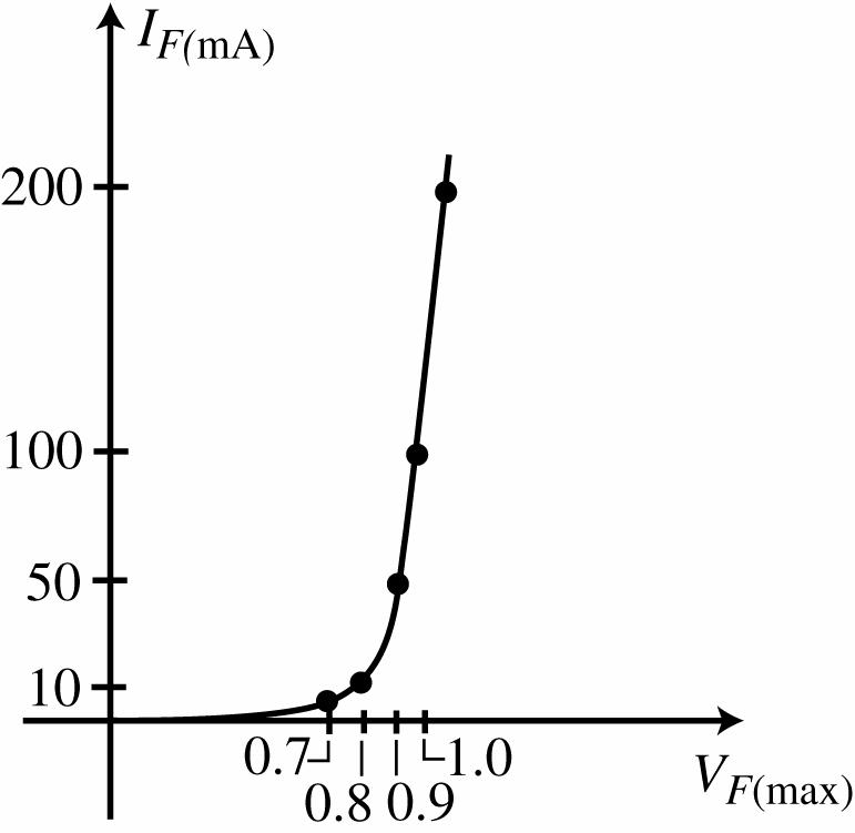
45. IF = 0.1 mA: rd ≅ 700 Ω
IF = 1.5 mA: rd ≅ 70 Ω
IF = 20 mA: rd ≅ 6 Ω
The results support the fact that the dynamic or ac resistance decreases rapidly with increasing current levels.
46. T = 25°C: Pmax = 500 mW
T = 100°C: Pmax = 260 mW Pmax = VFIF
IF = max 500 mW 0.7 V F P V = = 714.29 mA
IF = max 260 mW 0.7 V F P V = = 371.43 mA
714.29 mA: 371.43 mA = 1.92:1 ≅ 2:1
47. Using the bottom right graph of Fig. 1.37: IF = 500 mA @ T = 25°C At IF = 250 mA, T ≅ 104°C
48.
49. TC = +0.072% = 10 100% () Z Z V VTT Δ × 0.072 = 1 0.75V 100 10V(25) T × 0.072 = 1 7.5 25 T T1 25° = 7.5 0.072 = 104.17° T1 = 104.17° + 25° = 129.17°
50. TC = 10 () Z Z V VTT Δ × 100% = (5 V 4.8 V) 5V(10025) °−° × 100% = 0.053%/°C
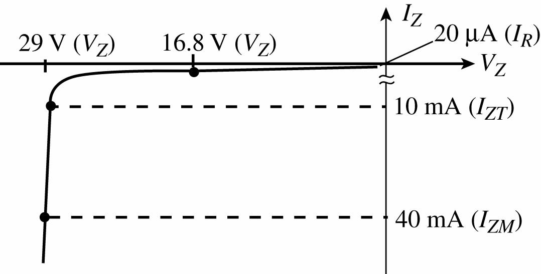
51. (20 V 6.8 V)
(24 V 6.8 V) × 100% = 77%
The 20 V Zener is therefore ≅ 77% of the distance between 6.8 V and 24 V measured from the 6.8 V characteristic.
At IZ = 0.1 mA, TC ≅ 0.06%/°C
(5 V 3.6 V)
(6.8 V 3.6 V) × 100% = 44%
The 5 V Zener is therefore ≅ 44% of the distance between 3.6 V and 6.8 V measured from the 3.6 V characteristic.
At IZ = 0.1 mA, TC ≅ 0.025%/°C
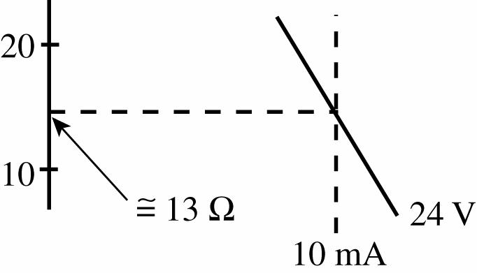
53. 24 V Zener:
0.2 mA: ≅ 400 Ω
1 mA: ≅ 95 Ω
10 mA: ≅ 13 Ω
The steeper the curve (higher dI/dV) the less the dynamic resistance.
54. VT ≅ 2.0 V, which is considerably higher than germanium (≅ 0.3 V) or silicon (≅ 0.7 V). For germanium it is a 6.7:1 ratio, and for silicon a 2.86:1 ratio.
55. Fig. 1.53 (f) IF ≅ 13 mA
Fig. 1.53 (e) VF ≅ 2.3 V
56. (a) Relative efficiency @ 5 mA ≅ 0.82 @ 10 mA ≅ 1.02
1.020.82 0.82 × 100% = 24.4% increase
ratio: 1.02 0.82 = 1.24
(b) Relative efficiency @ 30 mA ≅ 1.38 @ 35 mA ≅ 1.42
1.421.38 1.38 × 100% = 2.9% increase
ratio: 1.42 1.38 = 1.03
(c) For currents greater than about 30 mA the percent increase is significantly less than for increasing currents of lesser magnitude.
57. (a) 0.75 3.0 = 0.25
From Fig. 1.53 (i) ≅ 75°
(b) 0.5 ⇒ = 40 °
58. For the high-efficiency red unit of Fig. 1.53:
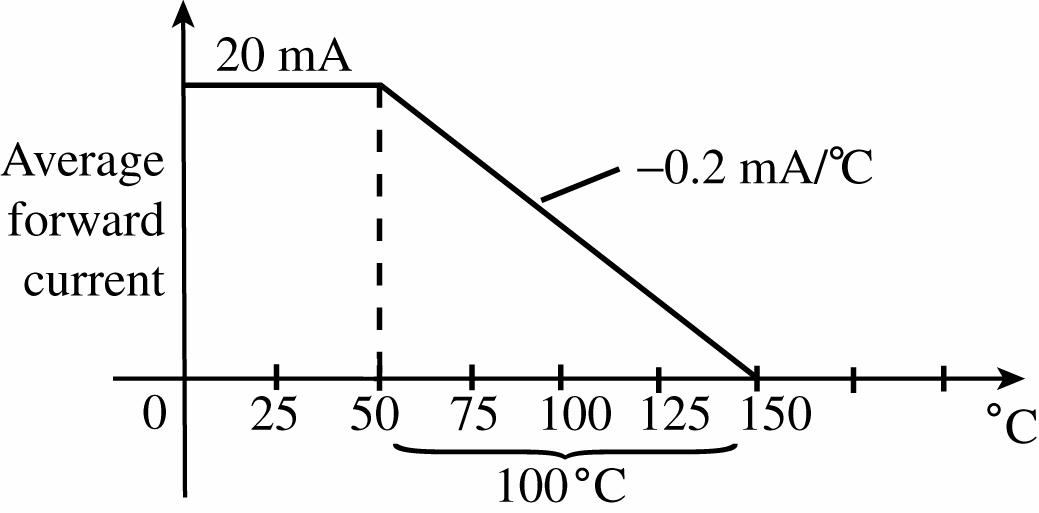
0.2 mA20 mA
C x = ° x = 20 mA
0.2 mA/C ° = 100°C
Chapter 2
1. The load line will intersect at ID = 8 V 330 E R = Ω = 24.24 mA and VD = 8 V.
(a) VDQ ≅ 0.92 V
IDQ ≅ 21.5 mA
VR = E VDQ = 8 V 0.92 V = 7.08 V
(b) VDQ ≅ 0.7 V
IDQ ≅ 22.2 mA
VR = E VDQ = 8 V 0.7 V = 7.3 V
(c) VDQ ≅ 0 V
IDQ ≅ 24.24 mA
VR = E VDQ = 8 V 0 V = 8 V
For (a) and (b), levels of VDQ and IDQ are quite close. Levels of part (c) are reasonably close but as expected due to level of applied voltage E
2. (a) ID = 5 V 2.2 k E R = Ω = 2.27 mA
The load line extends from ID = 2.27 mA to VD = 5 V.
VDQ ≅ 0.7 V, IDQ ≅ 2 mA
(b) ID = 5 V 0.47 k E R = Ω = 10.64 mA
The load line extends from ID = 10.64 mA to VD = 5 V.
VDQ ≅ 0.8 V, IDQ ≅ 9 mA
(c) ID = 5 V 0.18 k E R = Ω = 27.78 mA
The load line extends from ID = 27.78 mA to VD = 5 V.
VDQ ≅ 0.93 V, IDQ ≅ 22.5 mA
The resulting values of VDQ are quite close, while IDQ extends from 2 mA to 22.5 mA.
3. Load line through IDQ = 10 mA of characteristics and VD = 7 V will intersect ID axis as 11.25 mA.
ID = 11.25 mA = 7 V E R R =
with R = 7 V 11.25 mA = 0.62 kΩ
4. (a) ID = IR = 30 V0.7 V 2.2 k EVD R = Ω = 13.32 mA
VD = 0.7 V, VR = E VD = 30 V 0.7 V = 29.3 V
(b) ID = 30V0V 2.2 k EVD R = Ω = 13.64 mA
VD = 0 V, VR = 30 V
Yes, since E VT the levels of ID and VR are quite close.
5. (a) I = 0 mA; diode reverse-biased.
(b) V20Ω = 20 V 0.7 V = 19.3 V (Kirchhoff’s voltage law) I = 19.3 V 20 Ω = 0.965 A
(c) I = 10 V 10 Ω = 1 A; center branch open
6. (a) Diode forward-biased, Kirchhoff’s voltage law (CW): 5 V + 0.7 V Vo = 0 Vo = 4.3 V IR = ID = 4.3 V 2.2 k o V R = Ω = 1.955 mA
(b) Diode forward-biased, ID = 8 V0.7 V 1.2 k4.7 k Ω+Ω = 1.24 mA
Vo = V4.7 kΩ + VD = (1.24 mA)(4.7 kΩ) + 0.7 V = 6.53 V
7. (a) Vo = 2 k(20 V 0.7V0.3V) 2 k2 k Ω−− Ω+Ω = 1 2 (20 V – 1 V) = 1 2 (19 V) = 9.5 V
(b) I = 10 V2V 0.7 V)11.3 V 1.2 k4.7 k5.9k +− = Ω+ΩΩ = 1.915 mA
V ′ = IR = (1.915 mA)(4.7 kΩ) = 9 V Vo = V ′ 2 V = 9 V 2 V = 7 V
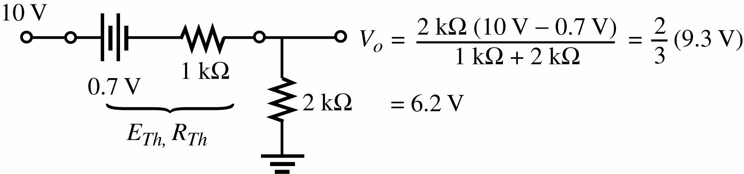
8. (a) Determine the Thevenin equivalent circuit for the 10 mA source and 2.2 kΩ resistor.
ETh = IR = (10 mA)(2.2 kΩ) = 22 V
RTh = 2. 2kΩ
(b) Diode forward-biased
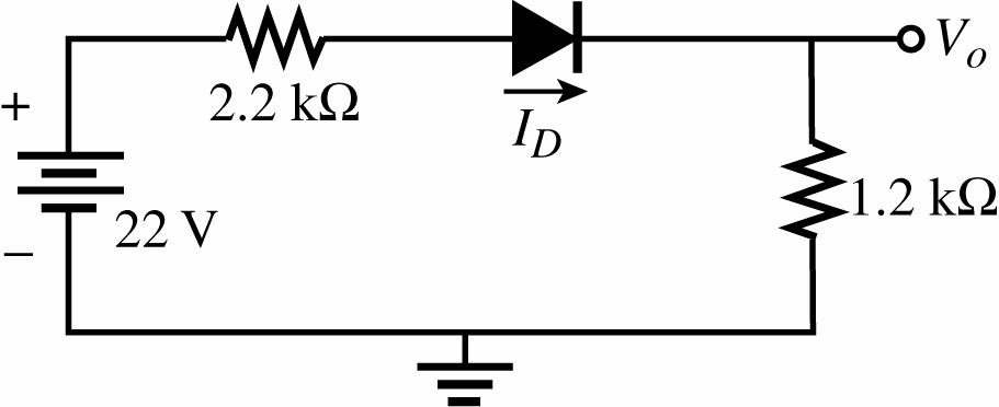
ID = 20 V + 5 V 0.7 V 6.8 kΩ = 2.65 mA
Kirchhoff’s voltage law (CW): +Vo 0.7 V + 5 V = 0 Vo = 4.3 V
9. (a) 1o V = 12 V – 0.7 V = 11.3 V
2o V = 0.3 V
(b)
Diode forward-biased
ID = 22 V0.7 V 2.2 k1.2 k Ω +Ω = 6.26 mA
Vo = ID(1.2 kΩ) = (6.26 mA)(1.2 kΩ) = 7.51 V
1o V = 10 V + 0.3 V + 0.7 V = 9 V I = 10 V0.7 V0.3 V9 V 1.2 k3.3k4.5 k = Ω+ΩΩ = 2 mA, 2o V = (2 mA)(3.3 kΩ) = 6.6 V
10. (a) Both diodes forward-biased
IR = 20 V0.7 V 4.7 kΩ = 4.106 mA
Assuming identical diodes: ID = 4.106 mA 22 IR = = 2.05 mA
Vo = 20 V 0.7 V = 19.3 V
(b) Right diode forward-biased:
ID = 15 V + 5 V0.7 V 2.2 kΩ = 8.77 mA
Vo = 15 V 0.7 V = 14.3 V
11. (a) Ge diode “on” preventing Si diode from turning “on”:
I = 10 V0.3 V9.7 V 1 k1 k = ΩΩ = 9.7 mA
(b) I = 16 V0.7 V0.7 V12 V2.6 V 4.7 k4.7 k = ΩΩ = 0.553 mA
Vo = 12 V + (0.553 mA)(4.7 kΩ) = 14.6 V
12. Both diodes forward-biased:
1o V = 0.7 V, 2o V = 0.3 V
I1 kΩ = 20 V 0.7 V 1 kΩ = 19.3 V 1 kΩ = 19.3 mA
I0.47 kΩ = 0.7 V0.3 V 0.47 kΩ = 0.851 mA
I(Si diode) = I1 kΩ I0.47 kΩ = 19.3 mA 0.851 mA = 18.45 mA
13. For the parallel Si 2 kΩ branches a Thevenin equivalent will result (for “on” diodes) in a single series branch of 0.7 V and 1 kΩ resistor as shown below:
I2 kΩ = 6.2 V 2 kΩ = 3.1 mA
ID = 2 k 3.1 mA 22 I Ω = = 1.55 mA
14. Both diodes “off”. The threshold voltage of 0.7 V is unavailable for either diode. Vo = 0 V
15. Both diodes “on”, Vo = 10 V 0.7 V = 9.3 V
16. Both diodes “on”. Vo = 0.7 V
17. Both diodes “off”, Vo = 10 V
18. The Si diode with 5 V at the cathode is “on” while the other is “off”. The result is Vo = 5 V + 0.7 V = 4.3 V
19. 0 V at one terminal is “more positive” than 5 V at the other input terminal. Therefore assume lower diode “on” and upper diode “off”.
The result:
Vo = 0 V 0.7 V = 0.7 V
The result supports the above assumptions.
20. Since all the system terminals are at 10 V the required difference of 0.7 V across either diode cannot be established. Therefore, both diodes are “off” and Vo = +10 V as established by 10 V supply connected to 1 kΩ resistor.
21. The Si diode requires more terminal voltage than the Ge diode to turn “on”. Therefore, with 5 V at both input terminals, assume Si diode “off” and Ge diode “on”.
The result: Vo = 5 V 0.3 V = 4.7 V
The result supports the above assumptions.
23. Using Vdc ≅ 0.318(Vm VT)
2 V = 0.318(Vm 0.7 V)
Solving: Vm = 6.98 V ≅ 10:1 for Vm:VT
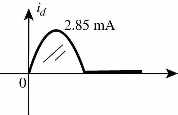
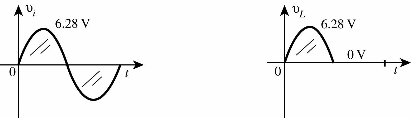
24. Vm = dc 2 V 0.3180.318 V = = 6.28 V
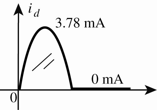
Imax(2.2 kΩ) = 6.28 V 2.2 kΩ = 2.855 mA
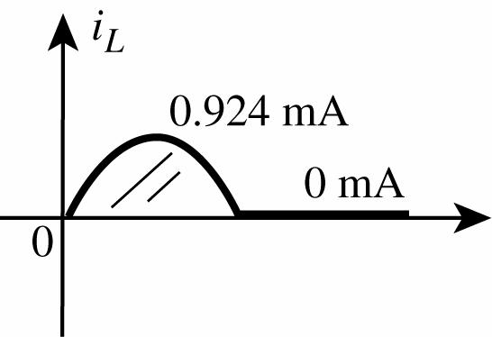
IIDL = + Imax(2.2 kΩ) = 0.924 mA + 2.855 mA = 3.78 mA
maxmax
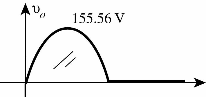
25. Vm = 2 (110 V) = 155.56 V
Vdc = 0.318Vm = 0.318(155.56 V) = 49.47 V
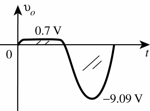
26. Diode will conduct when vo = 0.7 V; that is,
vo = 0.7 V = 10 k() 10 k1 k vi Ω Ω+Ω
Solving: vi = 0.77 V
For vi ≥ 0.77 V Si diode is “on” and vo = 0.7 V.
For vi < 0.77 V Si diode is open and level of vo is determined by voltage divider rule:
vo = 10 k() 10 k1 k vi Ω Ω+Ω = 0.909 vi
For vi = 10 V:
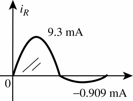
vo = 0.909( 10 V) = 9.09 V
When vo = 0.7 V, maxmaxR vvi = 0.7 V = 10 V 0.7 V = 9.3 V max 9.3 V 1 k IR = Ω = 9.3 mA
Imax(reverse) = 10 V 1 k10 k Ω+Ω = 0.909 mA
27. (a) Pmax = 14 mW = (0.7 V)ID
ID = 14 mW 0.7 V = 20 mA
(b) 4.7 kΩ || 56 kΩ = 4.34 kΩ
VR = 160 V 0.7 V = 159.3 V Imax = 159.3 V 4.34 kΩ = 36.71 mA
(c) Idiode = max 36.71 mA 22 I = = 18.36 mA
(d) Yes, ID = 20 mA > 18.36 mA
(e) Idiode = 36.71 mA Imax = 20 mA
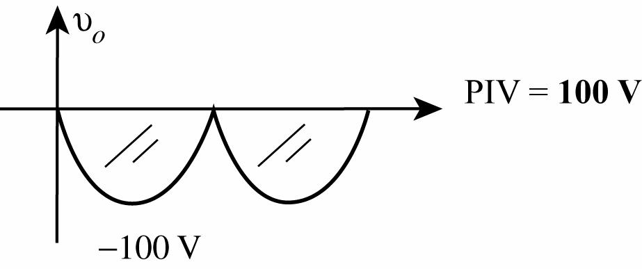
28. (a) Vm = 2(120 V) = 169.7 V VLm = Vim 2VD = 169.7 V 2(0.7 V) = 169.7 V 1.4 V = 168.3 V Vdc = 0.636(168.3 V) = 107.04 V
(b) PIV = Vm(load) + VD = 168.3 V + 0.7 V = 169 V
(c) ID(max) = 168.3 V 1 k Lm L V R = Ω = 168.3 mA
(d) Pmax = VDID = (0.7 V)Imax = (0.7 V)(168.3 mA) = 117.81 mW
29.
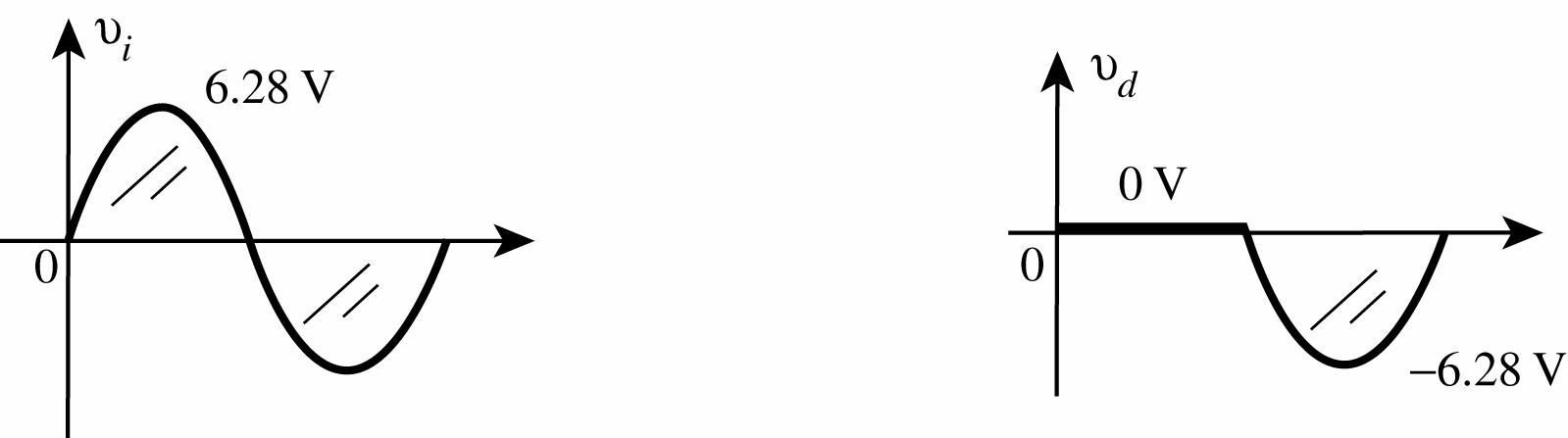
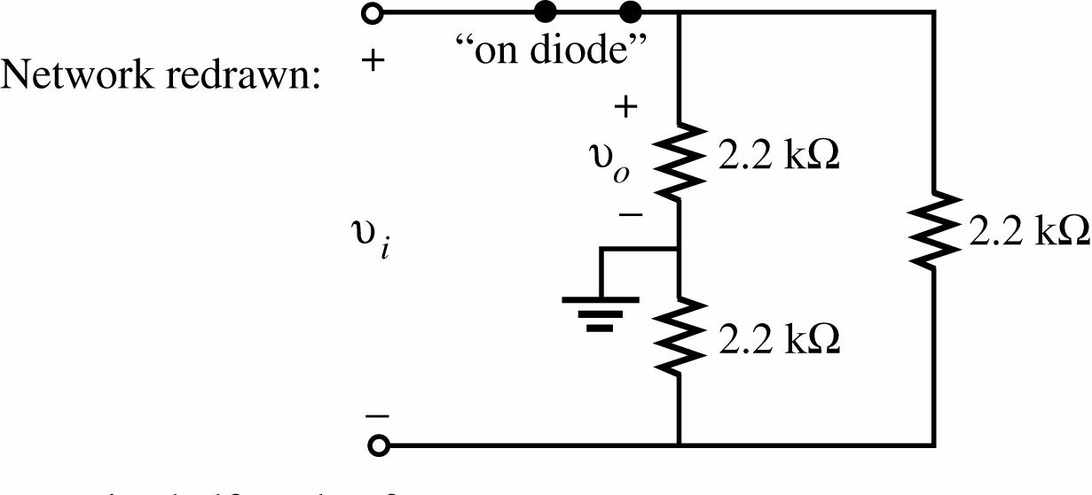
30. Positive half-cycle of vi:
31. Positive pulse of vi:
Voltage-divider rule:
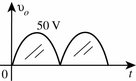
maxo V = max 2.2 k() 2.2 k2.2 k Vi Ω Ω+Ω = max 1 () 2 Vi = 1 (100 V) 2 = 50 V
Polarity of vo across the 2.2 kΩ resistor acting as a load is the same.
Voltage-divider rule:
maxo V = max 2.2 k()
2.2 k2.2 k Vi Ω Ω+Ω = max 1 () 2 Vi = 1 (100 V) 2 = 50 V Vdc = 0.636Vm = 0.636 (50 V) = 31.8 V
Top left diode “off”, bottom left diode “on”
2.2 kΩ || 2.2 kΩ = 1.1 kΩ
peako V = 1.1 k(170V)
1.1 k2.2 k Ω Ω +Ω = 56.67 V
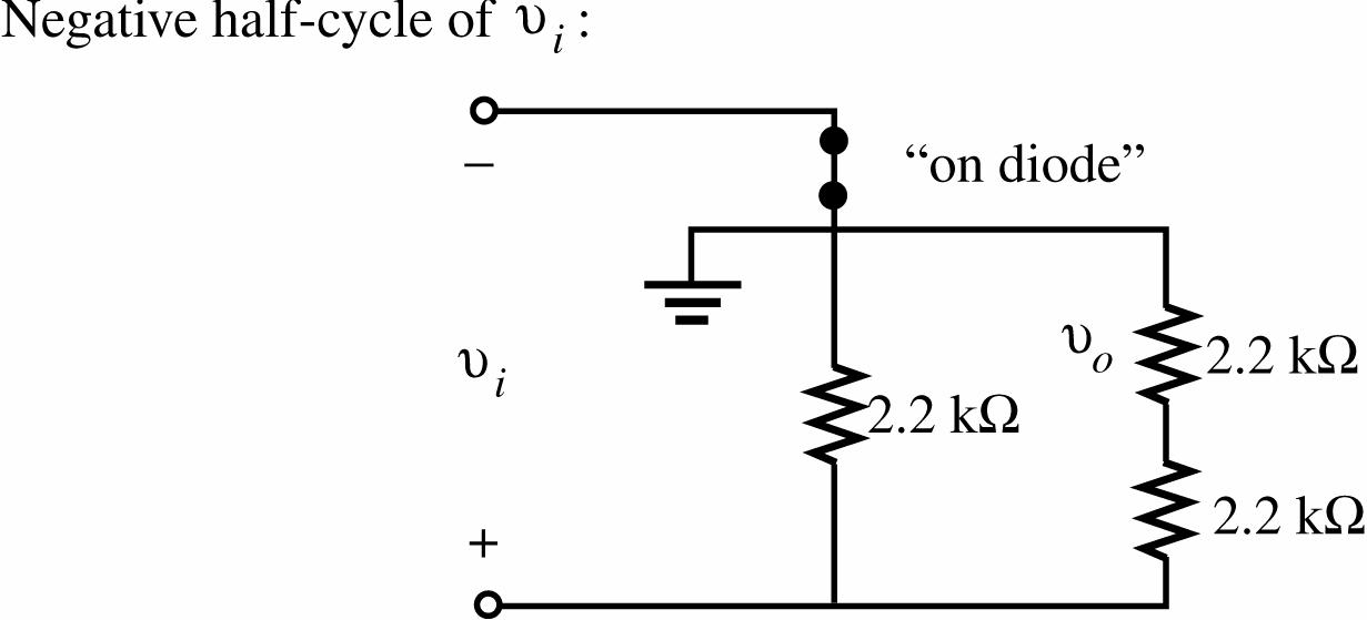
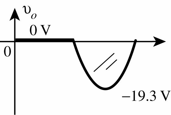
Negative pulse of vi:
Top left diode “on”, bottom left diode “off”
peako V = 1.1 k(170V)
1.1 k2.2 k Ω Ω +Ω = 56.67 V Vdc = 0.636(56.67 V) = 36.04 V
32. (a) Si diode open for positive pulse of vi and vo = 0 V For 20 V < vi ≤ 0.7 V diode “on” and vo = vi + 0.7 V. For vi = 20 V, vo = 20 V + 0.7 V = 19.3 V For vi = 0.7 V, vo = 0.7 V + 0.7 V = 0 V
(b) For vi ≤ 5 V the 5 V battery will ensure the diode is forward-biased and vo = vi 5 V.
At vi = 5 V
vo = 5 V 5 V = 0 V
At vi = 20 V
vo = 20 V 5 V = 25 V
For vi > 5 V the diode is reverse-biased and vo = 0 V
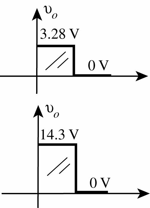
33. (a) Positive pulse of vi:
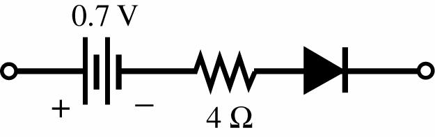
Vo = 1.2 k(10 V0.7 V) 1.2 k2.2 k Ω− Ω+Ω = 3.28 V
Negative pulse of vi: diode “open”, vo = 0 V
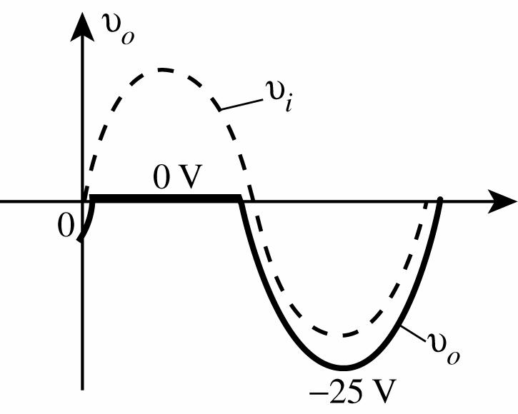
(b) Positive pulse of vi:
Vo = 10 V 0.7 V + 5 V = 14.3 V
Negative pulse of vi: diode “open”, vo = 0 V
34. (a) For vi = 20 V the diode is reverse-biased and vo = 0 V. For vi = 5 V, vi overpowers the 2 V battery and the diode is “on”.
Applying Kirchhoff’s voltage law in the clockwise direction:
5 V + 2 V vo = 0 vo = 3 V

(b) For vi = 20 V the 20 V level overpowers the 5 V supply and the diode is “on”. Using the short-circuit equivalent for the diode we find vo = vi = 20 V
For vi = 5 V, both vi and the 5 V supply reverse-bias the diode and separate vi from vo However, vo is connected directly through the 2.2 kΩ resistor to the 5 V supply and vo = 5 V
35. (a) Diode “on” for vi ≥ 4.7 V
For vi > 4.7 V, Vo = 4 V + 0.7 V = 4.7 V
For vi < 4.7 V, diode “off” and vo = vi
(b) Again, diode “on” for vi ≥ 4.7 V but vo now defined as the voltage across the diode
For vi ≥ 4.7 V, vo = 0.7 V
For vi < 4.7 V, diode “off”, ID = IR = 0 mA and V2.2 kΩ = IR = (0 mA)R = 0 V
Therefore, vo = vi 4 V
At vi = 0 V, vo = 4 V
vi = 8 V, vo = 8 V 4 V = 12 V
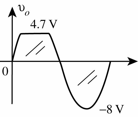
36. For the positive region of vi:
The right Si diode is reverse-biased. The left Si diode is “on” for levels of vi greater than 5.3 V + 0.7 V = 6 V. In fact, vo = 6 V for vi ≥ 6 V.
For vi < 6 V both diodes are reverse-biased and vo = vi
For the negative region of vi:
The left Si diode is reverse-biased. The right Si diode is “on” for levels of vi more negative than 7.3 V + 0.7 V = 8 V. In fact, vo = 8 V for vi ≤ 8 V.
For vi > 8 V both diodes are reverse-biased and vo = vi.
iR: For 8 V < vi < 6 V there is no conduction through the 10 kΩ resistor due to the lack of a complete circuit. Therefore, iR = 0 mA.
For vi ≥ 6 V
vR = vi vo = vi 6 V
For vi = 10 V, vR = 10 V 6 V = 4 V and iR = 4 V 10 kΩ = 0.4 mA
For vi ≤ 8 V
vR = vi vo = vi + 8 V
For vi = 10 V
vR = 10 V + 8 V = 2 V and iR = 2V 10 kΩ = 0.2 mA
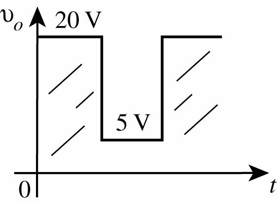
37. (a) Starting with vi = 20 V, the diode is in the “on” state and the capacitor quickly charges to 20 V+. During this interval of time vo is across the “on” diode (short-current equivalent) and vo = 0 V.
When vi switches to the +20 V level the diode enters the “off” state (open-circuit equivalent) and vo = vi + vC = 20 V + 20 V = +40 V
(b) Starting with vi = 20 V, the diode is in the “on” state and the capacitor quickly charges up to 15 V+. Note that vi = +20 V and the 5 V supply are additive across the capacitor. During this time interval vo is across “on” diode and 5 V supply and vo = 5 V.
When vi switches to the +20 V level the diode enters the “off” state and vo = vi + vC = 20 V + 15 V = 35 V.
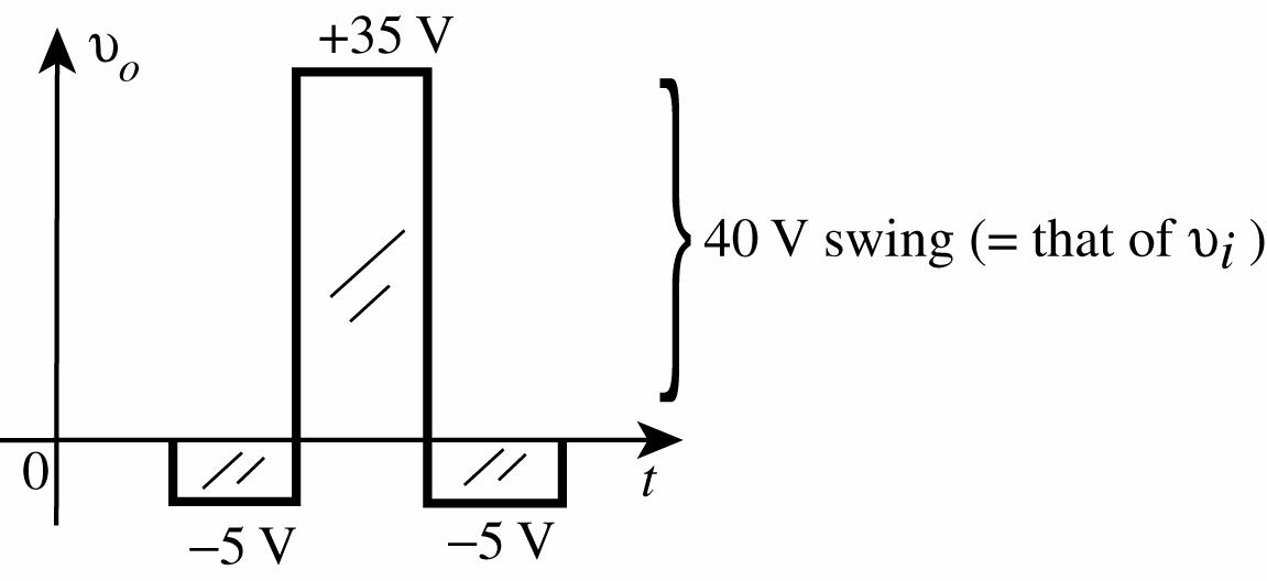
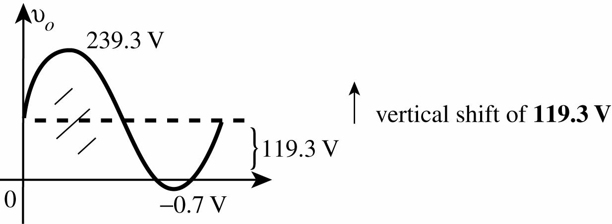
38. (a) For negative half cycle capacitor charges to peak value of 120 V 0.7 V = 119.3 V with polarity . The output vo is directly across the “on” diode resulting in vo = 0.7 V as a negative peak value. For next positive half cycle vo = vi + 119.3 V with peak value of vo = 120 V + 119.3 V = 239.3 V
(b) For positive half cycle capacitor charges to peak value of 120 V 20 V 0.7 V = 99.3 V with polarity . The output vo = 20 V + 0.7 V = 20.7 V For next negative half cycle vo = vi 99.3 V with negative peak value of vo = 120 V 99.3 V = 219.3 V.
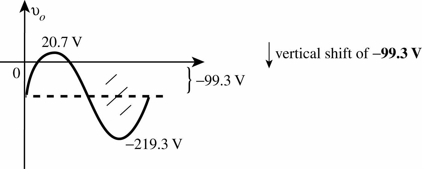
Using the ideal diode approximation the vertical shift of part (a) would be 120 V rather than 119.3 V and 100 V rather than 99.3 V for part (b). Using the ideal diode approximation would certainly be appropriate in this case.
39. (a) τ = RC = (56 kΩ)(0.1 μF) = 5.6 ms 5τ = 28 ms
(b) 5τ = 28 ms 2 T = 1 ms 2 = 0.5 ms, 56:1
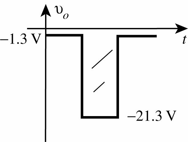
(c) Positive pulse of vi: Diode “on” and vo = 2 V + 0.7 V = 1.3 V
Capacitor charges to 10 V + 2 V 0.7 V = 11.3 V
Negative pulse of vi: Diode “off” and vo = 10 V 11.3 V = 21.3 V
40. Solution is network of Fig. 2.176(b) using a 10 V supply in place of the 5 V source.
41. Network of Fig. 2.178 with 2 V battery reversed.
42. (a) In the absence of the Zener diode
VL = 180(20 V)
180220 Ω Ω+Ω = 9 V
VL = 9 V < VZ = 10 V and diode non-conducting
Therefore, IL = IR = 20 V 220180Ω+Ω = 50 mA
with IZ = 0 mA and VL = 9 V
(b) In the absence of the Zener diode
VL = 470(20 V)
470220 Ω Ω+Ω = 13.62 V
VL = 13.62 V > VZ = 10 V and Zener diode “on”
Therefore, VL = 10 V and VRs = 10 V /10 V/220
ss RRs IVR==Ω = 45.45 mA
IL = VL/RL = 10 V/470 Ω = 21.28 mA and IZ = IRs IL = 45.45 mA 21.28 mA = 24.17 mA
(c) max PZ = 400 mW = VZIZ = (10 V)(IZ)
IZ = 400 mW 10 V = 40 mA
minIL = max s IIRZ = 45.45 mA 40 mA = 5.45 mA
RL = min 10 V 5.45 mA L L V I = = 1,834.86 Ω
Large RL reduces IL and forces more of IRs to pass through Zener diode.
(d) In the absence of the Zener diode
VL = 10 V = (20 V) 220 L L R R +Ω
10RL + 2200 = 20RL
10RL = 2200
RL = 220 Ω
43. (a) VZ = 12 V, RL = 12 V 200 mA L L V I = = 60 Ω
VL = VZ = 12 V = 60(16 V) 60 Li Lss RV R RR Ω = +Ω+
720 + 12Rs = 960 12Rs = 240 Rs = 20 Ω
(b) max PZ = VZ max IZ = (12 V)(200 mA) = 2.4 W
44. Since IL = LZ LL VV R R = is fixed in magnitude the maximum value of IRs will occur when IZ is a maximum. The maximum level of IRs will in turn determine the maximum permissible level of Vi. max max 400mW 8 V Z Z Z P I V == = 50 mA IL = 8 V 220 LZ LL VV RR == Ω = 36.36 mA
IRs = IZ + IL = 50 mA + 36.36 mA = 86.36 mA
s iZ R s VV I R = or Vi = Rs s IR + VZ = (86.36 mA)(91 Ω) + 8 V = 7.86 V + 8 V = 15.86 V
Any value of vi that exceeds 15.86 V will result in a current IZ that will exceed the maximum value.
45. At 30 V we have to be sure Zener diode is “on”.
∴ VL = 20 V = 1 k(30 V) 1 k Li Lss RV R RR Ω = +Ω+ Solving, Rs = 0.5 kΩ At 50 V, 50 V 20 V 0.5k IRS = Ω = 60 mA, IL = 20 V 1 kΩ = 20 mA IZM = IRS IL = 60 mA 20 mA = 40 mA
46. For vi = +50 V: Z1 forward-biased at 0.7 V
Z2 reverse-biased at the Zener potential and 2 VZ = 10 V.
Therefore, Vo = 12Z VVZ + = 0.7 V + 10 V = 10.7 V
For vi = 50 V:
Z1 reverse-biased at the Zener potential and 1VZ = 10 V.
Z2 forward-biased at 0.7 V.
Therefore, Vo = 12Z VVZ + = 10.7 V
For a 5 V square wave neither Zener diode will reach its Zener potential. In fact, for either polarity of vi one Zener diode will be in an open-circuit state resulting in vo = vi
47. Vm = 1.414(120 V) = 169.68 V
2Vm = 2(169.68 V) = 339.36 V
48. The PIV for each diode is 2Vm
∴PIV = 2(1.414)(Vrms)
2. A bipolar transistor utilizes holes and electrons in the injection or charge flow process, while unipolar devices utilize either electrons or holes, but not both, in the charge flow process.
3. Forward- and reverse-biased.
4. The leakage current ICO is the minority carrier current in the collector.
5. 6. 7.
8. IE the largest IB the smallest IC ≅ IE
9. IB = 1 100 IC ⇒ IC = 100IB
IE = IC + IB = 100IB + IB = 101IB
IB = 8 mA 101101 IE = = 79.21 μA
IC = 100IB = 100(79.21 μA) = 7.921 mA
10.
11. IE = 5 mA, VCB = 1 V: VBE = 800 mV
VCB = 10 V: VBE = 770 mV
VCB = 20 V: VBE = 750 mV
The change in VCB is 20 V:1 V = 20:1
The resulting change in VBE is 800 mV:750 mV = 1.07:1 (very slight)
12. (a) rav = 0.9 V0.7 V 8 mA0 V I Δ− = Δ− = 25 Ω
(b) Yes, since 25 Ω is often negligible compared to the other resistance levels of the network.
13. (a) IC ≅ IE = 4.5 mA
(b) IC ≅ IE = 4.5 mA
(c) negligible: change cannot be detected on this set of characteristics.
(d) IC ≅ IE
14. (a) Using Fig. 3.7 first, IE ≅ 7 mA
Then Fig. 3.8 results in IC ≅ 7 mA
(b) Using Fig. 3.8 first, IE ≅ 5 mA
Then Fig. 3.7 results in VBE ≅ 0.78 V
(c) Using Fig. 3.10(b) IE = 5 mA results in VBE ≅ 0.81 V
(d) Using Fig. 3.10(c) IE = 5 mA results in VBE = 0.7 V
(e) Yes, the difference in levels of VBE can be ignored for most applications if voltages of several volts are present in the network.
15. (a) IC = α IE = (0.998)(4 mA) = 3.992 mA
(b) IE = IC + IB ⇒ IC = IE IB = 2.8 mA 0.02 mA = 2.78 mA αdc = 2.78mA 2.8 mA C E I I = = 0.993
(c) IC = βIB = 0.98 110.98 IB α α
(40 μA) = 1.96 mA
IE = 1.96 mA 0.993 IC α = = 2 mA 16.
17. Ii = Vi/Ri = 500 mV/20 Ω = 25 mA
IL ≅ Ii = 25 mA
VL = ILRL = (25 mA)(1 kΩ) = 25 V
Av = 25 V 0.5 V o i V V = = 50
18. Ii = 200 mV200 mV 20 100120 i is V RR == +Ω+ΩΩ = 1.67 mA
IL = Ii = 1.67 mA
VL = ILR = (1.67 mA)(5 kΩ) = 8.35 V
Av = 8.35 V 0.2 V o i V V = = 41.75
19.
20. (a) Fig. 3.14(b): IB ≅ 35μA
Fig. 3.14(a): IC ≅ 3.6 mA
(b) Fig. 3.14(a): VCE ≅ 2.5 V
Fig. 3.14(b): VBE ≅ 0.72 V
21. (a) β= 2 mA 17 A C B I I μ = = 117.65
(b) α = 117.65 1117.651 β β = ++ = 0.992
(c) ICEO = 0.3 mA
(d) ICBO = (1 α)ICEO = (1 0.992)(0.3 mA) = 2.4 μA
22. (a) Fig. 3.14(a): ICEO ≅ 0.3 mA
(b) Fig. 3.14(a): IC ≅ 1.35 mA βdc = 1.35 mA 10 A C B I I μ = = 135
(c) α = 135 1136 β β = + = 0.9926 ICBO ≅ (1 α)ICEO = (1 0.9926)(0.3 mA) = 2.2 μA
23. (a) βdc = 6.7 mA 80 A C B I I μ = = 83.75
(b) βdc = 0.85 mA 5 A C B I I μ = = 170
(c) βdc = 3.4 mA 30 A C B I I μ = = 113.33
(d) βdc does change from pt. to pt. on the characteristics. Low IB, high VCE → higher betas High IB, low VCE → lower betas
24. (a) βac = 5 V C CE B I V I Δ = Δ = 7.3 mA6mA1.3mA 90 A70A 20 A μ μμ = = 65
(b) βac = 15 V C CE B I V I Δ = Δ = 1.4 mA0.3mA1.1mA 10 A0A 10 A μ μμ = = 110
(c) βac = 10 V C CE B I V I Δ = Δ = 4.25 mA2.35mA1.9mA 40 A20A 20 A μ μμ = = 95
(d) βac does change from point to point on the characteristics. The highest value was obtained at a higher level of VCE and lower level of IC. The separation between IB curves is the greatest in this region.