[Ebooks PDF] download (ebook pdf) fundamentals of logic design, enhanced edition 7th edition full ch
(eBook PDF) Fundamentals of Logic Design, Enhanced Edition 7th
Edition
Visit to download the full and correct content document: https://ebookmass.com/product/ebook-pdf-fundamentals-of-logic-design-enhanced-ed ition-7th-edition/
More products digital (pdf, epub, mobi) instant download maybe you interests ...
Fundamentals of Logic Design, Enhanced Edition Jr.
15.3 Determination of State Equivalence Using an Implication Table 509
15.4 Equivalent Sequential Circuits 512
15.5 Reducing Incompletely Specified State Tables 514
15.6 Derivation of Flip-Flop Input Equations 517
15.7 Equivalent State Assignments 519
15.8 Guidelines for State Assignment 523
15.9 Using a One-Hot State Assignment 528 Problems 531
Unit 16 Sequential Circuit Design 545
Objectives 545
Study Guide 546
16.1 Summary of Design Procedure for Sequential Circuits 548
16.2 Design Example—Code Converter 549
16.3 Design of Iterative Circuits 553 Design of a Comparator 553
16.4 Design of Sequential Circuits Using ROMs and PLAs 556
16.5 Sequential Circuit Design Using CPLDs 559
16.6 Sequential Circuit Design Using FPGAs 563
16.7 Simulation and Testing of Sequential Circuits 565
16.8 Overview of Computer-Aided Design 570
Design Problems 572
Additional Problems 578
Unit 17 VHDL for Sequential Logic 585
Objectives 585
Study Guide 586
17.1 Modeling Flip-Flops Using VHDL Processes 590
17.2 Modeling Registers and Counters Using VHDL Processes 594
17.3 Modeling Combinational Logic Using VHDL Processes 599
17.4 Modeling a Sequential Machine 601
17.5 Synthesis of VHDL Code 608
17.6 More About Processes and Sequential Statements 611 Problems 613 Simulation Problems 624
Unit 18 Circuits for Arithmetic Operations 626
Objectives 626
Study Guide 627
18.1 Serial Adder with Accumulator 629
18.2 Design of a Binary Multiplier 633
18.3 Design of a Binary Divider 637 Programmed Exercises 644 Problems 648
Unit 19 State Machine Design with SM Charts 660
Objectives 660
Study Guide 661
19.1 State Machine Charts 662
19.2 Derivation of SM Charts 667
19.3 Realization of SM Charts 672 Problems 677
Unit 20 VHDL for Digital System Design 684 Objectives 684
Study Guide 685
20.1 VHDL Code for a Serial Adder 688
20.2 VHDL Code for a Binary Multiplier 690
20.3 VHDL Code for a Binary Divider 700
20.4 VHDL Code for a Dice Game Simulator 702
20.5 Concluding Remarks 705 Problems 706
Lab Design Problems 709
A Appendices 713
A MOS and CMOS Logic 713
B VHDL Language Summary 719
C Tips for Writing Synthesizable VHDL Code 724
D Proofs of Theorems 727
E Answers to Selected Study Guide Questions and Problems 729
References 785
Index 786
Description of the CD 792
Preface
Purpose of the Text
This text is written for a first course in the logic design of digital systems. It is written on the premise that the student should understand and learn thoroughly certain fundamental concepts in a first course. Examples of such fundamental concepts are the use of Boolean algebra to describe the signals and interconnections in a logic circuit, use of systematic techniques for simplification of a logic circuit, interconnection of simple components to perform a more complex logic function, analysis of a sequential logic circuit in terms of timing charts or state graphs, and use of a control circuit to control the sequence of events in a digital system.
The text attempts to achieve a balance between theory and application. For this reason, the text does not overemphasize the mathematics of switching theory; however, it does present the theory that is necessary for understanding the fundamental concepts of logic design. After completing this text, the student should be prepared for a more advanced digital systems design course that stresses more intuitive concepts like the development of algorithms for digital processes, partitioning of digital systems into subsystems, and implementation of digital systems using currently available hardware. Alternatively, the student should be prepared to go on to a more advanced course in switching theory that further develops the theoretical concepts that have been introduced here.
Contents of the Text
After studying this text, students should be able to apply switching theory to the solution of logic design problems. They will learn both the basic theory of switching circuits and how to apply it. After a brief introduction to number systems, they will study switching algebra, a special case of Boolean algebra, which is the basic mathematical tool needed to analyze and synthesize an important class of switching
circuits. Starting from a problem statement, they will learn to design circuits of logic gates that have a specified relationship between signals at the input and output terminals. Then they will study the logical properties of flip-flops, which serve as memory devices in sequential switching circuits. By combining flip-flops with circuits of logic gates, they will learn to design counters, adders, sequence detectors, and similar circuits. They will also study the VHDL hardware description language and its application to the design of combinational logic, sequential logic, and simple digital systems.
As integrated circuit technology continues to improve to allow more components on a chip, digital systems continue to grow in complexity. Design of such complex systems is facilitated by the use of a hardware description language such as VHDL. This text introduces the use of VHDL in logic design and emphasizes the relationship between VHDL statements and the corresponding digital hardware. VHDL allows digital hardware to be described and simulated at a higher level before it is implemented with logic components. Computer programs for synthesis can convert a VHDL description of a digital system to a corresponding set of logic components and their interconnections. Even though use of such computer-aided design tools helps to automate the logic design process, we believe that it is important to understand the underlying logic components and their timing before writing VHDL code. By first implementing the digital logic manually, students can more fully appreciate the power and limitations of VHDL.
Although the technology used to implement digital systems has changed significantly since the first edition of this text was published, the fundamental principles of logic design have not. Truth tables and state tables still are used to specify the behavior of logic circuits, and Boolean algebra is still a basic mathematical tool for logic design. Even when programmable logic devices (PLDs) are used instead of individual gates and flip-flops, reduction of logic equations is still desirable in order to fit the equations into smaller PLDs. Making a good state assignment is still desirable, because without a good assignment, the logic equations may require larger PLDs.
Strengths of the Text
Although many texts are available in the areas of switching theory and logic design, this text is designed so that it can be used in either a standard lecture course or in a self-paced course. In addition to the standard reading material and problems, study guides and other aids for self-study are included in the text. The content of the text is divided into 20 study units. These units form a logical sequence so that mastery of the material in one unit is generally a prerequisite to the study of succeeding units. Each unit consists of four parts. First, a list of objectives states precisely what you are expected to learn by studying the unit. Next, the study guide contains reading assignments and study questions. As you work through the unit, you should write out the answers to these study questions. The text material and problem set that follow
are similar to a conventional textbook. When you complete a unit, you should review the objectives and make sure that you have met them. Each of the units has undergone extensive class testing in a self-paced environment and has been revised based on student feedback.
The study units are divided into three main groups. The first 9 units treat Boolean algebra and the design of combinational logic circuits. Units 11 through 16, 18, and 19 are mainly concerned with the analysis and design of clocked sequential logic circuits, including circuits for arithmetic operations. Units 10, 17, and 20 introduce the VHDL hardware description language and its application to logic design.
The text is suitable for both computer science and engineering students. Material relating to circuit aspects of logic gates is contained in Appendix A so that this material can conveniently be omitted by computer science students or other students with no background in electronic circuits. The text is organized so that Unit 6 on the Quine-McCluskey procedure may be omitted without loss of continuity. The three units on VHDL can be studied in the normal sequence, studied together after the other units, or omitted entirely.
Supplements and Resources
This book comes with support materials for both the instructor and the student. The supplements are housed on the book’s companion website. To access the additional course materials, please visit http://login.cengage.com.
Instructor Resources
An instructor’s solution manual (ISM) is available that includes suggestions for using the text in a standard or self-paced course, quizzes on each of the units, and suggestions for laboratory equipment and procedures. The instructor’s manual also contains solutions to problems, to unit quizzes, and to lab exercises.
The ISM is available online via a secure, password-protected Instructor’s Resource Center at http://login.cengage.com. The Instructor’s Resource Center also includes Lecture Note PowerPoints and Image Banks for this title.
Student Resources
Since the computer plays an important role in the logic design process, integration of computer usage into the first logic design course is very important. A computer-aided logic design program, called LogicAid, is included on the CD that accompanies this text. LogicAid allows the student to easily derive simplified logic equations from minterms, truth tables, and state tables. This relieves the student of some of the more tedious computations and permits the solution of more complex design problems in a shorter time. LogicAid also provides tutorial help for Karnaugh maps and derivation of state graphs.
Several of the units include simulation or laboratory exercises. These exercises provide an opportunity to design a logic circuit and then test its operation. The SimUaid logic simulator, also available on the book’s accompanying CD, may be used to verify the logic designs. The lab equipment required for testing either can be a breadboard with integrated circuit flip-flops and logic gates or a circuit board with a programmable logic device. If such equipment is not available, the lab exercises can be simulated with SimUaid or just assigned as design problems. This is especially important for Units 8, 16, and 20 because the comprehensive design problems in these units help to review and tie together the material in several of the preceding units.
The DirectVHDL software on the CD provides a quick way to check and simulate VHDL descriptions of hardware. This software checks the syntax of the VHDL code as it is typed in so that most syntax errors can be corrected before the simulation phase.
Changes from Previous Editions
The text has evolved considerably since the fifth edition. Programmable logic and the VHDL hardware description language were added, and an emphasis was placed on the role of simulation and computer-aided design of logic circuits. The discussion of VHDL, hazards, latches, and one-hot state assignments was expanded. Numerous problems were added. Several additional changes have been made for the seventh edition. The discussion of number systems was reorganized so that one’s complement number systems can be easily omitted. In the unit on Boolean algebra, the laws of switching algebra are first derived using switch networks and truth tables; these are used to define Boolean algebra and, then, further theorems of Boolean algebra are derived that are useful in simplifying switching algebra expressions. The discussion of adders is expanded to include carry-lookahead adders. Alternative implementations of multiplexers are included, as is a discussion of active high and active low signals. Other types of gated latches are discussed, and a brief introduction to asynchronous sequential circuits is included. There is more discussion of incompletely specified state tables and how they may occur, and reducing incompletely specified state tables is briefly discussed. Problems have been added throughout the book with an emphasis on more challenging problems than the typical exercises. In addition, the logic design and simulation software that accompanies the text has been updated and improved.
Acknowledgments
To be effective, a book designed for self-study cannot simply be written. It must be tested and revised many times to achieve its goals. We wish to express our appreciation to the many professors, proctors, and students who participated in this process. Special thanks go to Dr. David Brown, who helped teach the self-paced course, and who made many helpful suggestions for improving the fifth edition. Special thanks to graduate teaching assistant, Mark Story, who developed many new problems and solutions for the fifth edition and who offered many suggestions for improving the consistency and clarity of the presentation.
The authors especially thank the most recent reviewers of the text. Among others, they are
Clark Guest, University of California, San Diego
Jayantha Herath, St. Cloud State University
Nagarajan Kandasamy, Drexel University
Avinash Karanth Kodi, Ohio University
Jacob Savir, Newark College of Engineering
Melissa C. Smith, Clemson University
Larry M. Stephens, University of South Carolina
We would also like to thank the Global Engineering team at Cengage for their dedication to this book:
Timothy Anderson, Product Director; MariCarmen Constable, Learning Designer; Alexander Sham, Associate Content Manager; Andrew Reddish, Product Assistant; and Rose Kernan of RPK Editorial Services, Inc.
Charles H. Roth, Jr.
Larry L. Kinney
Eugene B. John
How to Use This Book for Self-Study
If you wish to learn all of the material in this text to mastery level, the following study procedures are recommended for each unit:
1. Read the Objectives of the unit. These objectives provide a concise summary of what you should be able to do when you complete studying the unit.
2. Work through the Study Guide. After reading each section of the text, write out the answers to the corresponding study guide questions. In many cases, blank spaces are left in the study guide so that you can write your answers directly in this book. By doing this, you will have the answers conveniently available for later review. The study guide questions generally will help emphasize some of the important points in each section or will guide you to a better understanding of some of the more difficult points. If you cannot answer some of the study guide questions, this indicates that you need to study the corresponding section in the text more before proceeding. The answers to selected study guide questions are given in the back of this book; answers to the remaining questions generally can be found within the text.
3. Several of the units (Units 3, 5, 6, 11, 13, 14, and 18) contain one or more programmed exercises. Each programmed exercise will guide you step-by-step through the solution of one of the more difficult types of problems encountered in this text. When working through a programmed exercise, be sure to write down your answer for each part in the space provided before looking at the answer and continuing with the next part of the exercise.
4. Work the assigned Problems at the end of the unit. Check your answers against those at the end of the book and rework any problems that you missed.
5. Reread the Objectives of the unit to make sure that you can meet all of them. If in doubt, review the appropriate sections of the text.
6. If you are using this text in a self-paced course, you will need to pass a readiness test on each unit before proceeding with the next unit. The purpose of the readiness test is to make sure that you have mastered the objectives of one unit before moving on to the next unit. The questions on the test will relate directly to the objectives of the unit, so that if you have worked through the study guide and written out answers to all of the study guide questions and to the problems assigned in the study guide, you should have no difficulty passing the test.
Digital Resources
New Digital Solution for Your Engineering Classroom
WebAssign is a powerful digital solution designed by educators to enrich the engineering teaching and learning experience. With a robust computational engine at its core, WebAssign provides extensive content, instant assessment, and superior support.
WebAssign’s powerful question editor allows engineering instructors to create their own questions or modify existing questions. Each question can use any combination of text, mathematical equations and formulas, sound, pictures, video, and interactive HTML elements. Numbers, words, phrases, graphics, and sound or video files can be randomized so that each student receives a different version of the same question.
In addition to common question types such as multiple choice, fill-in-theblank, essay, and numerical, you can also incorporate robust answer entry palettes (mathPad, chemPad, calcPad, physPad, pencilPad, and Graphing Tool) to input and grade symbolic expressions, equations, matrices, and chemical structures using powerful computer algebra systems. You can even use Camtasia to embed “clicker” questions that are automatically scored and recorded in the GradeBook.
WebAssign Offers Engineering Instructors the Following
• The ability to create and edit algorithmic and numerical exercises.
• The opportunity to generate randomized iterations of algorithmic and numerical exercises. When instructors assign numerical WebAssign homework exercises (engineering math exercises), the WebAssign program offers them the ability to generate and assign their students differing versions of the same engineering math exercise. The computational engine extends beyond and provides the luxury of solving for correct solutions/answers.
• The ability to create and customize numerical questions, allowing students to enter units, use a specific number of significant digits, use a specific number of decimal places, respond with a computed answer, or answer within a different tolerance value than the default.
Visit https://www.webassign.com/instructors/features/ to learn more. To create an account, instructors can go directly to the signup page at http://www.webassign.net /signup.html.
WebAssign Features for Students
• Review Concepts at Point of Use
Within WebAssign, a “Read It” button at the bottom of each question links students to corresponding sections of the textbook, enabling access to the MindTap Reader at the precise moment of learning. A “Watch It” button allows a short video to play. These videos help students understand and review the problem they need to complete, enabling support at the precise moment of learning.
• Expanded Problems
Additional sections have been added to select problems that require students to show their intermediate work instead of only giving the final answer. These sections provide students with important checkpoints so that they can identify the specific parts of the problem they are struggling with.
•
My Class Insights
WebAssign’s built-in study feature shows performance across course topics so that students can quickly identify which concepts they have mastered and which areas they may need to spend more time on.
• Ask Your Teacher
This powerful feature enables students to contact their instructor with questions about a specific assignment or problem they are working on.
MindTap Reader
Available via WebAssign and our digital subscription service, Cengage Unlimited, MindTap Reader is Cengage’s next-generation eBook for engineering students. The MindTap Reader provides more than just text learning for the student. It offers a variety of tools to help our future engineers learn chapter concepts in a way that resonates with their workflow and learning styles. Videos covering the core concepts of the text allow students additional opportunities to review what they have learned.
•
Personalize their experience
Within the MindTap Reader, students can highlight key concepts, add notes, and bookmark pages. These are collected in My Notes, ensuring they will have their own study guide when it comes time to study for exams.
• Flexibility at their fingertips
With access to the book’s internal glossary, students can personalize their study experience by creating and collating their own custom flashcards. The ReadSpeaker feature reads text aloud to students, so they can learn on the go—wherever they are.
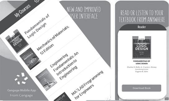
The Cengage Mobile App
Available on iOS and Android smartphones, the Cengage Mobile App provides convenience. Students can access their entire textbook anyplace and anytime. They can take notes, highlight important passages, and have their text read aloud whether they are online or off.
To download the mobile app, visit https://www.cengage.com/mobile-app/.
All-You-Can-Learn Access with Cengage Unlimited
Cengage Unlimited is the first-of-its-kind digital subscription that gives students total and on-demand access to all the digital learning platforms, eBooks, online homework, and study tools Cengage has to offer—in one place, for one price. With Cengage Unlimited, students get access to their WebAssign courseware, as well as content in other Cengage platforms and course areas from day one. That’s 70 disciplines and 675 courses worth of material, including engineering. With Cengage Unlimited, students get unlimited access to a library of more than 22,000 products. To learn more, visit https://www.cengage.com/unlimited.
About the Authors
Charles H. Roth, Jr. is Professor Emeritus of Electrical and Computer Engineering at the University of Texas at Austin. He has been on the UT faculty since 1961. He received his BSEE degree from the University of Minnesota, his MSEE and EE degrees from the Massachusetts Institute of Technology, and his PhD degree in EE from Stanford University. His teaching and research interests included logic design, digital systems design, switching theory, microprocessor systems, and computeraided design. He developed a self-paced course in logic design which formed the basis of his textbook, Fundamentals of Logic Design. He is also the author of Digital Systems Design Using VHDL, three other textbooks, and several software packages. He is the author or co-author of more than 50 technical papers and reports. Six PhD students and 80 MS students have received their degrees under his supervision. He received several teaching awards including the 1974 General Dynamics Award for Outstanding Engineering Teaching.
Larry L. Kinney is Professor Emeritus in Electrical and Computer Engineering at the University of Minnesota Twin Cities. He received his BS, MS, and PhD in Electrical Engineering from the University of Iowa in 1964, 1965, and 1968, respectively, and joined the University of Minnesota in 1968. He has taught a wide variety of courses including logic design, microprocessor/microcomputer systems, computer design, switching theory, communication systems and error-correcting codes. His major areas of research interest are testing of digital systems, built-in self-test, computer design, microprocessor-based systems, and error-correcting codes.
Eugene B. John is Professor of Electrical and Computer Engineering at the University of Texas at San Antonio. He received his PhD in Electrical Engineering from Pennsylvania State University. His teaching and research interests include Logic Design, Digital Systems Design, VLSI Design, Low Power VLSI Design, Computer Architecture, Energy Efficient Computing, Hardware for Machine Learning and Artificial Intelligence, and Hardware Security. He holds 3 U.S. patents and has published approximately 150 technical papers and reports. He has received several teaching awards including the University of Texas System Regents’ Outstanding Teaching Award (2014).
Introduction Number Systems and Conversion
Objectives
1. Introduction
The first part of this unit introduces the material to be studied later. In addition to getting an overview of the material in the first part of the course, you should be able to explain
a. The difference between analog and digital systems and why digital systems are capable of greater accuracy
b. The difference between combinational and sequential circuits
c. Why two-valued signals and binary numbers are commonly used in digital systems
2. Number systems and conversion
When you complete this unit, you should be able to solve the following types of problems:
a. Given a positive integer, fraction, or mixed number in any base (2 through 16); convert to any other base. Justify the procedure used by using a power series expansion for the number.
b. Add, subtract, multiply, and divide positive binary numbers. Explain the addition and subtraction process in terms of carries and borrows.
c. Write negative binary numbers in sign and magnitude, 1’s complement, and 2’s complement forms. Add signed binary numbers using 1’s complement and 2’s complement arithmetic. Justify the methods used. State when an overflow occurs.
d. Represent a decimal number in binary-coded-decimal (BCD), 6-3-1-1 code, excess-3 code, etc. Given a set of weights, construct a weighted code.
Study Guide
1. Study Section 1.1, Digital Systems and Switching Circuits, and answer the following study questions:
(a) What is the basic difference between analog and digital systems?
(b) Why are digital systems capable of greater accuracy than analog systems?
(c) Explain the difference between combinational and sequential switching circuits.
(d) What common characteristic do most switching devices used in digital systems have?
(e) Why are binary numbers used in digital systems?
2. Study Section 1.2, Number Systems and Conversion. Answer the following study questions as you go along:
(a) Is the first remainder obtained in the division method for base conversion the most or least significant digit?
(b) Work through all of the examples in the text as you encounter them and make sure that you understand all of the steps.
(c) An easy method for conversion between binary and hexadecimal is illustrated in Equation (1-1). Why should you start forming the groups of four bits at the binary point instead of the left end of the number?
(d) Why is it impossible to convert a decimal number to binary on a digit-by-digit basis as can be done for hexadecimal?
(e) Complete the following conversion table.
(f ) Work Problems 1.1, 1.2, 1.3, and 1.4.
3. Study Section 1.3, Binary Arithmetic.
(a) Make sure that you can follow all of the examples, especially the propagation of borrows in the subtraction process.
(b) To make sure that you understand the borrowing process, work out a detailed analysis in terms of powers of 2 for the following example:
4. Work Problems 1.5, 1.6, and 1.17(a).
5. Study Section 1.4, Representation of Negative Numbers.
(a) In digital systems, why are 1’s complement and 2’s complement commonly used to represent negative numbers instead of sign and magnitude?
(b) State two different ways of forming the 1’s complement of an n-bit binary number.
(c) State three different ways of forming the 2’s complement of an n-bit binary number.
(d) If the word length is n = 4 bits (including sign), what decimal number does 10002 represent in sign and magnitude? In 2’s complement? In 1’s complement?
(e) Given a negative number represented in 2’s complement, how do you find its magnitude?
Given a negative number represented in 1’s complement, how do you find its magnitude?
(f ) If the word length is 6 bits (including sign), what decimal number does 1000002 represent in sign and magnitude? In 2’s complement? In 1’s complement?
(g) What is meant by an overflow? How can you tell that an overflow has occurred when performing 1’s or 2’s complement addition?
Does a carry out of the last bit position indicate that an overflow has occurred?
(h) Work out some examples of 1’s and 2’s complement addition for various combinations of positive and negative numbers.
(i) What is the justification for using the end-around carry in 1’s complement addition?
(j) The one thing that causes the most trouble with 2’s complement numbers is the special case of the negative number which consists of a 1 followed by all 0’s (1000 . . . 000). If this number is n bits long, what number does it represent and why? (It is not negative zero.)
(k) Work Problems 1.7 and 1.8.
6. Study Section 1.5, Binary Codes.
(a) Represent 187 in BCD code, excess-3 code, 6-3-1-1 code, and 2-out-of-5 code.
(b) Verify that the 6-3-1-1 code is a weighted code. Note that for some decimal digits, two different code combinations could have been used. For example, either 0101 or 0110 could represent 4. In each case the combination with the smaller binary value has been used.
(c) How is the excess-3 code obtained?
(d) How are the ASCII codes for the decimal digits obtained? What is the relation between the ASCII codes for the capital letters and lowercase letters?
(e) Work Problem 1.9.
7. If you are taking this course on a self-paced basis, you will need to pass a readiness test on this unit before going on to the next unit. The purpose of the readiness test is to determine if you have mastered the material in this unit and are ready to go on to the next unit. Before you take the readiness test:
(a) Check your answers to the problems against those provided at the end of this book. If you missed any of the problems, make sure that you understand why your answer is wrong and correct your solution.
(b) Make sure that you can meet all of the objectives listed at the beginning of this unit.
Introduction Number Systems and Conversion
1.1 Digital Systems and Switching Circuits
Digital systems are used extensively in computation and data processing, control systems, communications, and measurement. Because digital systems are capable of greater accuracy and reliability than analog systems, many tasks formerly done by analog systems are now being performed digitally.
In a digital system, the physical quantities or signals can assume only discrete values, while in analog systems the physical quantities or signals may vary continuously over a specified range. For example, the output voltage of a digital system might be constrained to take on only two values such as 0 volts and 5 volts, while the output voltage from an analog system might be allowed to assume any value in the range 10 volts to +10 volts.
Because digital systems work with discrete quantities, in many cases they can be designed so that for a given input, the output is exactly correct. For example, if we multiply two 5-digit numbers using a digital multiplier, the 10-digit product will be correct in all 10 digits. On the other hand, the output of an analog multiplier might have an error ranging from a fraction of one percent to a few percent depending on the accuracy of the components used in construction of the multiplier. Furthermore, if we need a product which is correct to 20 digits rather than 10, we can redesign the digital multiplier to process more digits and add more digits to its input. A similar improvement in the accuracy of an analog multiplier would not be possible because of limitations on the accuracy of the components.
The design of digital systems may be divided roughly into three parts—system design, logic design, and circuit design. System design involves breaking the overall system into subsystems and specifying the characteristics of each subsystem. For example, the system design of a digital computer could involve specifying the number and type of memory units, arithmetic units, and input-output devices as well as the interconnection and control of these subsystems. Logic design involves determining how to interconnect basic logic building blocks to perform a specific function. An example of logic design is determining the interconnection of logic gates and flip-flops required to perform binary addition. Circuit design involves specifying the interconnection of specific components such as resistors, diodes, and transistors
FIgUre 1-1
Switching Circuit
Cengage Learning 2014
to form a gate, flip-flop, or other logic building block. Most contemporary circuit design is done in integrated circuit form using appropriate computer-aided design tools to lay out and interconnect the components on a chip of silicon. This book is largely devoted to a study of logic design and the theory necessary for understanding the logic design process. Some aspects of system design are treated in Units 18 and 20. Circuit design of logic gates is discussed briefly in Appendix A.
Many of a digital system’s subsystems take the form of a switching circuit (Figure 1-1). A switching circuit has one or more inputs and one or more outputs which take on discrete values. In this text, we will study two types of switching circuits—combinational and sequential. In a combinational circuit, the output values depend only on the present value of the inputs and not on past values. In a sequential circuit, the outputs depend on both the present and past input values. In other words, in order to determine the output of a sequential circuit, a sequence of input values must be specified. The sequential circuit is said to have memory because it must “remember” something about the past sequence of inputs, while a combinational circuit has no memory. In general, a sequential circuit is composed of a combinational circuit with added memory elements. Combinational circuits are easier to design than sequential circuits and will be studied first.
The basic building blocks used to construct combinational circuits are logic gates. The logic designer must determine how to interconnect these gates in order to convert the circuit input signals into the desired output signals. The relationship between these input and output signals can be described mathematically using Boolean algebra. Units 2 and 3 of this text introduce the basic laws and theorems of Boolean algebra and show how they can be used to describe the behavior of circuits of logic gates.
Starting from a given problem statement, the first step in designing a combinational logic circuit is to derive a table or the algebraic logic equations which describe the circuit outputs as a function of the circuit inputs (Unit 4). In order to design an economical circuit to realize these output functions, the logic equations which describe the circuit outputs generally must be simplified. Algebraic methods for this simplification are described in Unit 3, and other simplification methods (Karnaugh map and Quine-McCluskey procedure) are introduced in Units 5 and 6. Implementation of the simplified logic equations using several types of gates is described in Unit 7, and alternative design procedures using programmable logic devices are developed in Unit 9.
The basic memory elements used in the design of sequential circuits are called flip-flops (Unit 11). These flip-flops can be interconnected with gates to form counters and registers (Unit 12). Analysis of more general sequential circuits using timing
diagrams, state tables, and graphs is presented in Unit 13. The first step in designing a sequential switching circuit is to construct a state table or graph which describes the relationship between the input and output sequences (Unit 14). Methods for going from a state table or graph to a circuit of gates and flip-flops are developed in Unit 15. Methods of implementing sequential circuits using programmable logic are discussed in Unit 16. In Unit 18, combinational and sequential design techniques are applied to the realization of systems for performing binary addition, multiplication, and division. The sequential circuits designed in this text are called synchronous sequential circuits because they use a common timing signal, called a clock, to synchronize the operation of the memory elements.
Use of a hardware description language, VHDL, in the design of combinational logic, sequential logic, and digital systems is introduced in Units 10, 17, and 20. VHDL is used to describe, simulate, and synthesize digital hardware. After writing VHDL code, the designer can use computer-aided design software to compile the hardware description and complete the design of the digital logic. This allows the completion of complex designs without having to manually work out detailed circuit descriptions in terms of gates and flip-flops.
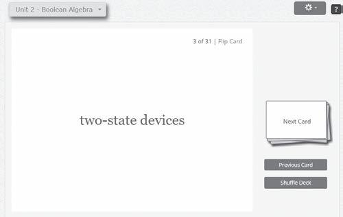
The switching devices used in digital systems are generally two-state devices, that is, the output can assume only two different discrete values. Examples of switching devices are relays, diodes, and transistors. A relay can assume two states—closed or open—depending on whether power is applied to the coil or not. A diode can be in a conducting state or a nonconducting state. A transistor can be in a cut-off or saturated state with a corresponding high or low output voltage. Of course, transistors can also be operated as linear amplifiers with a continuous range of output voltages, but in digital applications greater reliability is obtained by operating them as twostate devices. Because the outputs of most switching devices assume only two different values, it is natural to use binary numbers internally in digital systems. For this reason binary numbers and number systems will be discussed first before proceeding to the design of switching circuits.
1.2 Number Systems and Conversion
When we write decimal (base 10) numbers, we use a positional notation; each digit is multiplied by an appropriate power of 10 depending on its position in the number. For example,
Similarly, for binary (base 2) numbers, each binary digit is multiplied by the appropriate power of 2:
Note that the binary point separates the positive and negative powers of 2 just as the decimal point separates the positive and negative powers of 10 for decimal numbers.
Any positive integer R (R > 1) can be chosen as the radix or base of a number system. If the base is R, then R digits (0, 1, . . . , R 1) are used. For example, if R = 8, then the required digits are 0, 1, 2, 3, 4, 5, 6, and 7. A number written in positional notation can be expanded in a power series in R. For example,
where ai is the coefficient of Ri and 0 ≤ ai ≤ R 1. If the arithmetic indicated in the power series expansion is done in base 10, then the result is the decimal equivalent of N . For example,
The power series expansion can be used to convert to any base. For example, converting 14710 to base 3 would be written as
where all the numbers on the right-hand side are base 3 numbers. (Note: In base 3, 10 is 101, 7 is 21, etc.) To complete the conversion, base 3 arithmetic would be used. Of course, this is not very convenient if the arithmetic is being done by hand. Similarly, if 14710 is being converted to binary, the calculation would be
Again this is not convenient for hand calculation but it could be done easily in a computer where the arithmetic is done in binary. For hand calculation, use the power series expansion when converting from some base into base 10. For bases greater than 10, more than 10 symbols are needed to represent the digits. In this case, letters are usually used to represent digits greater than 9. For example, in hexadecimal (base 16), A represents 1010, B represents 1110, C represents 1210, D represents 1310, E represents 1410, and F represents 1510. Thus,
Next, we will discuss conversion of a decimal integer to base R using the division method. The base R equivalent of a decimal integer N can be represented as