OxideElectronics
Editedby AsimRay
BrunelUniversity London,UK
Thiseditionfirstpublished2021
©2021JohnWileyandSonsLtd
Allrightsreserved.Nopartofthispublicationmaybereproduced,storedinaretrievalsystem,ortransmitted,in anyformorbyanymeans,electronic,mechanical,photocopying,recordingorotherwise,exceptaspermittedby law.Adviceonhowtoobtainpermissiontoreusematerialfromthistitleisavailableathttp://www.wiley.com/go/ permissions.
TherightofAsimRaytobeidentifiedasauthoroftheeditorialmaterialinthisworkhasbeenassertedin accordancewithlaw.
RegisteredOffices
JohnWiley&Sons,Inc.,111RiverStreet,Hoboken,NJ07030,USA
JohnWiley&SonsLtd,TheAtrium,SouthernGate,Chichester,WestSussex,PO198SQ,UK
EditorialOffice
TheAtrium,SouthernGate,Chichester,WestSussex,PO198SQ,UK
Fordetailsofourglobaleditorialoffices,customerservices,andmoreinformationaboutWileyproductsvisitusat www.wiley.com.
Wileyalsopublishesitsbooksinavarietyofelectronicformatsandbyprint-on-demand.Somecontentthat appearsinstandardprintversionsofthisbookmaynotbeavailableinotherformats.
LimitofLiability/DisclaimerofWarranty
Inviewofongoingresearch,equipmentmodifications,changesingovernmentalregulations,andtheconstantflow ofinformationrelatingtotheuseofexperimentalreagents,equipment,anddevices,thereaderisurgedtoreview andevaluatetheinformationprovidedinthepackageinsertorinstructionsforeachchemical,pieceofequipment, reagent,ordevicefor,amongotherthings,anychangesintheinstructionsorindicationofusageandforadded warningsandprecautions.Whilethepublisherandauthorshaveusedtheirbesteffortsinpreparingthiswork,they makenorepresentationsorwarrantieswithrespecttotheaccuracyorcompletenessofthecontentsofthiswork andspecificallydisclaimallwarranties,includingwithoutlimitationanyimpliedwarrantiesofmerchantabilityor fitnessforaparticularpurpose.Nowarrantymaybecreatedorextendedbysalesrepresentatives,writtensales materialsorpromotionalstatementsforthiswork.Thefactthatanorganization,website,orproductisreferredto inthisworkasacitationand/orpotentialsourceoffurtherinformationdoesnotmeanthatthepublisherand authorsendorsetheinformationorservicestheorganization,website,orproductmayprovideorrecommendations itmaymake.Thisworkissoldwiththeunderstandingthatthepublisherisnotengagedinrenderingprofessional services.Theadviceandstrategiescontainedhereinmaynotbesuitableforyoursituation.Youshouldconsultwith aspecialistwhereappropriate.Further,readersshouldbeawarethatwebsiteslistedinthisworkmayhavechanged ordisappearedbetweenwhenthisworkwaswrittenandwhenitisread.Neitherthepublishernorauthorsshallbe liableforanylossofprofitoranyothercommercialdamages,includingbutnotlimitedtospecial,incidental, consequential,orotherdamages.
LibraryofCongressCataloging-in-PublicationData
Names:Ray,AsimK.,editor.
Title:Oxideelectronics/editedbyAsimRay,BrunelUniversity London,England,UnitedKingdom.
Description:Firstedition.|Hoboken,NJ,USA:JohnWileyandSons,Inc., 2021.|Series:Wileyseriesinmaterialsforelectronic& optoelectronicapplications|Includesbibliographicalreferencesand index.
Identifiers:LCCN2020051123(print)|LCCN2020051124(ebook)|ISBN 9781119529477(hardback)|ISBN9781119529484(adobepdf)|ISBN 9781119529507(epub)
Subjects:LCSH:Electronics–Materials.|Metallicoxides.| Oxides–Electricproperties.
Classification:LCCTK7871.O952021(print)|LCCTK7871(ebook)|DDC 621.381028/4–dc23
LCrecordavailableathttps://lccn.loc.gov/2020051123
LCebookrecordavailableathttps://lccn.loc.gov/2020051124
CoverDesign:Wiley
CoverImages:CourtesyofSubhasishBasuMajumder Setin10/12ptWarnockProbySPiGlobal,Chennai,India 10987654321
Contents
SeriesPreface xiii
Preface xv
ListofContributors xvii
1GrapheneOxideforElectronics1 FenghuaLiu,LifengZhang,LijianWang,BinyuanZhaoandWeipingWu
1.1Introduction1
1.2SynthesisandCharacterizationsofGrapheneOxide2
1.2.1ChemicalReductionofGrapheneOxide(GO)2
1.2.2MicrowaveMethod2
1.2.3PlasmaMethod3
1.2.4LaserMethod4
1.3EnergyHarvestApplicationsofGrapheneOxide5
1.3.1SolarCells5
1.3.2SolarThermalEnergyHarvestDevices7
1.4EnergyStorageApplicationsofGrapheneOxide7
1.4.1Supercapacitors7
1.4.2Batteries10
1.5ElectronicDeviceApplicationsofGrapheneOxide12
1.6LargeAreaElectronicsApplicationsofGrapheneOxide13 References16
2FlexibleandWearableGraphene-BasedE-Textiles21 NazmulKarim,ShailaAfroj,DamienLeechandAmrM.Abdelkader
2.1IntroductiontoWearableE-Textiles21
2.2SynthesisofGrapheneDerivatives22
2.2.1GrapheneOxide22
2.2.2ReducedGrapheneOxide24
2.3Graphene-BasedWearableE-Textiles25
2.3.1Graphene-BasedTextileFibres26
2.3.2Graphene-CoatedTextiles27
2.3.3Graphene-PrintedWearableE-Textiles28
2.3.3.1ScreenPrinting30
2.3.3.2InkjetPrinting30
2.4SurfacePre-andPost-TreatmentofSubstrates32
2.5Applications34
2.5.1Sensors34
2.5.2Supercapacitor36
2.5.3RechargeableBatteries38
2.5.4Optoelectronics39 2.6ChallengesandOutlook40 References41
3MagneticInteractionsintheCubicMottInsulatorsNiO,MnO,andCoOandthe RelatedOxidesCuOandFeO51 DavidJ.LockwoodandMichaelG.Cottam
3.1Introduction51
3.2Spin–SpinInteractions52
3.2.1MagneticOrderingBelow T N 52
3.2.2Magnetostriction53
3.2.3MagneticandElectronicExcitations54
3.3Spin–PhononInteractions59
3.3.1PhononandMagnonTemperatureDependences60
3.3.2PhononModeSplittingBelow T N 62
3.4OtherRelatedMaterials64
3.4.1CupricOxide64
3.4.2IronMonoxide65
3.5Conclusions68 Acknowledgments68 References68
4High-�� DielectricOxidesforElectronics75 TongZhang,XiaoyangZhang,YiYangandWeipingWu
4.1IntroductionofHigh-�� DielectricOxides75
4.1.1GroupIIIADielectricOxides77
4.1.2GroupIIIBHigh-�� DielectricOxides77
4.1.3GroupIVBHigh-�� DielectricOxides77
4.2TheDepositionofHigh-�� OxideDielectrics78
4.3High-�� DielectricOxidesforField-EffectTransistors80
4.3.1High-�� DielectricOxidesfortheMOSFETs80
4.3.2High-�� DielectricOxidesforTunnelField-EffectTransistors84
4.4High-�� DielectricOxidesforMemoryDevices85
4.4.1High-�� DielectricOxidesforDRAM85
4.4.2High-�� DielectricOxidesforReRAM87 References88
5LowTemperatureGrowthofGermaniumOxideNanowiresbyTemplateBased SelfAssemblyandtheirRamanCharacterization93 RaisaFabiha,AbigailCasey,GregoryTriplettandSupriyoBandyopadhyay 5.1Introduction93
5.2Synthesis93 5.3Characterization96 5.4RamanMeasurements96 5.5Conclusion98 References99
6ElectronicPhenomena,Electroforming,ResistiveSwitching,andDefect ConductionBandsinMetal-Insulator-MetalDiodes101 ThomasW.Hickmott
6.1Introduction101
6.2Experimental103
6.3Electroforming,Electroluminescence,andElectronEmission104
6.3.1ElectroformingofAl-Al2 O3 -AgDiodes104
6.3.2ElectroluminescencefromAl-Al2 O3 -AgDiodes104
6.3.3ElectronEmissionfromAl-Al2 O3 -AgDiodes105
6.3.4VCNR,EL,andEMinOtherInsulators107
6.3.5TemperatureDependenceofEM108
6.4ElectrodeEffectsinResistiveSwitchingofNb-Nb2 O5 -MetalDiodes109
6.4.1ResistiveSwitchinginNb-Nb2 O5 -MetalDiodes109
6.4.2ResistiveSwitchingatLowTemperatures109
6.4.3Structurein I-V CurvesofElectroformedNb-Nb2 O5 -Metal Diodes110
6.5Conduction,Electroluminescence,andPhotoconductivityBefore ElectroformingMIMDiodes112
6.5.1ConductioninNb-Nb2 O5 -AuDiodes112
6.5.2ElectroluminescenceinNb-Nb2 O5 -AuDiodes112
6.5.3ConductionandElectroluminescenceinMIMDiodeswith TiO2 andTa2 O5 115
6.5.4PhotoconductivityinMIMDiodes115 6.6Discussion118
6.6.1DefectConductionBandsinAmorphousAl2 O3 119
6.6.2DefectConductionBandsinAmorphousNb2 O5 121
6.6.3DefectConductionBandsinAmorphousInsulators123
6.7SummaryandConclusions125 References125
7LeadOxideasMaterialofChoiceforDirectConversionDetectors129 AllaReznikandOleksiiSemeniuk
7.1Introduction129
7.2CrystalStructureandElectronicPropertiesofPbO130
7.2.1CrystalStructureofTetragonalPbO(�� -PbO)131
7.2.2CrystalStructureofOrthorhombicPbO(�� -PbO)132
7.2.3ElectronicPropertiesof �� -and �� -PbO133
7.3DepositionProcessofPbOLayers135
7.4ChargeTransportMechanisminLeadOxide147
7.4.1ElectronTransportinpoly-PbO148 References151
8ZnOVaristors:FromGrainBoundariestoPowerApplications157 FelixGreuter
8.1Introduction157
8.2ManufacturingProcessofZnOVaristors160
8.3MicrostructureandGrainBoundaries162
8.4GrainBoundaryPotentialBarriers168
8.5The‘DoubleSchottkyBarrierDefectModel’174
8.6HotElectronEffectsControllingtheBreakdownRegion181
8.7HotElectronEffectsandDynamicResponse185
8.8FromSingleGrainBoundariestoMicrostructuresandVaristorDevices196
8.9AgeingandLong-TermStabilityofVaristorMaterials207
8.10EnergyAbsorptionCapabilityandHighCurrentImpulseStresses218
8.11SummaryandOutlook223 Acknowledgements226 References226
9FundamentalPropertiesandPowerElectronicDeviceProgressofGallium Oxide 235 XuanhuChen,ChennupatiJagadishandJiandongYe 9.1Introduction235
9.2ElectronicPropertiesandDefectsofGa2 O3 236
9.2.1BulkCrystals,Epitaxy,andn–typeDoping237
9.2.2ElectronicBandStructureandFeasibilityofp–typeDoping240
9.2.3DefectBehaviourinBulkCrystalsandEpitaxialFilms245
9.3BasicDeviceCharacteristics250
9.3.1Metal-SemiconductorContact250
9.3.1.1BarrierFormation250
9.3.1.2Image-ForceLowering252
9.3.1.3CarrierTransportandBreakdown254
9.3.2PhysicsofDeepDepletionGa2 O3 MOSFETs257
9.3.2.1Metal-Insulator-SemiconductorCapacitors257
9.3.2.2BasicDeviceCharacteristicsofDepletionMode MOSFETsBasedonGa2 O3 270
9.3.2.3ApproachestoEnhancement-Mode �� -Ga2 O3 MOSFETs280
9.3.3RelevantFigureofMeritinGa2 O3 282
9.4Ga2 O3 SchottkyRectifiers286
9.4.1EdgeTerminations287
9.4.2Ga2 O3 SchottkyRectifiers295
9.4.3Ga2 O3 p-nHeterojunctionDiodes301
9.5Ga2 O3 Transistors307
9.5.1OhmicContactstoGa2 O3 307
9.5.2DielectricMaterialsforGa2 O3 andMOSCaps308
9.5.3LateralGa2 O3 FETs313
9.5.4 �� -Ga2 O3 MODFETs324
9.5.5VerticalGa2 O3 MOSFETs330 9.6Summary335 References336
10EmergingTrends,Challenges,andApplicationsinSolid-StateLaserCooling353 JyothisThomas,LauroMaia,YannickLedemi,YounesMessaddeqandRaman Kashyap 10.1Introduction353 10.2Theory355
10.3ExperimentalDesignConsiderationsforCooling357
10.3.1ExperimentalSetupsUsedforSolid-stateLaserCooling357
10.3.1.1Crystals357
10.3.1.2Glasses358
10.3.1.3SilicaGlassOpticalFibres360
10.3.1.4SemiconductorNanoribbons361
10.3.2TechniquestoAnalyseBackgroundAbsorption(�� b )Coefficient361
10.3.3TemperatureMeasurementTechniquesinSolid-StateLaser Cooling362
10.3.3.1ThermalImaging362
10.3.3.2Photoluminescence(PL)Thermometry363
10.3.3.3TemperatureMeasurementUsingFibreBragg Gratings363
10.3.3.4Thermocouples364
10.3.3.5PhotothermalDeflectionSpectroscopy(PTDS)364
10.3.3.6InterferometricTechnique364
10.4LaserCoolingMaterialsandProperties365
10.4.1Crystals366
10.4.2Semiconductors368
10.4.3OpticalFibres370
10.4.4NanocrystallinePowders371
10.5OxyfluorideGlass-Ceramics:RecentDevelopmentsinSolid-State LaserCooling373
10.5.1Earth-DopedOxyfluoridePseudo-BinaryGlassesand Glass-CeramicsforOpticalRefrigeration375 10.5.1.1MaterialsandMethods376 10.5.1.2ResultsandDiscussion376 10.5.1.3SummaryonPseudo-BinaryOxyfluorideGlass Ceramics381 10.6OpticalCryocoolerDevices382 10.7FutureProspectsandConclusions386 Acknowledgements388 References388
11ElectrodeMaterialsforSodiumIonRechargeableBatteries397 TaniaMajumder,AnwesaMukherjee,DebasishDasandS.B.Majumder 11.1Introduction–ReviewoftheConstituentsUsedinNa–IonCells397 11.2CathodeMaterialsforNaIonRechargeableCells397 11.2.1TransitionMetalOxideswithLayeredStructure397 11.2.2PrussianBlueAnalogue398 11.2.3SodiumSuperionicConductors(NASICON)399 11.2.4OtherCathodes400 11.3CurrentCollectors,Binder,andElectrolyte400 11.4AnodeMaterialsforNaIonRechargeableCells401 11.4.1CarbonaceousMaterials401 11.4.2AlloyingTypeAnodes401 11.4.3ConversionTypeAnodes402 11.4.4OtherAnodes402
11.5OutstandingResearchIssuesandStatementoftheProblem402
11.6SynthesisandElectrochemicalCharacterizationofElectrodes404
11.6.1IlmeniteNiTiO3 asAnode404
11.6.1.1SynthesisandCharacterization404
11.6.2ElectrochemicalCharacterization404
11.6.3ElectrophoreticDepositionofNiTiO3 -BasedAnode406
11.6.4ElectrochemicalPerformanceofEPDGrownNTOAnodes408
11.7Na2 Ti3 O7 asAnode409
11.7.1SynthesisandCharacterization409
11.7.2ElectrochemicalCharacterizationofPristineNaTO410
11.7.3ElectrochemicalPerformanceofCarbon-CoatedNaTOAnode411
11.7.4ElectrochemicalPerformanceofNaTO/rGOCompositeAnode413 11.8PBAasCathode414
11.8.1NickelHexacyanoferrate(NiHCF)415
11.8.2IronHexacyanoferrate(FeHCF)417 11.9SummaryandConclusions418 Acknowledgement419 References419
12PerovskitesforPhotovoltaics423 HoomanMehdizadehRad,DavidOmpongandJaiSingh 12.1Introduction423 12.2DiffusionLength424
12.2.1Methodology425
12.2.2ResultsofSimulatedDiffusionLengthandDiscussions427 12.3Open-CircuitVoltage432
12.3.1ResultsofOpen-CircuitVoltageandDiscussions433
12.3.2BimolecularRecombination436 12.4InfluenceofDensityofTailStatesatInterfaces437 12.4.1Methods437
12.4.2ResultsofDensityofStatesandDiscussions441 12.5Conclusions444 References447
13AdvancedCharacterizationsofOxidesforOptoelectronicApplications453 U.Onwukwe,L.AnguilanoandP.Sermon
13.1ABriefHistoryofOptoelectronicDevices453
13.1.1Semiconductors454
13.1.1.1n-TypeExtrinsicSemiconductors455
13.1.1.2p-TypeExtrinsicSemiconductors456
13.2InteractionofSemiconductorsandtheOptoelectronicPhenomenon457
13.2.1DirectBandGapSemiconductors457
13.2.1.1IndirectBandGapSemiconductors458
13.2.2OxidesforOptoelectronics:Introduction459
13.2.3MajorTypesofMOforOptoelectronics460
13.2.3.1ITO460
13.2.3.2ZnO460
13.2.3.3AZO461
13.2.3.4IGZO461
13.2.3.5PerovskiteOxides462
13.2.3.6ReducedGrapheneOxide-MiscellaneousMaterials463
13.2.4MethodofPreparationofOptoelectronicStructures467
13.2.4.1Nanowires/Nanorods467
13.2.4.2ThinFilms467
13.2.4.3MixedMorphologiesFabrication468
13.3CharacterizationTechniquesandtheirUseforMetalOxide Optoelectronics470
13.3.1RutherfordBackscatteringSpectrometry(RBS)470
13.3.2Fourier-TransformInfra-Red(FTIR)471
13.3.2.1RamanSpectroscopy473
13.3.3ScanningElectronMicroscopy(SEM)475
13.3.4TransmissionElectronMicroscope(TEM)477
13.3.5LuminescenceTechniques480
13.3.6X-RayDiffraction482
13.4FacilitiesandCaseStudies484
13.4.1CaseStudyI–LeafBiotemplateDerivedTiO2 485 References488
14FutureTuningOptoelectronicOxidesfromtheInside:Sol-Gel(TiO2 )x -(SiO2 )100-x 497
M.P.Worsley,J.G.Leadley,R.M.A.MacGibbon,T.Salvesen,P.A.SermonandJ.M. Charnock
14.1IntroductionandBackground497
14.1.1PhotonsandWavetrains497
14.1.2OptoelectronicOxidesandDevices497
14.1.5AlkoxideandSol-GelRoutestoTiO2 -SiO2
14.1.6Miscibilityandthe%TiO2 (x)AddedinTiO2 -SiO2
14.1.7DopingofTiO2 -SiO2
14.1.8LocalStructureinTiO2 -SiO2
14.2Hypothesis503 14.3Experimental504
14.3.1Materials504
14.3.2Preparations504
14.3.3CharacterizationMethods504
14.4CharacterizationResults505
14.5DiscussiononFutureAutomatedCALPHADDesign,Dip-Coating Mechanical,andHigh-ThroughputScreeningofNovelOptoelectronic OxidesandDevices510
14.6ConclusionsonTiO2 -SiO2 Use510 Acknowledgements513 References513
15BinaryCalcia-AluminaThinFilms:SynthesisandPropertiesandApplications525 AsimK.Ray
15.1Introduction525
15.2StructuralandPhysicalPropertiesofC12A7526
15.2.1ThermalStability528
15.2.2IonicConductivityandMechanismsofOxide–IonMigration529
15.3AtomicandElectronicStructure530
15.3.1SynthesisofC12A7531
15.3.2SinglePowders531
15.3.3SingleCrystal532
15.3.4PolycrystallineBulk533
15.3.5ThinFilm535
15.3.6IonDopinginC12A7536
15.3.6.1HeatTreatmentinH2 Atmosphere537
15.3.6.2Thermoelectricity537
15.4OpticalProperties540
15.4.1Reflectivity541
15.4.2Luminescence542
15.5ApplicationsofC12A7543
15.6Summary545 Acknowledgements546 References546
16OxideCathodes553 IanAlberts
16.1HistoricalAspects553
16.1.1TheEdisonEffect555
16.1.2ArthurWehnelt555
16.1.3ThermionicEmissionResearchintheEarlyTwentiethCentury556
16.1.4OxideCathodesfortheCRT556
16.2PhysicsofThermionicEmission557
16.2.1DerivationoftheRichardson-DushmanEquation558
16.2.2SpaceChargeandtheChild-LangmuirLaw559
16.3OxideCathodeDevelopment560
16.3.1TheBarium-CoatedCathode561
16.3.2TheRiseandSubsequentFalloftheImpregnatedCathode562
16.3.3CermetCathodes565
16.3.4StateoftheArt565
16.4FutureTrendsandOngoingApplications567
16.4.1VacuumX-RayTubes568
16.4.2MilitaryTelecommunications568
16.4.3Klystrons570
16.4.4Gyrotron571
16.4.5ThermionicEnergyConversion571
16.4.6TriboelectricNanogenerators573
16.4.7FrontiersinThermionicResearch:VacuumNanoelectronics575
16.4.8FieldEmissionDisplays(FED)575 16.5Conclusion577 References577 Index 583
SeriesPreface
WileySeriesinMaterialsforElectronicandOptoelectronic Applications
Thisbookseriesisdevotedtotherapidlydevelopingclassofmaterialsusedforelectronicandoptoelectronicapplications.Itisdesignedtoprovidemuch-neededinformationonthefundamentalscientificprinciplesofthesematerials,togetherwithhow theseareemployedintechnologicalapplications.Thebooksareaimedat(postgraduate)students,researchers,andtechnologists,engagedinresearch,development,andthe studyofmaterialsinelectronicsandphotonics,andindustrialscientistsdevelopingnew materials,devices,andcircuitsfortheelectronic,optoelectronicand,communications industries.
Thedevelopmentofnewelectronicandoptoelectronicmaterialsdependsnotonlyon materialsengineeringatapracticallevel,butalsoonaclearunderstandingofthepropertiesofmaterials,andthefundamentalsciencebehindtheseproperties.Itisthepropertiesofamaterialthateventuallydetermineitsusefulnessinanapplication.Theseries thereforealsoincludessuchtitlesaselectricalconductioninsolids,opticalproperties, thermalproperties,andsoon,allwithapplicationsandexamplesofmaterialsinelectronicsandoptoelectronics.Thecharacterizationofmaterialsisalsocoveredwithinthe seriesinasmuchasitisimpossibletodevelopnewmaterialswithoutthepropercharacterizationoftheirstructureandproperties.Structure–propertyrelationshipshave alwaysbeenfundamentallyandintrinsicallyimportanttomaterialsscienceandengineering.
Materialsscienceiswellknownforbeingoneofthemostinterdisciplinarysciences. Itistheinterdisciplinaryaspectofmaterialssciencethathasledtomanyexcitingdiscoveries,newmaterialsandnewapplications.Itisnotunusualtofindscientistswith achemicalengineeringbackgroundworkingonmaterialsprojectswithapplicationsin electronics.Inselectingtitlesfortheseries,wehavetriedtomaintaintheinterdisciplinaryaspectofthefield,andhenceitsexcitementtoresearchersinthisfield.
ArthurWilloughby PeterCapper SafaKasap
Preface
Potentialapplicationsofoxideelectronicmaterialsarevast.Transparentelectronics, optoelectronics,magnetoelectronic,photonics,spintronics,thermoelectric,piezoelectric,resistiveswitching,powerharvesting,hydrogenstorage,andenvironmentalwaste managementhasstimulatedhugeinterests,bothacademicandindustrial,inoxideelectronics.Thevastwealthoffunctionalpropertiesofoxidesisfirstrootedintheextreme diversityofcharacterizingtechniques.Complextransitionmetaloxidesexhibitmanifoldphysicalpropertiescomprisinghigh-temperaturesuperconductivity,piezoelectricity,ferroelectricity,magnetism,multiferroicity,andresistiveswitching.Thefunctional propertiesofcomplexmetaloxidesareverysensitivetothedetailsofelectronicstructureandaretherebystronglyinfluencedbytheelementalcompositionandthepresence ofdefectsorlatticedistortions.Thenanoscaleformofoxidesprovidesanewdimension duetotheincreasedsurface-to-volumeratio.
Thishandbookcontains16chapters.Thesetopicshaveabroaderappealwithaview tosatisfyingthemultidisciplinaryneedofelectricalandelectronicengineers,physicists,andmaterialscientists.Theformatofthesechaptersissimilartooneanother. Forexample,eachbeginswithanabstractfollowedbyanintroductiontothetopic andaclearillustrationofcontentswithrelevantequationsandgraphicalillustrations. Chaptersendwithasummaryofthedescription.Eachchaptercontainsanadequate numberofsupportingreferences,pointingouttheadditionalcontributiontoexisting knowledge.Allchaptersareself-containedwithnooverlappingintheircontents.Difficultmathematicshasbeenavoidedasfaraspossibleindescribingthesciencewithin thechapters.Thehandbookishighlyinterdisciplinarysothatitschaptersarevaluable forreaderswithdifferentbackgrounds.
Iamverygratefultoalltheauthorsfortheirexcellentcontributions.Eachtopic ismultidisciplinary,Therefore,readerswithchemistrybackgroundsbutworkingin electricalengineeringwillmaybeinterestedinthishandbook.Similarly,physicists willbenefitfromthishandbookinordertoacquireknowledgeinmaterialsscience. Theauthors’cooperationindeliveringtheirmanuscriptsduringdifferentstagesof productionhasalsobeenverymuchappreciated.SincerethanksareduetoJenny CosshamandKatrinaMacedafortheirhelpoverseveralmonthsincommissioningthe contributionsandgettingthemreadyforproduction.
xvi Preface
ItismygreatpleasuretothankProfessorSafaKasapforhismanyhelpfulsuggestions. HeistheEditor-in-Chiefof MaterialsScience:MaterialsinElectronics.Hisadviceon theselectionofchaptersandtheirauthorshasbeenverymuchappreciated. Finally,theeditorwishestothankallthemembersoftheirfamily(Arunima,Raj, Madhurima,Rishabh,MayanandReuben).
AsimRay London,UK,August2016
ListofContributors
AmrM.Abdelkader DepartmentofDesignandEngineering BournemouthUniversity Dorset UK
ShailaAfroj CentreforFinePrintResearch TheUniversityofWestofEngland Bristol UK
U.Onwukwe,L.Anguilano CollegeofEngineering, DesignandPhysicalSciences BrunelUniversityLondon Uxbridge UK
IanAlberts DepartmentofNuclearMedicine Inselspital,BernUniversityHospital UniversityofBern Bern Switzerland and
LG.PhilipsDisplays Lancashire UK
SupriyoBandyopadhyay DepartmentofElectricalandComputer Engineering
VirginiaCommonwealthUniversity Richmond USA
AbigailCasey DepartmentofElectricalandComputer Engineering
VirginiaCommonwealthUniversity Richmond USA
J.M.Charnock NanomaterialsandApplications Laboratory CEDPS,BraggBuilding BrunelUniversity Uxbridge UK
XuanhuChen SchoolofElectronicScienceand Engineering NanjingUniversity Nanjing China
MichaelG.Cottam DepartmentofPhysicsandAstronomy WesternUniversity,London Ontario Canada
DebasishDas SchoolofNanoScienceandTechnology IndianInstituteofTechnology Kharagpur W.Bengal India
RaisaFabiha DepartmentofElectricalandComputer Engineering
VirginiaCommonwealthUniversity Richmond USA
FelixGreuter DepartmentofEnergy&Materials ABBCorporateResearch Baden-Daettwil Switzerland
ThomasW.Hickmott DepartmentofPhysics StateUniversityofNewYorkatAlbany Albany USA
ChennupatiJagadish DepartmentofElectronicMaterials EngineeringandARCCentreof ExcellenceonTransformative Meta-OpticalSystems ResearchSchoolofPhysics AustralianNationalUniversity,ACT Canberra Australia
NazmulKarim CentreforFinePrintResearch TheUniversityofWestofEngland Bristol UK
RamanKashyap DepartmentofEngineeringPhysics ÉcolePolytechniquedeMontréal Canada
J.G.Leadley NanomaterialsandApplications Laboratory
CEDPS,BraggBuilding BrunelUniversity Uxbridge UK
YannickLedemi DepartmentofElectricalEngineering ÉcolePolytechniquedeMontréal Canada
DamienLeech CentreforFinePrintResearch
TheUniversityofWestofEngland Bristol UK
FenghuaLiu ShanghaiInstituteofOpticsandFine Mechanics ChineseAcademyofSciences Shanghai China
DavidJ.Lockwood MetrologyResearchCentre NationalResearchCouncilCanada Ottawa,Ontario Canada
R.M.A.MacGibbon NanomaterialsandApplications Laboratory
CEDPS,BraggBuilding BrunelUniversity Uxbridge UK
LauroMaia InstitutodeFísica UniversidadeFederaldeGoiás Goiânia Brazil
S.B.Majumder MaterialsScienceCentre IndianInstituteofTechnology
Kharagpur
W.Bengal
India
TaniaMajumder MaterialsScienceCentre
IndianInstituteofTechnology
Kharagpur W.Bengal
India
HoomanMehdizadehRad CollegeofEngineering ITandEnvironment
CharlesDarwinUniversity
Darwin Australia
YounesMessaddeq Centred′ optique, PhotoniqueetLaser UniversitéLaval
Québec
Canada
AnwesaMukherjee MaterialsScienceCentre
IndianInstituteofTechnology
Kharagpur
W.Bengal
India
DavidOmpong CollegeofEngineering ITandEnvironment
CharlesDarwinUniversity
Darwin Australia
AsimK.Ray Design&PhysicalSciences CollegeofEngineering BrunelUniversity Uxbridge UK
AllaRez PhysicsDepartment LakeheadUniversity ThunderBay Canada and ThunderBayRegionalHealthResearch Institute ThunderBay Canada
T.Salvesen NanomaterialsandApplications Laboratory CEDPS,BraggBuilding BrunelUniversity Uxbridge UK
OleksiiSemeniuk RadiationMedicineProgram PrincessMargaretCancerCentre Toronto,ON Canada
JaiSingh CollegeofEngineering ITandEnvironment CharlesDarwinUniversity
Darwin Australia
P.Sermon CollegeofEngineering, DesignandPhysicalSciences BrunelUniversityLondon Uxbridge UK
xx ListofContributors
JyothisThomas
DepartmentofEngineeringPhysics ÉcolePolytechniquedeMontréal Canada
GregoryTriplett
DepartmentofElectricalandComputer Engineering
VirginiaCommonwealthUniversity Richmond USA
LijianWang SchoolofMaterialsScienceand Engineering
ShanghaiJiaoTongUniversity Shanghai China
M.P.Worsley NanomaterialsandApplications Laboratory CEDPS,BraggBuilding BrunelUniversity Uxbridge UK
WeipingWu
ShanghaiInstituteofOpticsandFine Mechanics
ChineseAcademyofSciences Shanghai China
YiYang SchoolofElectronicScienceand Engineering SoutheastUniversity
Nanjing,Jiangsu China
JiandongYe SchoolofElectronicScienceand Engineering
NanjingUniversity
Nanjing China
LifengZhang SchoolofMaterialsScienceand Engineering
ShaanxiUniversityofScienceand Technology
Xi’an,Shaanxi China
TongZhang SchoolofElectronicScienceand Engineering
SoutheastUniversity
Nanjing,Jiangsu China
XiaoyangZhang SchoolofElectronicScienceand Engineering
SoutheastUniversity
Nanjing,Jiangsu China
BinyuanZhao SchoolofMaterialsScienceand Engineering
ShanghaiJiaoTongUniversity
Shanghai China
GrapheneOxideforElectronics
FenghuaLiu 1 ,LifengZhang 2 ,LijianWang 3 ,BinyuanZhao 3 andWeipingWu 1
1 ShanghaiInstituteofOpticsandFineMechanics,ChineseAcademyofSciences,Shanghai,China
2 SchoolofMaterialsScienceandEngineering,ShaanxiUniversityofScienceandTechnology,Xi’an,Shaanxi,China
3 SchoolofMaterialsScienceandEngineering,ShanghaiJiaoTongUniversity,Shanghai,China
1.1Introduction
Graphene,asinglelayerorafewlayersofsp2 -hybridizedgraphiticcarbon,hasgenerated muchattentionbothinscientificandtechnologicalfieldsduetoitsuniquephysicaland chemicalproperties.Asaconductingsemimetal,graphenehasattractedlotsofinterestsfortheresearchandapplicationsofelectronics.Masspreparationofgraphenewith controllablesizeandeconomiccostisstillakeychallengeinitsapplicationtoelectronic devices.Differentsynthesismethodsofgrapheneleadedtoitsvariousproperties.Since thefirstsuccessfulpreparationofgrapheneusingthe‘scotchtape’method,aseriesof methodshavebeendevelopedforthesynthesisofgraphene[1].Asignificantproportion ofthegrapheneresearchhasbeenrealizedbythegrapheneoxide(GO)anditsreduced form,thereducedgrapheneoxide(rGO)astherawmaterials.
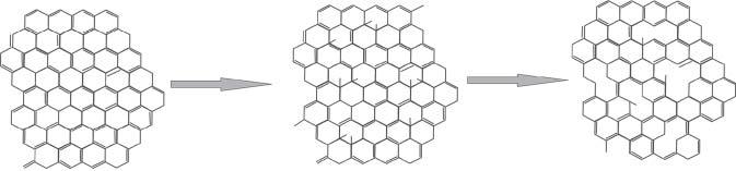
Graphiteoxideisacompoundofcarbon(C),oxygen(O),andhydrogen(H),andhas beensynthesizedbyHummers’methodin1958[2],usingthechemicalreactionbetween graphite,potassiumpermanganate(KMnO4 ),sodiumnitrate(Na2 NO3 ),andsulfuric acid(H2 SO4 ).Theone-molecule-thickorfew-layerversionofthesubstancegraphite oxideisknownasgrapheneoxide(GO).TheGOisnotconductivebutcanbereduced bychemicalreactions,thermaltreatment,ormanyothermethods,formingconductiverGO(Figure1.1)[3].Sofar,manymethodshavebeenwelldevelopedtosynthesis GOandrGO,includingthechemicalreduction,themicrowavemethod,theplasma method,thelasermethod,andthehydrothermalmethod.Othersynthesismethods, suchaschemicalvapourdeposition(CVD)method,arcdischargemethod,ballmilling approach,solvent-assistedexfoliation,etc.,werealsodevotedtodevelophigh-quality graphene,althoughthesesynthesismethodsallhavesometrade-offsintermsofhigh quality,highyield,andenvironmentalfriendliness.
Oxide (GO)Reduced Graphene Oxide (rGO)
Figure1.1 Thechemicalstructuresofgraphene,grapheneoxide(GO),thereducedgrapheneoxide (rGO)andtheconversionofgrapheneintoGOandrGOviaoxidation/reductionreactions.Source: Reprintedwithpermissionfromref. [3]Copyright2018,SpringerNature.
1.2SynthesisandCharacterizationsofGrapheneOxide
1.2.1ChemicalReductionofGrapheneOxide(GO)
Chemicalreductionofgrapheneoxide(GO)isacommonmethodtolow-costsynthesizegraphene[4].ExfoliationofGOtoindividualGOsheets(Figure1.2)couldbe chemicallyreducedtorGO,using,forinstance,NaBH4 orhydrazine[5].However,the producthasproblems,suchasaggregationanddefects.Moreover,thegenerallyused reducingagents,suchashydrazineorNaBH4 ,aretoxic.However,itstillremaineda greatchallengetoreadilyandefficientlysynthesisofhigh-qualitygraphenewithhigher conductivityandlessdefects.Recently,someemergingmethodsofproducinggraphene, suchasmicrowavemethod,plasmamethod,andlasermethod,haveattractedalotof interest,whichwillbepresentedinthefollowingsections.
1.2.2MicrowaveMethod
Microwaveabsorbsheatenergythroughthemediumandconductsmicro-gradient heatingfrominsidethematerial,whichisconsideredasauniquemethodformaterial
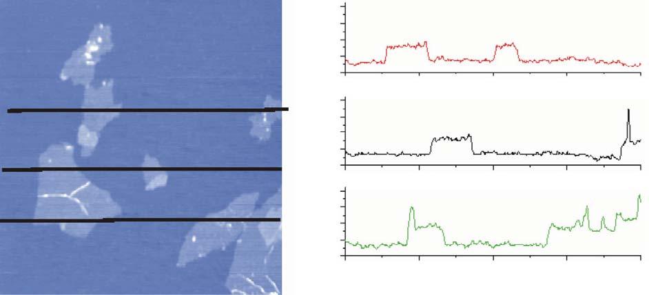
Figure1.2 AFMimageofexfoliatedgrapheneoxide(GO)sheetswiththreeheightprofilesacquiredin differentlocations.Source:Reprintedwithpermissionfromref.[5]Copyright2007ElsevierLtd.
3 synthesis.Thestrongmicrowaveabsorptioncapabilityofgrapheneoxide(GO)can quicklyremoveoxygen-containingfunctionalgroupsandfurtherexfoliatesGO.This featurehasafataltemptationforthepreparationofhigh-qualityandpollution-free graphene.Asearlyasin2011,microwavemethodwasemployedbyZhuetal.to exfoliateGO[6].ThroughthesubsequentactivationofKOH,theypreparedgraphene withahighspecificsurfacearea(SSA)valueof3100m2 g 1 andahighconductivityof 500Sm 1 .Anotherexampleofutilizationofmicrowavesistheexfoliationofgraphite inmolecularlyengineeredionicliquids[7].Itissupposedthatthecation–�� interactions canimprovetheaffinityofgraphenesurfaces.Theas-exfoliatedgrapheneexhibiteda highsingle-layerproportion.Besides, I D /I G valueof0.14andC/Oratioof30areclose tothevaluesofthegraphiteprecursor,indicatingtheexcellentstructuralintegrity. OneofthechallengesonproducingGOandrGOistheuseofthetoxicchemicals, suchassulfuricacidandhydrazinehydrate.Lotsofmethodshavebeendeveloped tosynthesizerGObygreenreductionmethods,usinghydroiodicacid(HI),citric acid,plantextracts,phytochemicals,oralternativelybythermalheatingintheinert atmosphere.In2016,Voiryetal.reportedonthefabricationofhigh-qualitygraphene throughthemicrowavereductionofGO[8].Thisresultattractedmuchinterestbecause theyusedaconventionalmicrowaveovenoperatedat1000Wtorapidlyandefficiently reduceGOnanosheetswith ∼50 μmsize(Figure1.3a).Thehigher-powermicrowave pulseslocallyandultra-fast-heatedGOuptoseveralthousanddegreestothoroughly eliminatetheoxygenfunctionalgroupsandreorderthegraphenebasalplane.The XPSresults(Figure1.3b)suggestthatmicrowave-reducedGO(MW-rGO)showsa negligiblein-planeoxygenconcentrationsof ∼4at.%.Thisoxygencontentismuch lowerthanthetheoreticalvalueofrGOannealedat1500K[9].TheRamanspectra ofMW-rGOandothercomparedsamplesareshowninFigure1.3c.Theas-prepared MW-rGOexhibitedhighlyorderedgraphene–likeRamanfeatureswithsharpand symmetrical2DandGpeaksandaverylow I D /I G ratio(<0.1).Itisalsofoundthat MW-rGOshowshigher I 2D /I G ratiosandlargergraphenedomainsizesascompared withrGOandsolution-exfoliatedflakes(Figure1.3d).Althoughmicrowavemethod haspotentialadvantagesintheefficientpreparationofhigh-qualitygraphene,itshould benotedthattheyieldissolowthatscale-upfabricationofhigh-qualitygraphene remainsagreatchallenge.
1.2.3PlasmaMethod
Plasmaetchingmaynotbeabletopreciselycontrolthemicrostructureoftheproduct attheatomiclevel,andevenmayentailundefinedstructuraldisordersordefectsofthe products.However,asasimpleandefficientmethod,plasmaetchingstillwaswidely usedforetchingofcarbonmaterials[10].Graphenewasoncepreparedbyunzipping ofcarbonnanotubes(CNTs)throughplasmaetchingwithpoly(methylmethacrylate) (PMMA)films[10].Herein,PMMAprotectsCNTsasanetchingmaskduringtheetchingprocess.ThetopsidewallsofCNTswereetchedfasterandremovedbytheplasma. For10secondsofAgron(Ar)plasmaetching,20%ofthestartingCNTswereconverted intosingle-orfew-layergraphenenanoribbons(GNRs)with ∼10–20nmwidthand 2nmheight.Pangetal.reportedonthepatternedGNsynthesizedbymeansofan oxygen-plasmaetchingapproachfromsolution-processedGOfilms[11].Theyused low-costaluminiumassacrificialmetalandprotectivemaskstoremovethegraphene
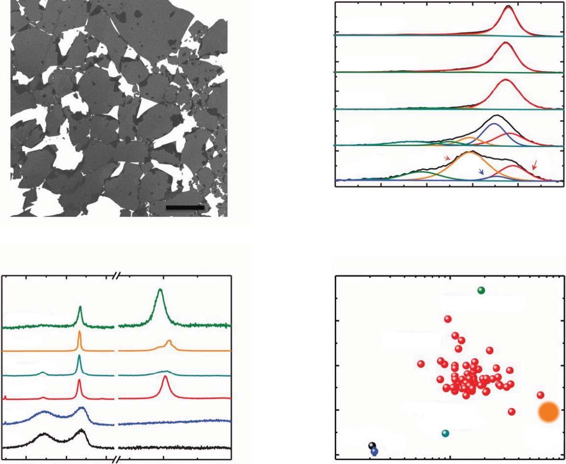
Figure1.3 (a)SEMofGOnanosheets.(b)High-resolutionXPSC1sspectraand(c)Ramanspectraof MW-rGOandothercomparedsamples.(d)Evolutionofthe I2D /IG ratioversusthecrystalsize(La).
Source:Reprintedwithpermissionfromref.[8]Copyright2016TheAmericanAssociationforthe AdvancementofScience(AAAS).
regionsnotcoveredbythealuminiumwhenthesamplewasexposedtooxygenplasma. Theyarguedthatoxygen-plasmaetchingofgraphenefilmwithsacrificialaluminium contactpatternsisaneffectivemethodforaccuratelycontrollingthesizeofgraphene electrodes.WangandcoworkersreportedthepreparationofgraphenefromtheGO usingaradiofrequency(RF)dielectricbarrierdischargeplasmasystemwithdifferent plasmagas,suchasO2 ,N2 ,andCH4 [12].
1.2.4LaserMethod
Thelasermethodforthefabricationofgraphenehasadvantagesovertheconventional methodsrequiringhighsynthesistemperatureortediouspost-treatments.Lasertechnologiesenabledtheprocesstobesimplerandmorecompatible.Althoughthistechnologystillfacestheproblemoflarge-scaleproduction,ithasbeendemonstratedto producehigh-qualitygraphene.El-Kadyetal.usedastandardLightScribeDVDopticaldrivetocarryoutthedirectlaserreductionofGOfilmstoGNwithhighelectrical conductivity(1738Sm 1 )andSSA(1520m2 g 1 ),whichcanbeuseddirectlyassupercapacitorelectrodeswithoutthebinderorcurrentcollectors[13].TheLightScribelaser

Figure1.4 (a)PreparationillustrationofLSGandSEMimagesofcross-sectionoftheproduct.Source: Reprintedwithpermissionfromref.[13]Copyright2012TheAmericanAssociationforthe AdvancementofScience(AAAS).Morphologycharacterizationsoflaser-inducedgraphene(LIG) derivedfrompine:(b)SEMimageofpristinepine,(c)SEM,(d)TEMand(e)high-resolutionTEMimages ofP-LIG-70.Thescalebarsare500 μm,500 μm,20nm,and4nm,respectively.Source:Reprintedwith permissionfromref.[14]Copyright2017TheWiley-VCH.(f)Schematicillustratingthepreparation processofsolid-stateflexibleMG-MSCs.Source:Reprintedwithpermissionfromref.[15]Copyright 2018Wiley-VCH.
wasabletosimultaneouslyreduceandexfoliatetheGOsheetstoformanopennetwork oflaser-scribedgraphene(LSG)(Figure1.4a).Thisnetworkstructurewithopenpores integratesthepositiveintermsofpreventingtheagglomerationofgraphenesheetsand facilitatingtheelectrolyteaccessibilitytoimprovetheionicdiffusion.
1.3EnergyHarvestApplicationsofGrapheneOxide
1.3.1SolarCells
Thesuperiorelectronicandopticalpropertiesofgraphenemadeitanidealcandidate forvariousenergyharvestdeviceapplications.GrapheneandrGOcouldbeusedasthe
Figure1.5 Illustrationandperformanceofsolarcellbasedongrapheneelectrodes.(a)Illustrationof dye-sensitizedsolarcellusinggraphenefilmaselectrode,thefourlayersfrombottomtotopareAu, dye-sensitizedheterojunction,compactTiO2 ,andgraphenefilm.(b)Theenergyleveldiagramof graphene/TiO2 /dye/spiro-OMeTAD/Audevice.(c)I-Vcurveofgraphene-basedcell(black)andthe FTO-basedcell(grey),illuminatedunderAMsolarlight(1sun).Source:Reprintedwithpermissionfrom ref.[16]Copyright2008TheAmericanChemicalSociety.
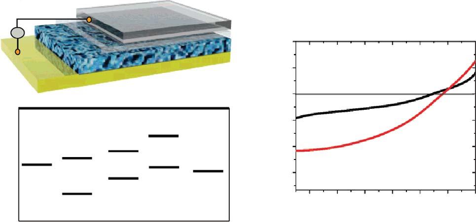
transparentelectrode,counterelectrode,orinterfacelayersinsolarcelldevices.Wang, Zhi,andMüllenreportedtheultra-thintransparentconductiveelectrodeofrGOfilms forthesolid-statedye-sensitizedsolarcells(DSSC;Figure1.5a).TheGOproducedby theHummersmethodwerepurifiedanddispersedinDIwater,the5–20-nm-thickGO filmsweredepositedonthesubstratebydipcoatingfollowedbythethermalreduction. ThesheetresistanceoftherGOwasabout1.8kΩ/sq,calculatedconductivitywasabout 550Scm 1 andatransparencyofmorethan70%over1000–3000nm.TheworkfunctionofrGOis4.42eV(Figure1.5b),closetothethatofFTOelectrode(4.4eV).When servedastheanode,thegraphene/TiO2 /dye/spiro-OMeTAD/AuDSSCdevicedemonstratedashort-circuitphotocurrentdensity(I sc )of1.01mAcm 2 withanopen-circuit voltage(V oc )of0.7V.Thecalculatedfillingfactor(FF)was0.36andthepowerconversionefficiencywas0.26%(Figure1.5c)[16].
Edaetal.reportedtheuseofrGOthinfilmspreparedbyvacuumfiltrationandtransferfortheorganicsolarcells[17].TheGOdispersionwasfilteredthrougha25-nm pore-sizemixedcelluloseestermembrane,thentheobtainedfilmsweretransferred ontothesubstrateandtheestermembranewasthenremovedbyacetonewashes.The GOwasreducedbythehydrazinevapourandlowtemperatureannealingat200 ∘ C.The sheetresistanceoftherGOfilmwasveryhigh,about70kΩ/sqwhenthetransmittance ofthefilmisapproximately65%.Theysuccessfullyreducedthesheetresistancenearly byafactorof5whenbydippinginthionylchloride(SOCl2 )for1hour.TheOPVdevices withtherGOfilmswereverylow,onlyabout0.1%duetotheverylargesheetresistance (ontheorderof105 ).
Wuetal.usedtheGOasthedualfunctionalinterfacemodifierforimprovingwettabilityandretardingrecombinationinindiumtinoxide(ITO)/GO/CH3 NH3 PbI3-x Clx / PCBM/ZnO/Alhybridperovskitesolarcells[18].TheGOservicedasthebuffer
1.4EnergyStorageApplicationsofGrapheneOxide 7
layerbetweentheperovskiteand2,2′ ,7,7′ -tetrakis-(N,N-di-p-methoxyphenyl-amine)9,9′ -spirobifluorene(Spiro-MeOTAD)holetransportlayer(HTL).Theopen-circuit voltage(V OC )andthefillfactor(FF)improvedandtheaverageefficiencygreatly increasedby45.5%,from10.0%to14.5%.Wangetal.fabricatedhighefficiency(up to15.6%)solarcellswithperovskitematerialsandthenanocompositesofsolvent exfoliatedgrapheneandTiO2 usinglowtemperaturesolutionprocesses(nohigher than150 ∘ C).Thegraphenenanoflakesprovidesuperiorcharge-collectioninthe nanocomposites[19].
1.3.2SolarThermalEnergyHarvestDevices
ThebroadbandopticalabsorptionpropertiesandthehighsurfaceofrGOmade itanidealcandidateforthesolarthermalenergyharvestandsolarthermalenergy ultilizations.Itoetal.reportedtheuseofgraphenegrownbyCVDforthesolarabsorber andtheheatlocalizationmaterialforsteamgeneration[20],high-energyconversion efficiencyof80%andfastwaterevaporationrateof1.50kgm 2 h 1 wereachieved.Hu etal.preparerGO-CNTaerogelsanddemonstratehighefficiency(83%)solarsteam generationunderonesun[20].Liuetal.designandpreparedthecarbon–carbon compositematerialsbasedonrGOandcarbonclothbyelectrochemistryreduction ofGO(Figure1.6a)[21].TherGO-carbonclothhasultra-highsolarabsorptionup to93–97%,thusaultra-highevaporationrate2.54kgm 2 h 1 wasachievedunder normalilluminationof1kWm 2 .Theconductingnatureofthesolaropticalabsorber layerallowstheuseoflow-voltageelectricityasanadditionalenergyinput.The flexiblecarboncompositingfilmcouldreach389 ∘ Cwithin10secondsatonly3.5V (Figure1.6b,c).TheelectricallypoweredJouleheatingboostedthesteamgeneration ratebyorderofmagnitude,settingtherecordhighvalueoftheinterfacialevaporation andsteamgenerationupto45.87kgm 2 h 1 .
GrapheneoxideandrGOhavealsobeenusedinotherenergyharvestdevices,such asthermalenergyharvesting[22],themechanicalenergyharvesting[23],theacoustic energy[24]harvesting,andsoon.Besidesusinggrapheneonitsown,itcanalsobe compositedorhybridwithothermaterialstoenhancetheperformanceoftheenergy harvestdevices.
1.4EnergyStorageApplicationsofGrapheneOxide
1.4.1Supercapacitors
Sinceitsfirstapplicationinsupercapacitorsin2008[25],graphenewithitshightheoreticalSSA(2630m2 g 1 ),excellentelectronicconductivity,highflexibility,andsurfacefunctionalizeddiversity,isregardedasapotentialcandidateforbothelectrical double-layercapacitance(EDLC)andpseudocapacitance-basedsupercapacitors.Ruoff etal.preparedtheactivatedgraphenebysimpleactivationwithKOHofmicrowave exfoliatedGO(MEGO)[6].TheMEGOhasultra-highsurfaceareaupto3100m2 g 1 , containingmicroporesandmesoporeswithsizesdistributedbetween ∼1nmand10nm. SupercapacitorsbasedontheMEGOshowedahighgravimetriccapacitanceof166Fg 1 andanexcellentenergydensityof ∼70Whkg 1 . Althoughgrapheneshowedexcellentpowerdensityandcyclicstability,theirspecific capacitancesstillhavealargegapcomparedtothetheoreticalvalueof550Fg 1 [20].

Figure1.6 ThepreparationofGO-CCandrGO-CCcomposites.(a)Theelectrochemicaldepositionof graphene.(b)Theschematicdiagramofelectrochemicaldepositionandjouleheatingprocessto obtainrGOoncarbonclothsamples.(c)TheschematicdiagramofrGO-CCcompositeheating elementstogeneratewatervapourwithlowvoltage.(d–g)Thephotographsandinfraredphotosof therGO-CC(flatandbending).Source:Reprintedwithpermissionfromref.[21]Copyright20202020 WILEY-VCHVerlagGmbH&Co.KGaA,Weinheim.
Thisiscausedbyintrinsicaggregationorre-stackingofgraphenenanosheets(GNSs) duetothestrongvanderWaalsforces,resultinginaseriouslyreducedelectrochemical property.Nevertheless,thishasnotaffectedpeople’senthusiasmfortheapplication ofgrapheneinsupercapacitorsoverthepastdecade.Inthissection,wewillfocus onthefollowingaspects:theemergingpreparationmethodsforgraphene,howto tunetheinterlayerspacingofgraphenetoachievebetterelectrochemicalproperties, three-dimensional(3D)porousgraphene,andgrapheneaerogels.
Itisgenerallyconsideredthatinvestigationofhowiontransportthroughcomplexlayeredgraphene-basedmembranesisdifficultbecauseoftherandomdistributionofmultiscalecomplexandimperfectnanoslitsornanochannelswithinthelayeredgraphenes. Usingalayeredgraphenegel(LGG)asatargetplatformpreparedfollowingthepreviouslyreported‘capillarycompression’method,Chengetal.demonstratedtheeffects oftuneableinterlayerspacingonthetransportpropertiesofionswithexperimentand simulation[26].Theexperimentallyestimatedinterlayerspacing(d exp )canbevaried intheregionofbelow10nm(Figure1.7aTop).Additionally,smallangleneutronscattering(SANS)measurementwascarriedouttoprobetherestackphenomenoninthe as-compressedLGGmembranes(Figure1.7a,bottom).

Figure1.7 (a)Top:SEMimagesoftheLGGmembraneswhencompressedto3.2nm(left)and0.5nm (right),respectively.Bottom:Smallangleneutronscattering(SANS)patternsofthemembraneswith d exp of3.9nm(left)and0.5nm(right),respectively.(b)Aschematicillustrationoftheformationof nanoslitsarray.(c)Reduced1DSANSdataoffsetfromtheabsoluteintensityscale.Theupperright insetistheslope F asafunctionof d exp .Source:Reprintedwithpermissionfromref.[26]Copyright 2016,TheAmericanAssociationfortheAdvancementofScience(AAAS).(d)Schematicdiagram illustratingtheproductionofEGM-GOfilms.(e)SchematicillustrationoftheASSCconfigurationand digitalphotosofthesolid-stateelectrolyte,theflexibleASSC,andtheASSCundervariousbending angles.(f)Cross-sectionalSEMimagesofrGOfilmand(g)EGM-rGO(50%EG)film.Scalebars,2 μm. Source:Reprintedwithpermissionfromref.[27]Copyright2020,NaturePublishingGroup.
Inordertoestablishaquantitativerelationshipamongthenanoconfinediontransport propertiesinrelationtothecomplexnanoporousstructureofthelayeredmembrane, theyconstructedarepresentativestructuralmodeltodescribethefluidiccontourscontainedintheLGGmembranes(Figure1.7b),inwhichtheheightofnanoslits(d ),thelateralsizeofindividualnanosheets(L),andthegapdistancebetweentheendsofthesheets (�� )arethekeygeometricalvariablesoftheproposedstructuralmodel.Thereduced1D SANScurvesinFigure1.7cfurtherconfirmedthatthenanospaceandtheporousstructureintheLGGmembranesremainslargelycontinuous.Theseresultsrevealednew insightsintotheiontransportphenomenaconfinedinagraphenenanochanneland providedasolidfoundationfortheapplicationofGNSsinsupercapacitors.
Recently,Lietal.preparedafreestandinggraphenelaminatefilmelectrodewithhighly efficientporeutilizationforcompactcapacitiveenergystorage[27].Theenhancement ofporeutilizationwasachievedbypreciselyadjustingtheinterlayerspacingofthisfilm