Organic Semiconductors for Optoelectronics 1st Edition Hiroyoshi Naito
Visit to download the full and correct content document: https://ebookmass.com/product/organic-semiconductors-for-optoelectronics-1st-editio n-hiroyoshi-naito/
More products digital (pdf, epub, mobi) instant download maybe you interests ...
Understanding Semiconductors 1st Edition Corey Richard
https://ebookmass.com/product/understanding-semiconductors-1stedition-corey-richard/
Nanoparticle Technology Handbook 3rd Edition Makio Naito
https://ebookmass.com/product/nanoparticle-technologyhandbook-3rd-edition-makio-naito/
Metal Oxides for Optoelectronics and Optics-Based Medical Applications Suresh Sagadevan
https://ebookmass.com/product/metal-oxides-for-optoelectronicsand-optics-based-medical-applications-suresh-sagadevan/
Understanding Semiconductors: A Technical Guide for Non-Technical People (Maker Innovations Series) 1st Edition Corey Richard
https://ebookmass.com/product/understanding-semiconductors-atechnical-guide-for-non-technical-people-maker-innovationsseries-1st-edition-corey-richard/
Metal-Organic Frameworks for Chemical Reactions: From Organic Transformations to Energy Applications 1st Edition Anish Khan (Editor)
https://ebookmass.com/product/metal-organic-frameworks-forchemical-reactions-from-organic-transformations-to-energyapplications-1st-edition-anish-khan-editor/
Organic Electronics for Electrochromic Materials and Devices 1st Edition Hong Meng
https://ebookmass.com/product/organic-electronics-forelectrochromic-materials-and-devices-1st-edition-hong-meng/
Organic Synthesis Using Biocatalysis 1st Edition
Goswami
https://ebookmass.com/product/organic-synthesis-usingbiocatalysis-1st-edition-goswami/
Metal-free synthetic organic dyes Kruger
https://ebookmass.com/product/metal-free-synthetic-organic-dyeskruger/
eBook Online Access for Organic Chemistry 10th Edition, (Ebook PDF)
https://ebookmass.com/product/ebook-online-access-for-organicchemistry-10th-edition-ebook-pdf/
OrganicSemiconductorsforOptoelectronics
WileySeriesinMaterialsforElectronicand OptoelectronicApplications
www.wiley.com/go/meoa
SeriesEditors
RichardCurry,UniversityofManchester,Manchester,UK
HarryRuda,UniversityofToronto,Toronto,Canada
JunLuo,ChineseAcademyofSciences,Beijing,China
HonorarySeriesEditors
ProfessorArthurWilloughby, UniversityofSouthampton,Southampton,UK
DrPeterCapper, Ex-LeonardoMWLtd,Southampton,UK
ProfessorSafaKasap, UniversityofSaskatchewan,Saskatoon,Canada
PublishedTitles
BulkCrystalGrowthofElectronic,OpticalandOptoelectronicMaterials,EditedbyP.Capper PropertiesofGroup-IV,III—VandII—VISemiconductors,S.Adachi ChargeTransportinDisorderedSolidswithApplicationsinElectronics,EditedbyS.Baranovski OpticalPropertiesofCondensedMatterandApplications,EditedbyJ.Singh ThinFilmSolarCells:Fabrication,Characterization,andApplications,EditedbyJ.PoortmansandV. Arkhipov
DielectricFilmsforAdvancedMicroelectronics,EditedbyM.R.Baklanov,M.Green,andK.Maex LiquidPhaseEpitaxyofElectronic,OpticalandOptoelectronicMaterials,EditedbyP.CapperandM. MaukMolecularElectronics:FromPrinciplestoPractice,M.Petty LuminescentMaterialsandApplications,A.Kitai CVDDiamondforElectronicDevicesandSensors,EditedbyR.S.Sussmann PropertiesofSemiconductorAlloys:Group-IV,III—VandII—VISemiconductors,S.AdachiMercury CadmiumTelluride,EditedbyP.CapperandJ.Garland ZincOxideMaterialsforElectronicandOptoelectronicDeviceApplications,EditedbyC.Litton,D. C.Reynolds,andT.C.Collins
Lead-FreeSolders:MaterialsReliabilityforElectronics,EditedbyK.N.SubramunianSilicon Photonics:FundamentalsandDevices,M.JamalDeenandP.K.Basu NanostructuredandSubwavelengthWaveguides:FundamentalsandApplications,M.Skorobogatiy PhotovoltaicMaterials:FromCrystallineSilicontoThird-GenerationApproaches,EditedbyG. ConibeerandA.Willoughby GlancingAngleDepositionofThinFilms:EngineeringtheNanoscale,MatthewM.Hawkeye,Michael T.Taschuk,andMichaelJ.Brett PhysicalPropertiesofHigh-TemperatureSuperconductors,R.Wesche SpintronicsforNextGenerationInnovativeDevices,EditedbyKatsuakiSatoandEijiSaitohInorganic GlassesforPhotonics:Fundamentals,EngineeringandApplications,AnimeshJha AmorphousSemiconductors:Structural,OpticalandElectronicProperties,KazuoMorigaki,Sandor Kugler,andKoichiShimakawa MicrowaveMaterialsandApplications,Twovolumeset,EditedbyMailadilT.Sebastian,RickUbic, andHeliJantunen MolecularBeamEpitaxy:MaterialsandApplicationsforElectronicsandOptoelectronics,Editedby HajimeAsahiandYoshijiKorikoshi MetalorganicVaporPhaseEpitaxy(MOVPE):Growth,MaterialsProperties,andApplications,Edited byStuartIrvineandPeterCapper OpticalPropertiesofMaterialsandTheirApplications,SecondEdition,EditedbyJaiSingh OxideElectronics,EditedbyAsimRay
OrganicSemiconductorsforOptoelectronics
Editedby HiroyoshiNaito
OsakaPrefectureUniversity Osaka,Japan
Thiseditionfirstpublished2021
©2021JohnWileyandSonsLtd
Allrightsreserved.Nopartofthispublicationmaybereproduced,storedinaretrievalsystem,or transmitted,inanyformorbyanymeans,electronic,mechanical,photocopying,recordingorotherwise, exceptaspermittedbylaw.Adviceonhowtoobtainpermissiontoreusematerialfromthistitleisavailable athttp://www.wiley.com/go/permissions.
TherightofHiroyoshiNaitotobeidentifiedastheauthoroftheeditorialmaterialinthisworkhasbeen assertedinaccordancewithlaw.
RegisteredOffices
JohnWiley&Sons,Inc.,111RiverStreet,Hoboken,NJ07030,USA
JohnWiley&SonsLtd,TheAtrium,SouthernGate,Chichester,WestSussex,PO198SQ,UK
EditorialOffice
TheAtrium,SouthernGate,Chichester,WestSussex,PO198SQ,UK
Fordetailsofourglobaleditorialoffices,customerservices,andmoreinformationaboutWileyproducts visitusatwww.wiley.com.
Wileyalsopublishesitsbooksinavarietyofelectronicformatsandbyprint-on-demand.Somecontentthat appearsinstandardprintversionsofthisbookmaynotbeavailableinotherformats.
LimitofLiability/DisclaimerofWarranty
Inviewofongoingresearch,equipmentmodifications,changesingovernmentalregulations,andthe constantflowofinformationrelatingtotheuseofexperimentalreagents,equipment,anddevices,thereader isurgedtoreviewandevaluatetheinformationprovidedinthepackageinsertorinstructionsforeach chemical,pieceofequipment,reagent,ordevicefor,amongotherthings,anychangesintheinstructionsor indicationofusageandforaddedwarningsandprecautions.Whilethepublisherandauthorshaveused theirbesteffortsinpreparingthiswork,theymakenorepresentationsorwarrantieswithrespecttothe accuracyorcompletenessofthecontentsofthisworkandspecificallydisclaimallwarranties,including withoutlimitationanyimpliedwarrantiesofmerchantabilityorfitnessforaparticularpurpose.Nowarranty maybecreatedorextendedbysalesrepresentatives,writtensalesmaterialsorpromotionalstatementsfor thiswork.Thefactthatanorganization,website,orproductisreferredtointhisworkasacitationand/or potentialsourceoffurtherinformationdoesnotmeanthatthepublisherandauthorsendorsethe informationorservicestheorganization,website,orproductmayprovideorrecommendationsitmaymake. Thisworkissoldwiththeunderstandingthatthepublisherisnotengagedinrenderingprofessionalservices. Theadviceandstrategiescontainedhereinmaynotbesuitableforyoursituation.Youshouldconsultwitha specialistwhereappropriate.Further,readersshouldbeawarethatwebsiteslistedinthisworkmayhave changedordisappearedbetweenwhenthisworkwaswrittenandwhenitisread.Neitherthepublishernor authorsshallbeliableforanylossofprofitoranyothercommercialdamages,includingbutnotlimitedto special,incidental,consequential,orotherdamages.
LibraryofCongressCataloging-in-PublicationData
Name:Naito,Hiroyoshi,editor.
Title:Organicsemiconductorsforoptoelectronics/editedbyHiroyoshi Naito.
Description:Firstedition.|Hoboken,NJ:Wiley,2021.|Series:Wiley seriesinmaterialsforelectronicandoptoelectronicapplications| Includesbibliographicalreferencesandindex.
Identifiers:LCCN2020051135(print)|LCCN2020051136(ebook)|ISBN 9781119146100(hardback)|ISBN9781119146117(adobepdf)|ISBN 9781119146124(epub)
Subjects:LCSH:Organicsemiconductors.|Optoelectronics.
Classification:LCCQC611.8.O7O69672021(print)|LCCQC611.8.O7 (ebook)|DDC537.6/223–dc23
LCrecordavailableathttps://lccn.loc.gov/2020051135
LCebookrecordavailableathttps://lccn.loc.gov/2020051136
CoverDesign:Wiley
CoverImages:CourtesyandCopyrightofNIPPONSHOKUBAICO.,LTD Setin10/12ptWarnockProbyStraive,Chennai,India
10987654321
Contents
ListofContributors xiii
SeriesPreface xv
Preface xvii
1ElectronicStructuresofOrganicSemiconductors1
KazuyoshiTanaka
1.1Introduction1
1.2ElectronicStructuresofOrganicCrystallineMaterials2
1.2.1Free-ElectronPicture3
1.2.2Tight-BindingFramework4
1.2.2.1Formalism4
1.2.2.2SimpleExample7
1.2.3ElectronicPropertiesBasedontheElectronicStructure9
1.2.3.1CharacteristicsoftheEnergyBand9
1.2.3.2BandGap(ΔE g )11
1.2.3.3FermiEnergy(��F )andFermiLevel(E F )11
1.2.3.4BandWidth(W)12
1.2.3.5IonizationPotential(I p )12
1.2.3.6ElectronAffinity(E a )13
1.2.3.7DensityofStates(DOS)13
1.2.3.8EffectiveMass(m*)14
1.2.3.9COPattern14
1.2.3.10ElectronDensityandBondOrder14
1.2.3.11TotalEnergyof1DCrystal(E tot )15
1.2.3.12Mobility15
1.3InjectionofChargeCarriers16
1.3.1OrganicConductivePolymers17
1.3.2OrganicCharge-TransferCrystals19
1.4TransitionfromtheConductiveState26
1.4.1PeierlsTransition26
1.4.1.1Polyacetylene27
1.4.1.2TTF-TCNQ28
1.4.2CompetitionofSpinDensityWaveandSuperconductivity29
1.5ElectronicStructureofOrganicAmorphousSolid30
1.5.1ExaminationofElectronicStructures31
1.5.1.1DirectCalculationoftheLocalStructure32
1.5.1.2Effective-MediumApproximation33
1.5.2LocalizedLevelsandMobilityEdge33
1.5.3HoppingProcess33
1.5.3.1HoppingProcessbetweentheNearestNeighbors34
1.5.3.2VariableRangeHopping(VRH)36
1.5.3.3HoppingProcessviatheDopants37 1.6Conclusion37 Acknowledgment38 References38
2ElectronicTransportinOrganicSemiconductors41
HiroyoshiNaito
2.1Introduction41
2.2AmorphousOrganicSemiconductors41
2.2.1MeasurementsofTransportProperties43
2.2.1.1Time-of-FlightTransientPhotocurrent Experiment43
2.3ExperimentalFeaturesofElectronicTransportProperties44
2.4ChargeCarrierTransportModels44
2.4.1MultipleTrappingModel45
2.4.2GaussianDisorderModel(GDM)48
2.4.3CorrelatedDisorderModel(CDM)49
2.4.4GDMvs.CDM49
2.4.5PolaronicTransport50
2.4.6TransportEnergy50
2.4.7AnalyticalApproachtoHoppingTransport51
2.4.8FunctionalFormsofLocalizedStateDistributions52
2.5PredictionofTransportPropertiesinAmorphousOrganic Semiconductors52
2.6PolycrystallineOrganicSemiconductors53
2.6.1TransportinPolycrystallineSemiconductorsand TechnologicalImportanceofPolycrystallineSilicon53
2.6.2Field-EffectMobilityinOrganicPolycrystalline Semiconductors55
2.6.3PerformanceofField-EffectTransistorswithPolycrystalline OrganicSemiconductors58
2.7Single-CrystallineOrganicSemiconductors59
2.7.1BandConductioninSingle-CrystallineOrganic Semiconductors61
2.7.2PerformanceofField-EffectTransistorswithSingle CrystallineOrganicSemiconductors64
2.8ConcludingRemarks65 Acknowledgment65 References65
3TheoryofOpticalPropertiesofOrganicSemiconductors69
JaiSingh,MonishkaRitaNarayanandDavidOmpong
3.1Introduction69
3.2PhotoexcitationandFormationofExcitons70
3.2.1PhotoexcitationofSingletExcitonsduetoExciton-photon Interaction71
3.2.2ExcitationofTripletExcitons74
3.2.2.1DirectExcitationtoTripletStatesThrough Exciton-Spin-Orbit-PhotonInteraction74
3.2.2.2IndirectExcitationofTripletExcitonsThrough IntersystemCrossingandExciton-SpinOrbit-PhononInteraction79
3.3ExcitonupConversion83
3.4ExcitonDissociation85
3.4.1ProcessofConversionfromFrenkeltoCTExcitons88
3.4.2DissociationofCTExcitons89 References90
4LightAbsorptionandEmissionPropertiesofOrganicSemiconductors93
TakashiKobayashi,TakashiNagaseandHiroyoshiNaito
4.1Introduction93
4.2ElectronicStatesinOrganicSemiconductors94
4.2.1FluorescenceEmitters95
4.2.2PhosphorescenceEmitters97
4.2.3TADFEmitters99
4.2.4 π ConjugatedPolymers100
4.3DeterminationofExcited-stateStructureUsingNonlinear Spectroscopy102
4.3.1Background103
4.3.2ExperimentalTechnique106
4.3.2.1EA106
4.3.2.2TPE107
4.3.3ExperimentalResults109
4.3.3.1DE2109
4.3.3.2Ir(ppy)3 111
4.3.3.3PFO113
4.4DecayMechanismofExcitedStates115
4.4.1Background115
4.4.2ExperimentalTechnique117
4.4.2.1Time-resolvedPLMeasurements117
4.4.2.2PLQEMeasurements120
4.4.3ExperimentalResults121
4.4.3.1PFO121
4.4.3.2Ir(ppy)3 123
4.4.3.34CzIPN127
4.5Summary132 Acknowledgement132 References132
5CharacterizationofTransportPropertiesofOrganicSemiconductorsUsing ImpedanceSpectroscopy137
KenichiroTakagiandHiroyoshiNaito
5.1Introduction137
5.2Charge-CarrierMobility138
5.2.1MethodsforMobilityMeasurements138
5.2.2TheoreticalBasisforDeterminationofCharge-Carrier Mobility139
5.2.3DeterminationofCharge-CarrierMobility141
5.2.4InfluenceofBarrierHeightforCarrierInjectionon DeterminationofCharge-CarrierMobility142
5.2.5InfluenceofContactResistanceonDeterminationof Charge-CarrierMobility143
5.2.6InfluenceofLocalizedStatesonDeterminationof Charge-CarrierMobility144
5.2.7DemonstrationofDeterminationofCharge-Carrier Mobility146
5.3Localized-StateDistributions148
5.3.1MethodsforLocalized-StateMeasurements148
5.3.2TheoreticalBasisforDeterminationofLocalized-State Distribution149
5.3.3DemonstrationofDeterminationofLocalized-State Distribution150
5.4Lifetime153
5.4.1MethodsforDeep-Trapping-LifetimeMeasurements153
5.4.2DeterminationofDeep-Trapping-Lifetimeusingthe ProposedMethod153
5.4.3ValidityoftheProposedMethod154
5.4.4DemonstrationofDeterminationofDeepTrapping-Lifetime155
5.5ISinOLEDsandOPVs156
5.6Conclusions156 Acknowledgments157 References157
6Time-of-FlightMethodforDeterminingtheDriftMobilityinOrganic Semiconductors161
MasahiroFunahashi
6.1Introduction161
6.2PrincipleoftheTOFMethod162
6.2.1CarrierMobilityandTransientPhotocurrent162
6.2.2StandardSetupoftheTOFMeasurement163
6.2.3SamplePreparation164
6.2.4CurrentModeandChargeMode165
6.2.5InstructionsintheTOFMeasurements167
6.3InformationObtainedFromtheTOFExperiments172
6.4TechniquesRelatedtotheTOFMeasurement173
6.4.1XerographicTOFMethod173
6.4.2LateralTOFMethod174
6.4.3TOFMeasurementsUnderPulseVoltageApplication175
6.4.4DarkInjectionSpaceCharge-LimitedTransientCurrent Method175 6.5Conclusion177 References177
7MicrowaveandTerahertzSpectroscopy179 AkinoriSaeki
7.1Introduction179
7.2InstrumentalSetupofTime-ResolvedGigahertzandTerahertz Spectroscopies181
7.3TheoryofComplexMicrowaveConductivityinaResonantCavity183
7.4MicrowaveSpectroscopyforOrganicSolarCells185
7.5Frequency-Modulation:InterplayofFreeandShallowly-Trapped Electrons187
7.6Organic-InorganicPerovskite195
7.7Conclusions197 Acknowledgement198 References198
8IntrinsicandExtrinsicTransportinCrystallineOrganicSemiconductors: Electron-Spin-ResonanceStudyforCharacterizationofLocalizedStates201 AndreyS.Mishchenko
8.1IntrinsicandExtrinsicTransportinCrystallineOrganic Semiconductors203
8.2ElectronSpinResonanceStudyforCharacterizationofLocalized States206
8.2.1IntroductionintoESRStudy206
8.2.2ESRSpectraofTrappedCarriers208
8.2.2.1ESRSpectraforSingleMoleculeandaCluster ContainingSeveralMolecules208
8.2.2.2ESRSpectraforaTrapinCrystal209
8.2.2.3ESRSpectraforSeveralKindsofTraps210
8.2.3FromESRSpectrumtoTrapDistributionOverDegreeof Localization211
8.2.3.1MethodtoSolveInverseProblem211
8.2.3.2TestsofSOMStabilityAgainsttheNoisein ExperimentalData212
8.2.3.3PracticalImplementationofMethod:Distribution ofTrapsinPentaceneTFT213
8.2.3.4ReliabilityofTrapDistributionResult214
8.2.4TransformationFromSpatialDistributiontoEnergy Distribution214
8.2.4.1TrapModel:2DHolsteinPolaronandOn-Site AttractiveCenter215
8.2.4.2EnergyDistributionofTrapsinPentaceneTFTs216
8.2.5Discussion217
8.2.6SummaryofTrapStudy218 8.3Conclusion219 Acknowledgments219 References220
9SecondHarmonicGenerationSpectroscopy225 TakaakiManakaandMitsumasaIwamoto
9.1Introduction225
9.2BasicsoftheEFISHG226
9.2.1MacroscopicOriginoftheSHG226
9.2.2MicroscopicDescriptionoftheSHG228
9.2.3EFISHGMeasurements229
9.2.4EvaluationofIn-planeElectricFieldinOFET231
9.2.5DirectImagingofCarrierMotioninOFET232
9.3SomeApplicationoftheTRM-SHGtotheOFET234
9.3.1TrapEffect234
9.3.2MetalElectrodeDependence237
9.3.3AnisotropicCarrierTransport239
9.4ApplicationoftheTRM-SHGtoOLED240
9.5Conclusions242 Acknowledgement243 References243
10DevicePhysicsofOrganicField-effectTransistors245 HiroyukiMatsui
10.1OrganicField-EffectTransistors(OFETs)245
10.1.1StructureofOFETs245
10.1.2OperationPrinciplesofOFETs248
10.1.3CarrierTraps251
10.1.4TransportModelsinChannels252
10.1.4.1BandTransportModel253
10.1.4.2MultipleTrapandReleaseModel256
10.1.4.3HoppingModel259
10.1.4.4DynamicDisorderModel260
10.1.4.5GrainBoundaryModel263
10.1.5CarrierInjectionatSourceandDrainElectrodes264
10.1.5.1TransmissionLineMethod(TLM)266
10.1.5.2Four-TerminalMeasurement267
10.1.5.3EffectofContactResistanceonApparentMobility268 References270
11SpontaneousOrientationPolarizationinOrganicLight-EmittingDiodes anditsInfluenceonChargeInjection,Accumulation,andDegradation Properties273
YutakaNoguchi,HisaoIshii,LarsJäger,TobiasD.SchmidtandWolfgangBrütting 11.1Introduction273
11.2InterfaceChargeModel275
11.3InterfaceChargeinBilayerDevices277 11.4ChargeInjectionProperty281 11.5DegradationProperty283 11.6Conclusions290 Acknowledgement291 References292
12AdvancedMolecularDesignforOrganicLightEmittingDiodeEmittersBased onHorizontalMolecularOrientationandThermallyActivatedDelayed Fluorescence295
LiZhao,DaeHyeonKim,Jean-CharlesRibierre,TakeshiKominoandChihayaAdachi 12.1Introduction295
12.2MolecularOrientationinTADFOLEDs299
12.3MolecularOrientationinSolutionProcessedOLEDs300 References304
13OrganicFieldEffectTransistorsIntegratedCircuits307 MayumiUno
13.1Introduction307
13.2OrganicFundamentalCircuits308
13.2.1InverterforLogicComponents308
13.2.2LogicNANDandNORGates310
13.2.3ActiveMatrixElements310
13.3HighPerformanceOrganicTransistorsApplicabletoFlexibleLogic Circuits312
13.3.1ReducingtheContactResistance313
13.3.2DownscalingtheChannelSizesandVerticalTransistors314
13.3.3High-SpeedOrganicTransistors314
13.4IntegratedOrganicCircuits315
13.4.1RFIDTagApplications316
13.4.2SensorReadoutCircuits317
13.5Conclusions317 References318
14Naphthobisthiadiazole-BasedSemiconductingPolymersforHigh-Efficiency OrganicPhotovoltaics321 ItaruOsakaandKazuoTakimiya 14.1Introduction321
14.2SemiconductingPolymersBasedonNaphthobisthiadiazole322 14.3Quaterthiophene–NTzPolymer:Comparisonwiththe BenzothiadiazoleAnalogue324
14.4Naphthodithiophene–NTzPolymer:ImportanceoftheBackbone Orientation327
14.5OptimizationofPNTz4TCells:DistributionofBackbone OrientationvsCellStructure332
14.6Thiophene,Thiazolothiazole–NTzPolymers:HiglyThermallyStabe SolarCells335 14.7Summary339 References340
15PlasmonicsforLight-EmittingandPhotovoltaicDevices343
KoichiOkamoto
15.1OpticalPropertiesoftheSurfacePlasmonResonance343
15.2High-EfficiencyLightEmissionsusingPlasmonics345
15.3MechanismfortheSPCoupledEmissions347
15.4QuantumEfficienciesandSpontaneousEmissionRates349
15.5ApplicationsforOrganicMaterials350
15.6DeviceApplicationforLight-EmittingDevices352 15.7ApplicationstoHigh-EfficiencySolarCells354
ListofContributors
KazuyoshiTanaka FukuiInstituteforFundamentalChemistry,KyotoUniversity, Kyoto,Japan
JaiSingh SchoolofEngineeringandInformationTechnology,CharlesDarwin University,Australia
MonishkaRitaNarayan SchoolofEngineeringandInformationTechnology,Charles DarwinUniversity,Australia
DavidOmpong SchoolofEngineeringandInformationTechnology,CharlesDarwin University,Australia
TakashiKobayashi DepartmentofPhysicsandElectronics,TheResearchInstitute ofMolecularElectronicDevices,OsakaPrefectureUniversity,Sakai,Japan
TakashiNagase DepartmentofPhysicsandElectronics,TheResearchInstitute ofMolecularElectronicDevices,OsakaPrefectureUniversity,Sakai,Japan
HiroyoshiNaito DepartmentofPhysicsandElectronics,TheResearchInstitute ofMolecularElectronicDevices,OsakaPrefectureUniversity,Sakai,Japan
KenichiroTakagi DepartmentofPhysicsandElectronics,OsakaPrefectureUniversity, Sakai,Japan
MasahiroFunahashi DepartmentofAdvancedMaterialsScience,FacultyofEngineering,KagawaUniversity,Takamatsu,Kagawa,Japan
AkinoriSaeki DepartmentofAppliedChemistry,GraduateSchoolofEngineering, OsakaUniversity,Suita,Osaka,Japan
AndreyS.Mishchenko RIKENCenterforemergentMatterScience(CEMS),Wako, Japan
TakaakiManaka TokyoInstituteofTechnology,O-okayama,Meguro-Ku,Tokyo,Japan
MitsumasaIwamoto TokyoInstituteofTechnology,O-okayama,Meguro-ku,Tokyo, Japan
HiroyukiMatsui GraduateSchoolofOrganicMaterialsScience,YamagataUniversity, Yamagata,Japan
YutakaNoguchi DepartmentofElectronicsandBioinformatics,MeijiUniversity, Tokyo,Japan
HisaoIshii CenterforFrontierScience,ChibaUniversity,Chiba,Japan
LarsJäger InstituteofPhysics,UniversityofAugsburg,Augsburg,Germany
TobiasD.Schmidt InstituteofPhysics,UniversityofAugsburg,Augsburg,Germany
WolfgangBrutting InstituteofPhysics,UniversityofAugsburg,Augsburg,Germany
LiZhao CenterforOrganicPhotonicsandElectronicsResearch,KyushuUniversity, Fukuoka,Japan
DaeHyeonKim CenterforOrganicPhotonicsandElectronicsResearch,Kyushu University,Fukuoka,Japan
Jean-CharlesRibierre CenterforOrganicPhotonicsandElectronicsResearch,Kyushu University,Fukuoka,Japan
TakeshiKomino CenterforOrganicPhotonicsandElectronicsResearch,Kyushu University,Fukuoka,Japan
ChihayaAdachi CenterforOrganicPhotonicsandElectronicsResearch,Kyushu University,Fukuoka,Japan
MayumiUno OsakaResearchInstitueofIndustrialScienceandTechnology(ORIST), Osaka,Japan
ItaruOsaka GraduateSchoolofAdvancedScienceandEngineering,Hiroshima University,Hiroshima,Japan
KazuoTakimiya RIKEN,CenterforEmergentMatterScience,Saitama,Japan,and GraduateSchoolofScience,TohokuUniversity,Sendai,Japan
KoichiOkamoto DepartmentofPhysicsandElectronics,OsakaPrefectureUniversity, Sakai,Japan
SeriesPreface
WileySeriesinMaterialsforElectronicandOptoelectronic Applications
Thisbookseriesisdevotedtotherapidlydevelopingclassofmaterialsusedforelectronic andoptoelectronicapplications.Itisdesignedtoprovidemuch-neededinformationon thefundamentalscientificprinciplesofthesematerials,togetherwithhowtheseare employedintechnologicalapplications.Thesebooksareaimedat(postgraduate)students,researchers,andtechnologistsengagedinresearch,development,andthestudy ofmaterialsinelectronicsandphotonics,andatindustrialscientistsdevelopingnew materials,devices,andcircuitsfortheelectronic,optoelectronic,andcommunications industries.
Thedevelopmentofnewelectronicandoptoelectronicmaterialsdependsnotonly onmaterialsengineeringatapracticallevel,butalsoonaclearunderstandingofthe propertiesofmaterialsandthefundamentalsciencebehindtheseproperties.Itis thepropertiesofamaterialthateventuallydetermineitsusefulnessinanapplication. Theseriesthereforealsoincludessuchtitlesaselectricalconductioninsolids,optical properties,thermalproperties,andsoon,allwithapplicationsandexamplesof materialsinelectronicsandoptoelectronics.Thecharacterizationofmaterialsisalso coveredwithintheseriesasmuchasitisimpossibletodevelopnewmaterialswithout thepropercharacterizationoftheirstructureandproperties.Structure–property relationshipshavealwaysbeenfundamentallyandintrinsicallyimportanttomaterials scienceandengineering.
Materialsscienceiswellknownforbeingoneofthemostinterdisciplinarysciences. Itistheinterdisciplinaryaspectofmaterialssciencethathasledtomanyexciting discoveries,newmaterials,andnewapplications.Itisnotunusualtofindscientists withachemicalengineeringbackgroundworkingonmaterialsprojectswithapplicationsinelectronics.Inselectingtitlesfortheseries,wehavetriedtomaintainthe interdisciplinaryaspectofthefield,andhenceitsexcitementtoresearchersinthisfield.
ArthurWilloughby PeterCapper SafaKasap
Preface
Thephotoconductiveandsemiconductingpropertiesoforganicsemiconductorswere reportedin1906and1950,respectively,andsincethen,basicresearchhassteadily continued.In1980,molecularlydispersedpolymersinwhichholetransportmolecules weredispersedininsulatingpolymerswerecommercializedasphotoreceptorsfor electrophotography.Themanufacturingprocessforthisorganicphotoreceptorwas acoatingprocess,whichcontributedtothelowcostofthephotoreceptor.Organic light-emittingdiode(OLED)andorganicsolarcellswerereportedin1987and1989, respectively.Thesedeviceswerehighlyefficientatthattimeandshowedthepotential oftheorganicdevices.OLEDswerecommercializedasanautomotivedisplayin1997, andarecurrentlybeingusedinhigh-definitionOLEDTVsandOLEDlighting.Inthe future,itisexpectedthatorganicsemiconductorswillbesuccessfullyappliedtoflexible displays,biosensors,andotherdevicesthatcouldnotberealizedwithconventional inorganicsemiconductors.Thedevelopmentoffutureorganicdevicescannotbe achievedwithoutaproperunderstandingoftheoptoelectronicpropertiesoforganic semiconductorsandhowthesepropertiesinfluencetheoveralldeviceperformance. Therefore,itisintendedheretohaveonesinglevolumethatcoversfundamentals throughtoapplications,withup-to-dateadvancesinthefield.
Thisbooksummarizesthebasicconceptsandalsoreviewssomerecentdevelopments inthestudyofoptoelectronicpropertiesoforganicsemiconductors.Itcoversexamples andapplicationsinthefieldofelectronicandoptoelectronicorganicmaterials.An attemptismadetocoverbothexperimentalandtheoreticaldevelopmentsineachfield presentedinthisbook,whichconsistsof15chapterscontributedbyexperiencedand well-knownscientistsondifferentaspectsofoptoelectronicpropertiesoforganicsemiconductingmaterials.Mostchaptersarepresentedtoberelativelyindependentwith minimalcross-referencing,butchapterswithcomplementarycontentsarearranged togethertofacilitatethereaderwithcross-referencing.
InChapter1byTanaka,thefundamentalelectronicpropertiesoforganicsemiconductingmaterialsareconciselyreviewedandthechaptertoprovidesbasicconcepts forunderstandingtheelectronicproperties.InChapter2,Naitopresentsareviewof electronictransportpropertiesoforganicsemiconductors,andChapter3bySingh etal .coversthetheoreticalconceptsofopticalpropertiesoforganicsemiconductors. InChapter4,Kobayashi etal .havepresentedacomprehensivereviewofadvanced,as wellasstandardexperimentaltechniques,forthecharacterizationofopticalproperties oforganicsemiconductingmaterialsincludingfluorescent,phosphorescentand thermallyassisteddelayedfluorescentemitters.InChapters5to7,acomprehensive
reviewofadvancedandstandardexperimentaltechniquesforthecharacterization oftransportpropertiesoforganicsemiconductingmaterialsarepresented.Naito reviewsimpedancespectroscopy,whichisapplicabletothemeasurementofdrift mobilityofthinorganicsemiconductingfilmsinChapter5.Funahashireviewsstandardtime-of-flightmeasurementswithdifferentmeasurementconfigurationsfordrift mobilityinorganicliquid-crystallinesemiconductorsinChapter6,andSaekireviews microwaveandterahertzspectroscopy,whichisauniqueelectrodelesstechnique, inorganicandorganic-inorganicperovskitesolarcellsinChapter7.Chapter8,by Mishchenko,coverselectronspinresonancestudyforthecharacterizationoflocalized states.InChapter9,ManakaandIwamotopresentrecentadvancesinsecondharmonic generationspectroscopy.InChapters10to12,reviewsofdevicephysicsofkeyorganic devicesarepresented.Matsuipresentsacomprehensivereviewofthedevicephysics oforganicfield-effecttransistorsinChapter10and,inChapter11byNoguchi etal ., basicprocessesinOLEDsarereviewed.Zhao etal .discusstherelationshipbetween out-couplingefficiencyandmolecularorientationinOLEDsinChapter12.Unoreviews theapplicationoforganicfield-effecttransistorstointegratedcircuitsinChapter13 withOsakaandTakimiyareviewinghighperformancepolymericsemiconductorsfor organicsolarcellsinChapter14.Finally,inChapter15,Okamotocoversplasmonics fortheimprovementofefficienciesoflight-emittingandphotovoltaicdevices.
Theaimofthebookistopresentitsreaderswithrecentdevelopmentsintheoreticalandexperimentalaspectsofoptoelectronicpropertiesoforganicsemiconductors. Accomplishmentsandtechnicalchallengesindeviceapplicationsarealsodiscussed. Thereadershipofthebookisexpectedtobegraduatestudents,aswellasteachingand researchprofessionals.
Finally,theEditorwishestothankJennyCosshamandKatrinaMacedafortheirhelp andencouragementintheeditingandproductionprocesses.
Osaka,Japan
HiroyoshiNaito
ElectronicStructuresofOrganicSemiconductors
KazuyoshiTanaka
FukuiInstituteforFundamentalChemistry,KyotoUniversity,Kyoto,Japan
CHAPTERMENU
Introduction,1
ElectronicStructuresofOrganicCrystallineMaterials,2
InjectionofChargeCarriers,16
TransitionfromtheConductiveState,26
ElectronicStructureofOrganicAmorphousSolid,30 Conclusion,37
1.1Introduction
Electricconductivitiesoforganicmaterialsarenormallylowandtheyareclassifiedas insulatorsorsemiconductors.Ingeneral,electricconductivityofthesemiconductoris broadlyconsideredtobeintherangefrom10 10 to102 Scm 1 (Figure1.1).Electric conductivity �� isexpressedby
where n isthenumberofchargecarriersforelectrictransport, e theelementarycharge (1.602 × 10¹⁹ C),and �� themobilityofthecarriers.Appearanceofhighconductivity inorganicmaterialperseisquiterareorcompletelyabsent.Thisisbecauseorganic materialsdonothaveenoughnumberof n thoughtheymighthavelarge �� inapotential senseembodiedby,e.g.,extended π-conjugationappropriatetotheelectricconduction throughoutthematerial.
Theabovedescriptionmeansthatorganicmaterialscanchangeintosemiconductive orevenmetallicstateintermsofappropriateinjectionofcarriersiftheyareguaranteed toshowappropriate �� values.Fromthelatterhalfofthepreviouscentury,agreatdealof attemptstowardthisdirectionhavebeenpiledupandnowadaysorganicsemiconductorsororganicmetalshavebecomequitecommonmembersinelectronicsmaterials suchasorganicfield-effecttransistor(OFET),organiclight-emittingdiode(OLED), organicphotovoltaic(OPV)device,andsoon.Itisnotedherethatcharacteristicfeatures oforganicsemiconductorsororganicmetalscomefromtheirstructurallowdimensionality.Thisissimultaneouslyaccompaniedwiththefactthatthedirectionofelectric OrganicSemiconductorsforOptoelectronics, FirstEdition.EditedbyHiroyoshiNaito. ©2021JohnWiley&SonsLtd.Published2021byJohnWiley&SonsLtd.
Figure1.1 Logarithmicrepresentationofelectricconductivity �� (S/cm)ofmiscellaneousmaterialsat roomtemperature.
transportisremarkablydevelopedtowardoneortwodirectionsinthematerialand,in thissense,thesearecalledone-dimensional(1D)ortwo-dimensional(2D)materials.For example,polymerwithratherrigidspinecanberegardedas1Dmaterialandgraphenea complete2Dmaterial.Theselow-dimensionalmaterialsoftenshowpeculiarbehaviorin relationtoelectronicpropertieswhentheyareinthesemiconductiveormetallicstate. Analysisoftheelectronicstructureisofprimaryimportanceinconsiderationofthe semiconductiveormetallicpropertiesoforganicmaterials.InthisChapter,weareto study(i)thewaysofcarrierinjectionsand(ii)transitionfromtheconductivestateinherentinlow-dimensionalmaterials,withrespecttoorganicsemiconductors.Emphasis willalsobeputonunderstandingoftheelectronicpropertiesofthesematerialsbasedon theirelectronicstructures.Wefirststartfromtheelectronicstructuresoforganicmaterialswithregularrepetitionofmolecularunit,thatis,crystallinestructure,andthenelucidatetheelectronicpropertiesderivedfromtheelectronicstructures.Theprospectsfor typicalconductivepolymersandcharge-transferorganiccrystalsarealsotobeafforded. Inthelastpart,theelectronicpropertiesoforganicamorphousmaterialwillalsobe dealtwith.
1.2ElectronicStructuresofOrganicCrystallineMaterials
InthisSection,electronicstructureanditsrelatedquantitiesoforganicmaterialswith crystallinestructuresaredescribedwithrespecttothe1Dsystemnotonlyforthesake ofsimplicitybutalsoduetobeingrealisticinmostoftheorganicsemiconductors. Notethatthe1Dorganiccrystalhasregularrepetitionoftheunitcellsasillustratedin Figure1.2beingsomewhatsimilartotheprimarystructureofidealpolymers.Extension to2Dor3Dcrystalisquitestraightforward.Inordertodescribetheelectronicstructure oforganiccrystal,theorbitalapproximationoccurringfromone-electronpictureis tobeemployedthroughoutthisSectionunlessspeciallynoted,sinceitallowsusto
Figure1.2 Schematicdrawingof1D crystal. A A A A A A
Translation along the x-axis (Translation length a)
haveasimplebutclearideainthesamespiritasthemolecularorbital(MO)scheme fortheordinaryorganicmolecules.Inorganiccrystals,thewavefunctionbasedonthe one-electronpictureisoftenmentionedascrystalorbital(CO)asisdescribedlater.We willtrytofigureouttheelectronicpropertiesoforganiccrystalsmainlyderivedfrom theCOs.
1.2.1Free-ElectronPicture
First,westartfromthesimplestwavefunctionofafreeelectronin1Dspace,usingthe Schrödingerequationwhichisexpressedas
withoutanypotentialsforafreeelectron.Thewavefunctionofafreeelectronatapoint x isaccompaniedwithavariable k as
where i standsfortheimaginaryunitand k iscalledwavevector(orwavenumber)being proportionaltomomentum p oftheelectron,thatis,
with ℏ = h 2�� , h beingthePlanck’sconstant.Asamatterofcourse, k becomesvector k for2Dand3Dcases.Furthermore, A and B inEq.(1.3)aretheformalnormalization constants.Eachofthetwotermsintheright-handsideofEq.(1.3)signifiesthemotion ofafreeelectrontothe x and–x directions.
Thefree-electronwavefunctionbasicallydescribestheelectronmotioninafreespace withoutanypotentialsasismentionedaboveand,inthissense,isconsideredtodescribe theelectronsinsidethespaceofcrystalasidealgas.Notethiswavefunctiontakesa complexvalue,whichisnaturalinthepictureofquantummechanics.Theenergyofa freeelectronisafunctionof k andisgivenby
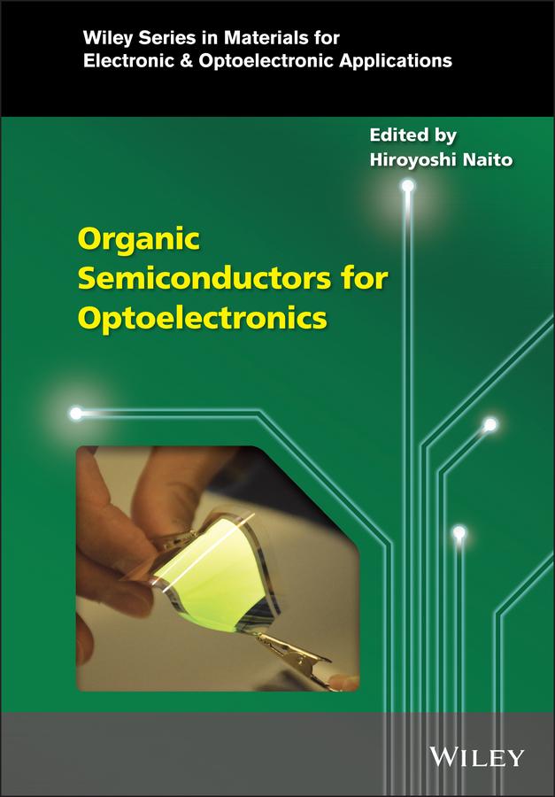
whichhasacontinuousparabolicshapewithavariable k asshowninFigure1.3.The plotoftheenergyvaluedependingon k isgenerallycalledenergybandorbandstructure.Accordingtothenumberofelectrons,thereappearstheupperlimitofenergy levelsfilledwithelectronscalledFermienergy(��F )dividingboththevalenceandconductionbands.Thewavevectoratthepositionof ��F iscalledFermiwavevector k F .Note that ±k givesthesameenergysignifyingthedegeneracyaccordingtoinversionofthe momentum,whichisalsomentionedastime-reversalsymmetryduetothechangeof momentumdirection.
Figure1.3 Energybandofafreeelectron. ��F and k F signifyFermienergyandFermiwavevector, respectively.
Figure1.4 Modelpotentialof1D crystal.
1.2.2Tight-BindingFramework
1.2.2.1Formalism
Thenextstepistointroduceaninfinitearrayoftheunitcellsintheconcerningorganic 1DcrystalstructurealreadyshowninFigure1.2.Thisconceptsimultaneouslybrings aboutthespatialregulararrayofpotentials V (x)inFigure1.4intotheSchrödinger equationas
with a beingthetranslationlength.Severalexamplesofunitcellsintheorganic1Dand 2DcrystalsaregiveninFigure1.5.
Inordertoobtaintheplausiblewavefunctionforgeneral1DcrystalwithinfiniterepetitionoftheunitcellsshowninFigure1.2,periodicboundarycondition(orBorn-von Karmanboundarycondition)isintroducedtowardsimplemathematicaltreatmentas intheordinarysolid-statephysics.Thisconditionisembodiedbyconsideringahuge “ring”withaninfinitediameterconsistingofaninfinitearrayoftheunitcellsasshown inFigure1.6.Thismakesthe1Dfree-electronwavefunctioninEq.(1.3)changeintothe 1DBlochfunctionwhichsatisfiestherelationship
�� (x + a)= exp[ika]�� (x)
where,again, k signifiesthewavevectorand a thetranslationlength.TheBlochfunction isconsideredasdeformationofthefree-electronwavefunctionintothatmodulatedby
Figure1.5 Examplesof1D(a),(b)and2D(c),(d)crystalsandtheunitcells(showninparentheses,oval, orsquare).Thearrowsindicatethedirection(s)ofthetranslation.
Each circle stands for the unit cell
Figure1.6 Periodicboundaryconditionexpressedbyaringwithaninfinitelylargediameter.Thefirst unitcell(blackcircle)becomesoverlappedwiththelastunitcellaftertheinfinitetranslation.
thearrayoftheunitcellscontainingtheatomsormolecules.AlsonotethatEq.(1.8) signifiesthatthetranslatedwavefunction �� (x + a)isrepresentedbymultiplicationof thephasefactorexp[ika]totheoriginalfunction �� (x).Thevalueof k rangesfrom–�� /a to �� /a,whichiscalledthefirstBrillouinzoneorsimplyBrillouinzone.
Quantumchemicaltreatmentoforganicmoleculesaregenerallybasedonthelinear combinationofatomicorbitals(LCAO)framework,whichcanalsobebroughtabout intotheBlochfunctionfororganiccrystal.[1]ThisiscalledCOaftertheconventional MOashasbeenalreadymentionedabove.TheCOisexpressedby
Table1.1 Typicalmethodsforcrystalorbital(CO)calculation
MethodofcalculationFeatures
Hückelforonly π electrons totalenergyunhandled spinsunhandled
ExtendedHückelforallthevalenceelectrons bandgapunreliable totalenergyunhandled spinsunhandled
VEH(Valence-effectiveHamiltonian)forallthevalenceelectrons seldomusedrecently employsadjustableparameters
SemiempiricalHartree-Fock (CNDO,INDO,MINDO,MNDO, AM1,etc.)
forallthevalenceelectrons seldomusedrecently employsadjustableparameters totalenergylessreliable bandgapoverestimated
Hartree-Fockforalltheelectrons totalenergyplausible structuraloptimizationpossible bandgapoverestimated
DFT(Densityfunctionaltheory)foralltheelectrons totalenergyplausible structuraloptimizationpossible bandgapplausible
where N formallystandsforthetotalnumberoftheunitcellnumberedby j, �� �� (x – ja) forthe �� -thatomicorbital(AO)involvedinthe j-thunitcell, s theenergylevelof �� s (k , x),and C �� ,s (k )thecoefficient.Amongthesevariables,thecoefficients C �� ,s (k )areinitially unknownandtheirvaluesaretobevariationallydeterminedbysolvingthecorrespondingSchrödingerequationintermsofthesecularequation.Notethat N isinfinitein actuality,sincethereareaninfinitenumberoftheunitcellsinFigure1.6.
Theconceptemployedaboveisoftenmentionedasthetight-bindingmethod,since thewavefunction,basedonthefree-electron,isnowmodulatedbyAOsneartheatomic regioninvolvedineachunitcell.Inthissense,theCOsstillremaincomplexfunctions. Itisstraightforwardtoshowthatthetight-bindingwavefunctioninEq.(1.9)satisfies therelationshipinthe1DBlochfunctionofEq.(1.8).Thereareseveralapproximation methodsfortheactualcalculationofCOs,whicharebasicallysimilartothoseforthe conventionalMOcalculations.TypicalcalculationmethodsarelistedinTable1.1.Afew softwarepackagesarecommerciallyavailablefortheCOcalculations.
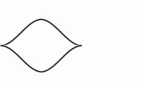
TheproceduretoobtaintheCOalsogivestheenergylevel ��s (k )ofeach �� s (k , x).Since ��s (k )isobtainedateach k continuouslyexistingintheBrillouinzoneintherange[–�� /a, �� /a]mentionedabove,itconstructsanenergy-bandstructureforeach s atthesame time,similartothatofafreeelectroninFigure1.3.Asimpleimageoftwoenergybands
Figure1.7 Schematicdrawingofthevalenceandtheconductionbands. obtainedbythetight-bindingschemeisillustratedinFigure1.7,wheretwoelectrons aresuppliedperunitcell.Notethattwoelectronsperunitcelloccupyonebandintotal. Inthiscase,theenergeticallylowerpartoftheenergybandisoccupiedbytheelectron andtheupperpartisunoccupied.Theoccupiedbranchiscalledthevalencebandand theunoccupiediscalledtheconductionband.
1.2.2.2SimpleExample
Inordertounderstandtheelectronicstructureoftheorganic1Dcrystal,itwillbeappropriatetostartfromanexplanationoftheband-structureanalysisofthesimplestinfinite 1Dchainwithiso-distantarrayoflattice;theunitcellofwhichconsistsofsingleatom A,thetranslationlengthbeing a asinFigure1.8a.ThisatomAcanalsobesubstituted byatomicgrouporso.Forinstance,whenAischangedintoaCHgroup,thischain canbeconsideredasnon-bondalternantpolyacetyleneinFigure1.8b.LetusexaminetheelectronicstructureofthissystemwithintheframeworkofthesimpleHückel approximation.Thesecularequationinthiscaseisexpressedby
where �� denotestheCoulombintegraloftheAOonA, �� theresonanceintegralbetween theadjacentAOs,and a thetranslationlengthasdenotedinFigure1.8b.Notethatboth �� and �� areofnegativevalues.Theresonanceintegral �� isalsocalledthetransferintegral t (t =−�� )insolid-statephysics.Thevariable k signifiesthewavevectorintheBrillouin zone[ �� /a, �� /a]andtheeigenvalue ��s isthefunctionof k . Thebandstructureofthe1Diso-distantchainisthenobtainedasshowninFigure1.9a fromtheeigenvalues ��1 (k )and ��2 (k )bysolvingEq.(1.10) ��1,2 (k )= �� ∓ √2�� 2 (1 + cos ka) (1.11)
Itisseenthatat k =± �� a ,thehighestoccupied(HO)band ��1 (k ),andthelowestunoccupied(LU)band ��2 (k )sticktogethertogivethezero-bandgap.Hence,the1Diso-distant chainshouldhavethemetallicproperty.
Conduction
Figure1.8 InfiniterepetitionofatomsAand(b)polyacetylenewiththeiso-distanttranslationlength. (c)and(d)representthebond-alternantcases.
Figure1.9 Bandstructurescorrespondingtothe1Dpolymersin(a)Figure1.8(a),(b),and(b) Figure1.8(c),(d).Notethatthetranslationlength a in(b)istwiceaslongasthatin(a)duetothe dimerizationinFigure1.8.
Next,letusconsiderthecaseinwhichtheabove1Dchainisnotiso-distantbutwith alternantdistance(say,1Dalternantchain)asinFigure1.8c.Inthiscase,twokindsof resonanceintegrals �� and �� ′ existcorrespondingto,e.g.,A=AandA-A,bonds,respectively(|�� | > |�� ′ |).Thischaincanalsobeconsideredsimilartothebond-alternantpolyacetyleneinFigure1.8d.Thesecularequationforthe1Dalternantchainisthengiven by
wherethecorrespondingeigenvaluesareobtainedas
Crystal orbital (CO)
Eigenvalues
Energy band
Shape and location
1.2ElectronicStructuresofOrganicCrystallineMaterials
As it is Squared (Product with its complex conjugate)
Expectaion value for the Hamiltonian
Inversed differential
Orbital patterns (Real function at k = 0, ��/a)
Electron density, Spin density
Total electronic energy (per unit cell)
Density of states (DOS)
Band gap (∆Eg), Electron affinity (Ea), Ionization potential (Ip), Band width (W ), Effective mass (m*)
Figure1.10 Electronicpropertiesderivedfromthecrystalorbital(CO).
Thebandstructureofthe1DalternantchainisillustratedinFigure1.9b,wherethe bandgap ΔE g appearswiththevalue
Thissignifiesthatthe1Dalternantchainshouldshowsemiconductiveorinsulating propertydependingonthevalueof ΔE g ,whichisalsotrueforthebond-alternantpolyacetylene.
Itisaninterestingproblemtopredictwhichsystemisthemoreenergeticallystable, the1Diso-distantorthe1Dalternantchainintheabove.Theanswertothisquestion willbediscussedinSection.1.4.1.
1.2.3ElectronicPropertiesBasedontheElectronicStructure
Severalpiecesofusefulinformationontheelectronicpropertiesoforganic1Dcrystal canbeobtainedfromtheBloch-typeCO �� s (k , x)anditsenergylevel ��s (k ),thediagram ofwhichisshowninFigure1.10.Inthefollowing,thesewillbedescribeditembyitem.
1.2.3.1CharacteristicsoftheEnergyBand
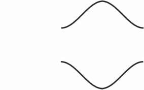
Theenergy-bandstructureoforganiccrystalsaffordsmuchinformationsuchasband gap,bandwidth,ionizationpotential,electronaffinity,andsoonasseeninwhatfollows. Inparticular,thehighestoccupied(HO)andthelowestunoccupied(LU)bandsoften playcrucialrolesnotonlyinelectronicpropertybutalsochemicalreactivity.Thoughit israthertiresometoexaminealltheenergybandsoftheorganic1Dcrystal,theanalysesoftheHOandtheLUbandsandtheirneighboringbandsoftengiveussufficient informationtoconsidertheessentialelectronicproperties. ItisofnotethattheclassificationofCOsbasedonthesymmetrysuchas, σ or π character,forexample,reflectsthecorrespondingenergyband.Thesymmetryforthe1D crystalstemsfromthelineargroupinthespacesymmetrybeingabitdifferentfrom thepointgrouptowhichtheordinarymoleculesbelong.Forinstance,theenergy-band structureofpolythiophenewithinfinitechainlength,asanexampleoforganic1Dcrystal,isshowninFigure1.11a.Here,crossingof σ and π bandsareseen.Thefactthat


Figure1.11 (a)BandstructureandDOSwiththeunitcellofpolythiopehene,(b)theHOCOpattern, and(c)theLUCOpattern.CalculationwasdonebyCrystal06softwarewithB3LYP/6-21G**.Boththe HOCOandLUCOat k = 0and �� /a areof �� -types(Topview).AlsonotethatthebothHOandtheLU bandsareof �� type.
Table1.2 Electronicpropertiesofpolythiophenea)
Quantity Value
Bandgap2.003eV
HObandwidth4.292eV
LUbandwidth3.829eV
Ionizationpotential4.496eV
Electronaffinity2.493eV
Effectivemass(TopoftheHOband)
0.520 m0
Effectivemass(BottomoftheLUband)0.560 m0
a)AlsoseethecaptionofFigure1.11.
thesecrossingscantakeplacecomesfromthesymmetryruleofthelineargroup,which hasbeendiscussedelsewhere.[2–4]NotethatinFigure1.11atheupperpartofthe HObandsandthewholeoftheLUbandsarebothof π-typeleadingtotheextended π-conjugationtowardthe1Ddirectionor,inotherwords,throughoutthepolymerchain, whichisappropriatetotheintrachainconductionpathsforbothholesandelectrons. Electronicpropertiesaccompaniedwiththebandstructureofpolythiophenearelisted inTable1.2.Thebandstructurecanbeexperimentallyobtainedbytheangleresolved photoelectronspectroscopy(ARPES)method.